ICGOO在线商城 > 分立半导体产品 > 晶体管 - FET,MOSFET - 阵列 > DMN6040SSD-13
 Datasheet下载
- 型号: DMN6040SSD-13
- 制造商: Diodes Inc.
- 库位|库存: xxxx|xxxx
- 要求:
| 数量阶梯 | 香港交货 | 国内含税 |
| +xxxx | $xxxx | ¥xxxx |
查看当月历史价格
查看今年历史价格
DMN6040SSD-13产品简介:
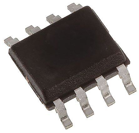
ICGOO电子元器件商城为您提供DMN6040SSD-13由Diodes Inc.设计生产,在icgoo商城现货销售,并且可以通过原厂、代理商等渠道进行代购。 DMN6040SSD-13价格参考。Diodes Inc.DMN6040SSD-13封装/规格:晶体管 - FET,MOSFET - 阵列, 2 个 N 沟道(双) Mosfet 阵列 60V 5A 1.3W 表面贴装 8-SO。您可以下载DMN6040SSD-13参考资料、Datasheet数据手册功能说明书,资料中有DMN6040SSD-13 详细功能的应用电路图电压和使用方法及教程。
Diodes Incorporated的DMN6040SSD-13是一款晶体管FET(场效应晶体管),具体为MOSFET(金属氧化物半导体场效应晶体管)阵列。该型号主要用于低电压、低电流的应用场景,具有高效能和小尺寸的特点。

 应用场景:

1. 便携式电子设备:
   DMN6040SSD-13适用于各种便携式电子设备,如智能手机、平板电脑、智能手表等。它能够有效管理电源管理和信号切换,确保设备在低功耗状态下运行,延长电池寿命。

2. 消费电子产品:
   在消费电子产品中,如蓝牙耳机、无线鼠标、键盘等,这款MOSFET阵列可以用于电源开关、负载开关和逻辑电平转换等应用,提供稳定可靠的性能。

3. 物联网(IoT)设备:
   对于物联网设备,如传感器节点、智能家居设备等,DMN6040SSD-13可以用于控制信号传输和电源管理,确保设备在低功耗模式下高效工作,同时支持快速响应和数据传输。

4. 可穿戴设备:
   在可穿戴设备中,如健身追踪器、健康监测设备等,该MOSFET阵列可以用于电源管理模块,确保设备在长时间使用过程中保持低功耗,同时提供稳定的电源输出。

5. 工业自动化:
   在工业自动化领域,如PLC(可编程逻辑控制器)、传感器接口等,DMN6040SSD-13可以用于信号隔离和电源切换,确保系统的可靠性和稳定性。

6. 汽车电子:
   在汽车电子系统中,如车载信息娱乐系统、车身控制系统等,该MOSFET阵列可以用于电源管理和信号切换,确保系统的高效运行和安全性。

 总结:
DMN6040SSD-13凭借其低导通电阻、小封装和高效能的特点,广泛应用于便携式电子设备、消费电子产品、物联网设备、可穿戴设备、工业自动化和汽车电子等领域。它能够在低电压、低电流的应用场景中提供卓越的性能和可靠性,满足现代电子设备对小型化、低功耗和高性能的需求。
| 参数 | 数值 |
| 产品目录 | |
| 描述 | MOSFET 2N-CH 60V 5A 8SOMOSFET MOSFET BVDSS: 41V-60 1V-60V SO-8 T&R 2.5K |
| 产品分类 | FET - 阵列分离式半导体 |
| FET功能 | 逻辑电平门 |
| FET类型 | 2 个 N 沟道(双) |
| Id-ContinuousDrainCurrent | 5 A |
| Id-连续漏极电流 | 5 A |
| 品牌 | Diodes Incorporated |
| 产品手册 | |
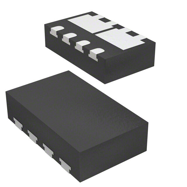
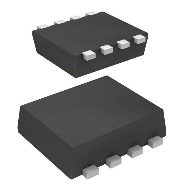
| 产品图片 |
|
| rohs | 符合RoHS无铅 / 符合限制有害物质指令(RoHS)规范要求 |
| 产品系列 | 晶体管,MOSFET,Diodes Incorporated DMN6040SSD-13- |
| 数据手册 | |
| 产品型号 | DMN6040SSD-13 |
| PCN设计/规格 | |
| Pd-PowerDissipation | 1.7 W |
| Pd-功率耗散 | 1.7 W |
| Qg-GateCharge | 22.4 nC |
| Qg-栅极电荷 | 22.4 nC |
| RdsOn-Drain-SourceResistance | 55 mOhms |
| RdsOn-漏源导通电阻 | 55 mOhms |
| RoHS指令信息 | http://diodes.com/download/4349 |
| Vds-Drain-SourceBreakdownVoltage | 60 V |
| Vds-漏源极击穿电压 | 60 V |
| Vgs-Gate-SourceBreakdownVoltage | +/- 20 V |
| Vgs-栅源极击穿电压 | 20 V |
| Vgsth-Gate-SourceThresholdVoltage | 3 V |
| Vgsth-栅源极阈值电压 | 3 V |
| 上升时间 | 8.1 ns |
| 下降时间 | 4 ns |
| 不同Id时的Vgs(th)(最大值) | 3V @ 250µA |
| 不同Vds时的输入电容(Ciss) | 1287pF @ 25V |
| 不同Vgs时的栅极电荷(Qg) | 22.4nC @ 10V |
| 不同 Id、Vgs时的 RdsOn(最大值) | 40 毫欧 @ 4.5A,10V |
| 产品种类 | MOSFET |
| 供应商器件封装 | 8-SO |
| 其它名称 | DMN6040SSD-13DICT |
| 典型关闭延迟时间 | 20.1 ns |
| 功率-最大值 | 1.3W |
| 包装 | 剪切带 (CT) |
| 商标 | Diodes Incorporated |
| 安装类型 | 表面贴装 |
| 安装风格 | SMD/SMT |
| 封装 | Reel |
| 封装/外壳 | 8-SOIC(0.154",3.90mm 宽) |
| 封装/箱体 | SOIC-8 |
| 晶体管极性 | N-Channel |
| 最大工作温度 | + 150 C |
| 最小工作温度 | - 55 C |
| 标准包装 | 1 |
| 正向跨导-最小值 | 4.5 S |
| 漏源极电压(Vdss) | 60V |
| 电流-连续漏极(Id)(25°C时) | 5A |
| 系列 | DMN6040 |
| 通道模式 | Enhancement |
| 配置 | Dual |


PDF Datasheet 数据手册内容提取
DMN6040SSD DUAL N-CHANNEL ENHANCEMENT MODE MOSFET Product Summary Features and Benefits ID Low Input Capacitance V(BR)DSS RDS(ON) Max Low On-Resistance N TA = +25°C Fast Switching Speed O 40mΩ @ VGS = 10V 5.0A Totally Lead-Free & Fully RoHS Compliant (Notes 1 & 2) I 60V AT 55mΩ @ VGS = 4.5V 4.4A Halogen and Antimony Free. “Green” Device (Note 3) Qualified to AEC-Q101 Standards for High Reliability M An Automotive-Compliant Part is Available Under Separate R Data Sheet (DMN6040SSDQ) O F N Description and Applications Mechanical Data I E This new generation MOSFET is designed to minimize the on-state Case: SO-8 C resistance (RDS(ON)) and yet maintain superior switching performance, Case Material: Molded Plastic, “Green” Molding Compound. N making it ideal for high efficiency power management applications. UL Flammability Classification Rating 94V-0 A Moisture Sensitivity: Level 1 per J-STD-020 V D DC-DC Converters Terminal Connections: See Diagram A Power Management Functions Terminals: Finish – Tin Finish Annealed over Copper Leadframe. Backlighting Solderable per MIL-STD-202, Method 208 Weight: 0.074 grams (Approximate) S1 D1 D1 D2 G1 D1 S2 D2 G1 G2 G2 D2 S1 S2 Top View Top View Pin Configuration Equivalent Circuit Ordering Information (Note 4) Part Number Case Packaging DMN6040SSD-13 SO-8 2,500/Tape & Reel Notes: 1. No purposely added lead. Fully EU Directive 2002/95/EC (RoHS) & 2011/65/EU (RoHS 2) compliant. 2. See http://www.diodes.com/quality/lead_free.html for more information about Diodes Incorporated’s definitions of Halogen- and Antimony-free, "Green" and Lead-free. 3. Halogen- and Antimony-free "Green” products are defined as those which contain <900ppm bromine, <900ppm chlorine (<1500ppm total Br + Cl) and <1000ppm antimony compounds. 4. For packaging details, go to our website at http://www.diodes.com/products/packages.html. Marking Information = Manufacturer’s Marking N6040SD = Product Type Marking Code YYWW = Date Code Marking YY or YY = Year (ex: 16= 2016) WW = Week (01 - 53) DMN6040SSD 1 of 7 November 2016 Document number: DS35673 Rev. 5 - 2 www.diodes.com © Diodes Incorporated
DMN6040SSD Maximum Ratings (@TA = +25°C unless otherwise specified) Characteristic Symbol Value Units N Drain-Source Voltage VDSS 60 V O Gate-Source Voltage VGSS ±20 V TI SStetaatdey TTAA == ++2750°°CC ID 54..10 A MA Continuous Drain Current (Note 6) VGS = 10V t<10s TTAA == ++2750°°CC ID 65..63 A R Maximum Body Diode Forward Current (Note 6) IS 2.5 A O Pulsed Drain Current (10µs pulse, duty cycle = 1%) IDM 30 A F Pulsed Body Diode Forward Current (10μs Pulse, Duty Cycle = 1%) ISM 30 A N Avalanche Current (Note 7) L = 0.1mH IAS 14.2 A I Avalanche Energy (Note 7) L = 0.1mH EAS 10 mJ E C N Thermal Characteristics (@TA = +25°C unless otherwise specified) A V Characteristic Symbol Value Units AD Total Power Dissipation (Note 5) TTAA == ++2750°°CC PD 10..38 W Steady State 102 Thermal Resistance, Junction to Ambient (Note 5) t<10s RθJA 61 °C/W Total Power Dissipation (Note 6) TTAA == ++2750°°CC PD 11..71 W Steady State 75 Thermal Resistance, Junction to Ambient (Note 6) t<10s RθJA 50 °C/W Thermal Resistance, Junction to Case (Note 6) RθJC 14.5 Operating and Storage Temperature Range TJ, TSTG -55 to +150 °C Electrical Characteristics (@TA = 25°C unless otherwise specified) Characteristic Symbol Min Typ Max Unit Test Condition OFF CHARACTERISTICS (Note 8) Drain-Source Breakdown Voltage BVDSS 60 V VGS = 0V, ID = 250µA Zero Gate Voltage Drain Current IDSS 100 nA VDS = 60V, VGS = 0V Gate-Source Leakage IGSS 100 nA VGS = ±20V, VDS = 0V ON CHARACTERISTICS (Note 8) Gate Threshold Voltage VGS(TH) 1 3 V VDS = VGS, ID = 250µA Static Drain-Source On-Resistance RDS(ON) 3305 4505 mΩ VVGGSS == 14.05VV,, IIDD = = 4 3..55AA Forward Transfer Admittance |YFS| 4.5 S VDS = 10V, ID = 4.3A Diode Forward Voltage VSD 0.7 1.2 V VGS = 0V, IS = 1A DYNAMIC CHARACTERISTICS (Note 9) Input Capacitance CISS 1,287 Output Capacitance COSS 57 pF Vf =D S1 .=0 M25HVz, VGS = 0V Reverse Transfer Capacitance CRSS 44 Gate Resistance RG 1.2 Ω VDS = 0V, VGS = 0V, f = 1.0MHz Total Gate Charge (VGS = 10V) QG 22.4 TGoattael- SGoauterc Ceh Cahrgaerg (eV GS = 4.5V) QQGGS 140..94 nC VDS = 30V, ID = 4.3A Gate-Drain Charge QGD 3.0 Turn-On Delay Time tD(ON) 6.6 Turn-On Rise Time tR 8.1 ns VGS = 10V, VDD = 30V, RG = 6Ω, Turn-Off Delay Time tD(OFF) 20.1 ID = 4.3A Turn-Off Fall Time tF 4.0 Body Diode Reverse Recovery Time tRR 18 ns IS = 4.3A, di/dt = 100A/μs Body Diode Reverse Recovery Charge QRR 11.9 nC IS = 4.3A, di/dt = 100A/µs Notes: 5. Device mounted on FR-4 PC board, with minimum recommended pad layout, single sided. 6. Device mounted on FR-4 substrate PC board, 2oz copper, with thermal bias to bottom layer 1-inch square copper plate. 7. IAS and EAS rating are based on low frequency and duty cycles to keep TJ = +25°C. 8. Short duration pulse test used to minimize self-heating effect. 9. Guaranteed by design. Not subject to product testing. DMN6040SSD 2 of 7 November 2016 Document number: DS35673 Rev. 5 - 2 www.diodes.com © Diodes Incorporated
DMN6040SSD 20 20 VDS = 5.0V 16 16 N A) A) O T ( T ( I N N T E 12 E 12 R R A R R U U M C C R AIN 8 AIN 8 O R R F , DD , DD TA = 150°C IN I 4 I 4 TA = 125°C TA = 85°C E TA = 25°C C N 0 0 TA = -55°C A 0 0.5 1.0 1.5 2.0 2.5 3.0 0 1 2 3 4 5 V VDS, DRAIN-SOURCE VOLTAGE (V) VGS, GATE-SOURCE VOLTAGE D Fig.1 Typical Output Characteristic Fig.2 Typical Transfer Characteristics A 0.10 0.10 ) ) E ( 0.09 E ( C C AN 0.08 AN 0.08 T T S S SI 0.07 SI E E R R N- 0.06 N- 0.06 O O CE 0.05 CE ID = 3.5A ID = 4.5A R R U 0.04 VGS = 4.5V U 0.04 O O S S N- 0.03 N- RAI VGS = 10V RAI D 0.02 D 0.02 , N) , N) O 0.01 O DS( DS( R 0 R 0 0 4 8 12 16 20 0 1 2 3 4 5 6 7 8 9 10 I , DRAIN-SOURCE CURRENT V , GATE-SOURCE VOLTAGE (V) D GS Fig. 3 Typical On-Resistance vs. Fig. 4 Typical On-Resistance vs. Drain Current and Gate Voltage Drain Current and Gate Voltage 0.10 2.4 ) 2.2 E ( 0.09 VGS = 4.5V ANC 0.08 TA = 150°C ED) 2.0 VIGDS = = 1 100AV ESIST 0.07 URCE MALIZ 11..68 CE ON-R 00..0056 TTAA = = 8 152°5C°C RAIN-SOCE (NOR 11..24 VGIDS == 54A.5V N-SOUR 00..0034 TA = 25°C , DDS(ON)ESISTAN 01..80 AI RR 0.6 DR 0.02 TA = -55°C ON- 0.4 , ON) 0.01 0.2 S( RD 0 0 0 4 8 12 16 20 50 -25 0 25 50 75 100 125 150 I , DRAIN CURRENT T , JUNCTION TEMPERATURE (C) D J Fig. 5 Typical On-Resistance vs. Fig. 6 On-Resistance Variation with Temperature Drain Current and Temperature DMN6040SSD 3 of 7 November 2016 Document number: DS35673 Rev. 5 - 2 www.diodes.com © Diodes Incorporated
DMN6040SSD 0.10 4.0 ) TANCE ( 0.08 GE (V) 3.5 ON ESIS OLTA 3.0 TI N-R 0.06 VGS = 4.5V D V 2.5 MA CE O ID = 500mA SHOL 2.0 ID = 1mA R E NFOR RAIN-SOU 0.04 IVDG =S 2=0 20.m5VA GATE THR 11..05 ID = 250µA CE I , DS(ON) 0.02 V, GS(th) 0.5 D N R 0 0 -50 -25 0 25 50 75 100 125 150 -50 -25 0 25 50 75 100 125 150 A V TJ, JUNCTION TEMPERATURE (C) TJ, JUNCTION TEMPERATURE (C) D Fig. 7 On-Resistance Variation with Temperature Fig. 8 Gate Threshold Variation vs. Ambient Temperature A 20 F) 16 p E ( V) C NT ( TAN Ciss E 12 TA = 25°C CI R A R P U A C C E N C 8 O OUR NCTI Coss S U I, S 4 , JT Crss C f = 1MHz 0 0 0.2 0.4 0.6 0.8 1.0 1.2 0 5 10 15 20 25 30 VSD, SOURCE-DRAIN VOLTAGE (V) VDS, DRAIN-SOURCE VOLTAGE (V) Fig.9 Diode Forward Voltage vs. Current Fig. 10 Typical Junction Capacitance 100 VDS = 30V V) ID = 4.3A E ( 10 G A A) OLT NT ( D V RE 1 DC L R HO CU PW = 10s ES N PW = 1s R AI 0.1 H R PW = 100ms T D ATE I, D TJ(max) = 150°C PW = 10ms G 0.01 TA = 25°C PW = 1ms V GS VSiGnSg =le 1 P0uVlse PW = 100µs DUT on 1 * MRP Board 0.001 0 5 10 15 20 25 0.1 1 10 100 Q , TOTAL GATE CHARGE (nC) g V , DRAIN-SOURCE VOLTAGE (V) Fig. 11 Gate Charge FiDgSure 12 SOA, Safe Operation Area DMN6040SSD 4 of 7 November 2016 Document number: DS35673 Rev. 5 - 2 www.diodes.com © Diodes Incorporated
DMN6040SSD 1 D = 0.9 D = 0.7 E C D = 0.5 N N TA D = 0.3 O S SI I T E R 0.1 A L D = 0.1 M A M R R D = 0.05 E O H T F T N N D = 0.02 E I SI 0.01 E N D = 0.01 C A Rthja(t)=r(t) * Rthja R VAN r(t), T D = 0.005 DutRy tChjyac=le1,0 D0C=/tW1 / t2 D Single Pulse A 0.001 0.00001 0.0001 0.001 0.01 0.1 1 10 100 1000 t1, PULSE DURATION TIMES (sec) Figure 13 Transient Thermal Resistance DMN6040SSD 5 of 7 November 2016 Document number: DS35673 Rev. 5 - 2 www.diodes.com © Diodes Incorporated
DMN6040SSD Package Outline Dimensions Please see http://www.diodes.com/package-outlines.html for the latest version. N O SO-8 I T A M R O F SO-8 N Dim Min Max Typ I E A 1.40 1.50 1.45 E A1 0.10 0.20 0.15 C 1 b 0.30 0.50 0.40 N c 0.15 0.25 0.20 A D 4.85 4.95 4.90 V E 5.90 6.10 6.00 D b E1 3.80 3.90 3.85 A E1 E0 3.85 3.95 3.90 9° (All sides) 7° h Q he --- ---- 10..2375 45 c L 0.62 0.82 0.72 ° Q 0.60 0.70 0.65 4°±3° A All Dimensions in mm Gauge Plane Seating Plane R 0.1 e A1 E0 L D Suggested Pad Layout Please see http://www.diodes.com/package-outlines.html for the latest version. SO-8 X1 Dimensions Value (in mm) C 1.27 Y1 X 0.802 X1 4.612 Y 1.505 Y1 6.50 Y C X DMN6040SSD 6 of 7 November 2016 Document number: DS35673 Rev. 5 - 2 www.diodes.com © Diodes Incorporated
DMN6040SSD IMPORTANT NOTICE DIODES INCORPORATED MAKES NO WARRANTY OF ANY KIND, EXPRESS OR IMPLIED, WITH REGARDS TO THIS DOCUMENT, INCLUDING, BUT NOT LIMITED TO, THE IMPLIED WARRANTIES OF MERCHANTABILITY AND FITNESS FOR A PARTICULAR PURPOSE N (AND THEIR EQUIVALENTS UNDER THE LAWS OF ANY JURISDICTION). O I Diodes Incorporated and its subsidiaries reserve the right to make modifications, enhancements, improvements, corrections or other changes T without further notice to this document and any product described herein. Diodes Incorporated does not assume any liability arising out of the A application or use of this document or any product described herein; neither does Diodes Incorporated convey any license under its patent or M trademark rights, nor the rights of others. Any Customer or user of this document or products described herein in such applications shall assume R all risks of such use and will agree to hold Diodes Incorporated and all the companies whose products are represented on Diodes Incorporated website, harmless against all damages. O F Diodes Incorporated does not warrant or accept any liability whatsoever in respect of any products purchased through unauthorized sales channel. N Should Customers purchase or use Diodes Incorporated products for any unintended or unauthorized application, Customers shall indemnify and I hold Diodes Incorporated and its representatives harmless against all claims, damages, expenses, and attorney fees arising out of, directly or E indirectly, any claim of personal injury or death associated with such unintended or unauthorized application. C N Products described herein may be covered by one or more United States, international or foreign patents pending. Product names and markings A noted herein may also be covered by one or more United States, international or foreign trademarks. V This document is written in English but may be translated into multiple languages for reference. Only the English version of this document is the D final and determinative format released by Diodes Incorporated. A LIFE SUPPORT Diodes Incorporated products are specifically not authorized for use as critical components in life support devices or systems without the express written approval of the Chief Executive Officer of Diodes Incorporated. As used herein: A. Life support devices or systems are devices or systems which: 1. are intended to implant into the body, or 2. support or sustain life and whose failure to perform when properly used in accordance with instructions for use provided in the labeling can be reasonably expected to result in significant injury to the user. B. A critical component is any component in a life support device or system whose failure to perform can be reasonably expected to cause the failure of the life support device or to affect its safety or effectiveness. Customers represent that they have all necessary expertise in the safety and regulatory ramifications of their life support devices or systems, and acknowledge and agree that they are solely responsible for all legal, regulatory and safety-related requirements concerning their products and any use of Diodes Incorporated products in such safety-critical, life support devices or systems, notwithstanding any devices- or systems-related information or support that may be provided by Diodes Incorporated. Further, Customers must fully indemnify Diodes Incorporated and its representatives against any damages arising out of the use of Diodes Incorporated products in such safety-critical, life support devices or systems. Copyright © 2016, Diodes Incorporated www.diodes.com DMN6040SSD 7 of 7 November 2016 Document number: DS35673 Rev. 5 - 2 www.diodes.com © Diodes Incorporated
Mouser Electronics Authorized Distributor Click to View Pricing, Inventory, Delivery & Lifecycle Information: D iodes Incorporated: DMN6040SSD-13