ICGOO在线商城 > 分立半导体产品 > 晶体管 - FET,MOSFET - 单 > DMG4466SSSL-13

 Datasheet下载
- 型号: DMG4466SSSL-13
- 制造商: Diodes Inc.
- 库位|库存: xxxx|xxxx
- 要求:
| 数量阶梯 | 香港交货 | 国内含税 |
| +xxxx | $xxxx | ¥xxxx |
查看当月历史价格
查看今年历史价格
DMG4466SSSL-13产品简介:
ICGOO电子元器件商城为您提供DMG4466SSSL-13由Diodes Inc.设计生产,在icgoo商城现货销售,并且可以通过原厂、代理商等渠道进行代购。 DMG4466SSSL-13价格参考¥1.76-¥1.76。Diodes Inc.DMG4466SSSL-13封装/规格:晶体管 - FET,MOSFET - 单, 表面贴装 N 沟道 30V 10A(Ta) 1.42W(Ta) 8-SO。您可以下载DMG4466SSSL-13参考资料、Datasheet数据手册功能说明书,资料中有DMG4466SSSL-13 详细功能的应用电路图电压和使用方法及教程。
| 参数 | 数值 |
| 产品目录 | |
| 描述 | MOSFET N-CH 30V 10A 8SO |
| 产品分类 | FET - 单 |
| FET功能 | 逻辑电平门 |
| FET类型 | MOSFET N 通道,金属氧化物 |
| 品牌 | Diodes Incorporated |
| 数据手册 | |
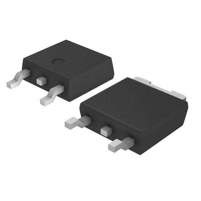
| 产品图片 |
|
| 产品型号 | DMG4466SSSL-13 |
| PCN其它 | |
| PCN设计/规格 | |
| rohs | 无铅 / 符合限制有害物质指令(RoHS)规范要求 |
| RoHS指令信息 | http://diodes.com/download/4349 |
| 产品系列 | - |
| 不同Id时的Vgs(th)(最大值) | 2.4V @ 250µA |
| 不同Vds时的输入电容(Ciss) | 478.9pF @ 15V |
| 不同Vgs时的栅极电荷(Qg) | 17nC @ 10V |
| 不同 Id、Vgs时的 RdsOn(最大值) | 23 毫欧 @ 10A,10V |
| 供应商器件封装 | 8-SO |
| 其它名称 | DMG4466SSSL-13DICT |
| 功率-最大值 | 1.42W |
| 包装 | 剪切带 (CT) |
| 安装类型 | 表面贴装 |
| 封装/外壳 | 8-SOIC(0.154",3.90mm 宽) |
| 标准包装 | 1 |
| 漏源极电压(Vdss) | 30V |
| 电流-连续漏极(Id)(25°C时) | 10A (Ta) |


- 商务部:美国ITC正式对集成电路等产品启动337调查
- 曝三星4nm工艺存在良率问题 高通将骁龙8 Gen1或转产台积电
- 太阳诱电将投资9.5亿元在常州建新厂生产MLCC 预计2023年完工
- 英特尔发布欧洲新工厂建设计划 深化IDM 2.0 战略
- 台积电先进制程称霸业界 有大客户加持明年业绩稳了
- 达到5530亿美元!SIA预计今年全球半导体销售额将创下新高
- 英特尔拟将自动驾驶子公司Mobileye上市 估值或超500亿美元
- 三星加码芯片和SET,合并消费电子和移动部门,撤换高东真等 CEO
- 三星电子宣布重大人事变动 还合并消费电子和移动部门
- 海关总署:前11个月进口集成电路产品价值2.52万亿元 增长14.8%


PDF Datasheet 数据手册内容提取
DMG4466SSSL N-CHANNEL ENHANCEMENT MODE MOSFET Product Summary Features and Benefits ID max Low On-Resistance V(BR)DSS RDS(ON) max TA = +25°C Low Input Capacitance 23mΩ @ VGS = 10V 10A Fast Switching Speed 30V 33mΩ @ VGS = 4.5V 8A Low Input/Output Leakage Low Gate Resistance Totally Lead-Free & Fully RoHS Compliant (Notes 1 & 2) Description Halogen and Antimony Free. “Green” Device (Note 3) This MOSFET has been designed to minimize the on-state resistance Qualified to AEC-Q101 Standards for High Reliability (RDS(ON)) and yet maintain superior switching performance, making it ideal for high efficiency power management applications. Mechanical Data Case: SO-8 Applications Case Material: Molded Plastic, "Green" Molding Compound. Backlighting UL Flammability Classification Rating 94V-0 Power Management Functions Moisture Sensitivity: Level 1 per J-STD-020 DC-DC Converters Terminal Connections Indicator: See diagram Terminals: Finish Matte Tin annealed over Copper leadframe. Solderable per MIL-STD-202, Method 208 e3 Weight: 0.074 grams (approximate) D S D SO-8 S D G S D G D S Top View Equivalent circuit Top View Internal Schematic Ordering Information (Note 4) Part Number Case Packaging DMG4466SSSL-13 SO-8 2500 / Tape & Reel Notes: 1. No purposely added lead. Fully EU Directive 2002/95/EC (RoHS) & 2011/65/EU (RoHS 2) compliant. 2. See http://www.diodes.com/quality/lead_free.html for more information about Diodes Incorporated’s definitions of Halogen- and Antimony-free, "Green" and Lead-free. 3. Halogen- and Antimony-free "Green” products are defined as those which contain <900ppm bromine, <900ppm chlorine (<1500ppm total Br + Cl) and <1000ppm antimony compounds. 4. For packaging details, go to our website at http://www.diodes.com/products/packages.html. Marking Information 8 5 8 5 = Manufacturer’s Marking G4466SS = Product Type Marking Code YYWW = Date Code Marking G4466SS G4466SS YY or YY = Year (ex: 13 = 2013) YY WW YY WW WW = Week (01 - 53) YY = Date Code Marking for SAT (Shanghai Assembly/ Test site) YY = Date Code Marking for CAT (Chengdu Assembly/ Test site) 1 4 1 4 Chengdu A/T Site Shanghai A/T Site DMG4466SSSL 1 of 6 September 2013 Document number: DS32244 Rev. 3 - 2 www.diodes.com © Diodes Incorporated
DMG4466SSSL Maximum Ratings (@TA = +25°C, unless otherwise specified.) Characteristic Symbol Value Unit Drain-Source Voltage VDSS 30 V Gate-Source Voltage VGSS ±20 V Continuous Drain Current (Note 5) SStetaatdey TTAA == ++2855°°CC ID 160 A Pulsed Drain Current (Note 5) IDM 60 A Avalanche Current (Notes 6) IAR 16 A Repetitive Avalanche Energy (Notes 6) L = 0.1mH EAR 12.8 mJ Thermal Characteristics Characteristic Symbol Value Unit Power Dissipation (Note 5) PD 1.42 W Thermal Resistance, Junction to Ambient @TA = 25°C (Note 5) RθJA 88.4 °C/W Operating and Storage Temperature Range TJ, TSTG -55 to +150 °C Electrical Characteristics (@TA = +25°C, unless otherwise specified.) Characteristic Symbol Min Typ Max Unit Test Condition OFF CHARACTERISTICS (Note 7) Drain-Source Breakdown Voltage BVDSS 30 — — V VGS = 0V, ID = 250μA Zero Gate Voltage Drain Current IDSS — — 1 μA VDS = 30V, VGS = 0V Gate-Source Leakage IGSS — — ±100 nA VGS = ±20V, VDS = 0V ON CHARACTERISTICS (Note 7) Gate Threshold Voltage VGS(th) 1.0 1.45 2.4 V VDS = VGS, ID = 250μA — 15 23 VGS = 10V, ID = 10A Static Drain-Source On-Resistance RDS (ON) 25 33 mΩ VGS = 4.5V, ID = 7.5A Forward Transfer Admittance |Yfs| — 2.5 — S VDS = 5V, ID = 10A Diode Forward Voltage VSD — 0.69 1 V VGS = 0V, IS = 1A DYNAMIC CHARACTERISTICS (Note 8) Input Capacitance Ciss — 478.9 — pF Output Capacitance Coss — 96.7 — pF Vf =D S1 .=0 M15HVz, VGS = 0V, Reverse Transfer Capacitance Crss — 61.4 — pF Gate Resistance Rg 0.4 1.1 1.6 Ω VDS = 0V, VGS = 0V, f = 1MHz Total Gate Charge (VGS = 4.5V) Qg — 5.0 8 nC Total Gate Charge (VGS = 10V) Qg — 10.5 17 Gate-Source Charge Qgs — 1.8 — nC VDS = 15V, VGS = 10V, ID = 10A Gate-Drain Charge Qgd — 1.6 — nC Turn-On Delay Time tD(on) — 2.9 — ns Turn-On Rise Time tr — 7.9 — ns VGS = 10V, VDS = 15V, Turn-Off Delay Time tD(off) — 14.6 — ns RG = 3Ω, RL = 1.5Ω Turn-Off Fall Time tf — 3.1 — ns Notes: 5. Device mounted on FR-4 substrate PC board, 2oz copper, with minimum recommended pad layout. 6. I and E rating are based on low frequency and duty cycles to keep T = 25°C AR AR J 7. Short duration pulse test used to minimize self-heating effect. 8. Guaranteed by design. Not subject to product testing. DMG4466SSSL 2 of 6 September 2013 Document number: DS32244 Rev. 3 - 2 www.diodes.com © Diodes Incorporated
DMG4466SSSL 30 20 VGS = 10V 25 VDS = 5V A) VGS = 4.5V A) 15 NT ( 20 VGS = 4.0V NT ( E E R R R R CU 15 VGS = 3.5V CU 10 AIN AIN VGS = 150°C DR 10 DR VGS = 125°C I, D I, D 5 VGS = 85°C 5 VGS = 3.0V VGS = 25°C VGS = 2.5V VGS = -55°C 0 0 0 0.5 1 1.5 2 2.5 3 3.5 4 4.5 5 0 0.5 1 1.5 2 2.5 3 3.5 4 V , DRAIN-SOURCE VOLTAGE (V) V , GATE-SOURCE VOLTAGE (V) DS GS Fig. 1 Typical Output Characteristic Fig. 2 Typical Transfer Characteristic ) 0.05 ) 0.04 E ( E ( VGS = 10V C C N N A 0.04 A ST ST 0.03 SI SI TA = 150°C E E N-R 0.03 VGS = 3.5V N-R TA = 125°C O O RCE VGS = 4.5V RCE 0.02 TA = 85°C OU 0.02 OU TA = 25°C S S RAIN- VGS = 10V RAIN- 0.01 TA = -55°C D 0.01 D , ON) , N) DS( S(O R 0 RD 0 0 5 10 15 20 25 30 0 5 10 15 20 25 30 I , DRAIN-SOURCE CURRENT (A) I , DRAIN CURRENT (A) D D Fig. 3 Typical On-Resistance Fig. 4 Typical On-Resistance vs. Drain Current and Gate Voltage vs. Drain Current and Temperature 1.7 0.06 ) E ( D) 1.5 VGIS == 54A.5V NC 0.05 E D A RCE MALIZ 1.3 VGS = 10V ESIST 0.04 UR I = 10A R OO D N- , DRAIN-SONSTANCE (N 01..91 SOURCE O 00..0023 VGIDS == 54A.5V SSI N- RDN-RE DRAI VIGDS = = 1 100AV O 0.7 , N 0.01 O S D R 0.5 0 -50 -25 0 25 50 75 100 125 150 -50 -25 0 25 50 75 100 125 150 TA, AMBIENT TEMPERATURE (°C) TA, AMBIENT TEMPERATURE (°C) Fig. 5 On-Resistance Variation with Temperature Fig. 6 On-Resistance Variation with Temperature DMG4466SSSL 3 of 6 September 2013 Document number: DS32244 Rev. 3 - 2 www.diodes.com © Diodes Incorporated
DMG4466SSSL 2.0 20 V) 18 E ( 1.8 G 16 A VOLT 1.6 NT (A) 14 OLD 1.4 ID = 1mA RRE 12 TA = 25°C H U S C 10 THRE 1.2 ID = 250µA RCE 8 E OU AT 1.0 S 6 , GH) I, S 4 S(T 0.8 G 2 V 0.6 0 -50 -25 0 25 50 75 100 125 150 0.2 0.4 0.6 0.8 1.0 1.2 T , AMBIENT TEMPERATURE (°C) V , SOURCE-DRAIN VOLTAGE (V) A SD Fig. 7 Gate Threshold Variation vs. Ambient Temperature Fig. 8 Diode Forward Voltage vs. Current 1,000 10,000 f = 1MHz Ciss A) F) NT (n1,000 TA = 150°C E (p RE NC UR TA = 125°C A C CIT 100 Coss GE 100 A A P K A Crss A C E C, , LS 10 TA = 85°C S D I TA = 25°C 10 1 0 5 10 15 20 25 30 0 5 10 15 20 25 30 V , DRAIN-SOURCE VOLTAGE (V) V , DRAIN-SOURCE VOLTAGE (V) DS DS Fig. 9 Typical Total Capacitance Fig. 10 Typical Leakage Current vs. Drain-Source Voltage 10 V) E ( 8 G A T L VO 6 VDS = 15V E ID = 10A C R U O S 4 E- T A G , GS 2 V 0 0 2 4 6 8 10 12 Q , TOTAL GATE CHARGE (nC) g Fig. 11 Gate-Charge Characteristics DMG4466SSSL 4 of 6 September 2013 Document number: DS32244 Rev. 3 - 2 www.diodes.com © Diodes Incorporated
DMG4466SSSL 1 CE D = 0.7 N D = 0.5 A T S D = 0.3 SI E R 0.1 AL D = 0.1 M ER D = 0.05 D = 0.9 H NT T D = 0.02 RRJAJ(tA) == 9r(0t)° C* /RWJA E NSI 0.01 D = 0.01 P(pk) A t1 R T D = 0.005 t2 r(t), DTJu t-y T CAy =c leP, *D R = JtA1(/tt2) D = Single Pulse 0.001 0.00001 0.0001 0.001 0.01 0.1 1 10 100 1,000 t , PULSE DURATION TIME (s) 1 Fig. 12 Transient Thermal Response Package Outline Dimensions Please see AP02002 at http://www.diodes.com/datasheets/ap02002.pdf for latest version. SO-8 Dim Min Max A - 1.75 4 5 A1 0.10 0.20 E1 E 0.2 Gauge Plane A2 1.30 1.50 A1 Seating Plane A3 0.15 0.25 L b 0.3 0.5 Detail ‘A’ D 4.85 4.95 E 5.90 6.10 E1 3.85 3.95 h 7°~9° 45° e 1.27 Typ h - 0.35 Detail ‘A’ A2 A A3 L 0.62 0.82 0 8 e b All Dimensions in mm D Suggested Pad Layout Please see AP02001 at http://www.diodes.com/datasheets/ap02001.pdf for latest version. X Dimensions Value (in mm) X 0.60 Y 1.55 C1 C1 5.4 C2 1.27 C2 Y DMG4466SSSL 5 of 6 September 2013 Document number: DS32244 Rev. 3 - 2 www.diodes.com © Diodes Incorporated
DMG4466SSSL IMPORTANT NOTICE DIODES INCORPORATED MAKES NO WARRANTY OF ANY KIND, EXPRESS OR IMPLIED, WITH REGARDS TO THIS DOCUMENT, INCLUDING, BUT NOT LIMITED TO, THE IMPLIED WARRANTIES OF MERCHANTABILITY AND FITNESS FOR A PARTICULAR PURPOSE (AND THEIR EQUIVALENTS UNDER THE LAWS OF ANY JURISDICTION). Diodes Incorporated and its subsidiaries reserve the right to make modifications, enhancements, improvements, corrections or other changes without further notice to this document and any product described herein. Diodes Incorporated does not assume any liability arising out of the application or use of this document or any product described herein; neither does Diodes Incorporated convey any license under its patent or trademark rights, nor the rights of others. Any Customer or user of this document or products described herein in such applications shall assume all risks of such use and will agree to hold Diodes Incorporated and all the companies whose products are represented on Diodes Incorporated website, harmless against all damages. Diodes Incorporated does not warrant or accept any liability whatsoever in respect of any products purchased through unauthorized sales channel. Should Customers purchase or use Diodes Incorporated products for any unintended or unauthorized application, Customers shall indemnify and hold Diodes Incorporated and its representatives harmless against all claims, damages, expenses, and attorney fees arising out of, directly or indirectly, any claim of personal injury or death associated with such unintended or unauthorized application. Products described herein may be covered by one or more United States, international or foreign patents pending. Product names and markings noted herein may also be covered by one or more United States, international or foreign trademarks. LIFE SUPPORT Diodes Incorporated products are specifically not authorized for use as critical components in life support devices or systems without the express written approval of the Chief Executive Officer of Diodes Incorporated. As used herein: A. Life support devices or systems are devices or systems which: 1. are intended to implant into the body, or 2. support or sustain life and whose failure to perform when properly used in accordance with instructions for use provided in the labeling can be reasonably expected to result in significant injury to the user. B. A critical component is any component in a life support device or system whose failure to perform can be reasonably expected to cause the failure of the life support device or to affect its safety or effectiveness. Customers represent that they have all necessary expertise in the safety and regulatory ramifications of their life support devices or systems, and acknowledge and agree that they are solely responsible for all legal, regulatory and safety-related requirements concerning their products and any use of Diodes Incorporated products in such safety-critical, life support devices or systems, notwithstanding any devices- or systems-related information or support that may be provided by Diodes Incorporated. Further, Customers must fully indemnify Diodes Incorporated and its representatives against any damages arising out of the use of Diodes Incorporated products in such safety-critical, life support devices or systems. Copyright © 2010, Diodes Incorporated www.diodes.com DMG4466SSSL 6 of 6 September 2013 Document number: DS32244 Rev. 3 - 2 www.diodes.com © Diodes Incorporated
Mouser Electronics Authorized Distributor Click to View Pricing, Inventory, Delivery & Lifecycle Information: D iodes Incorporated: DMG4466SSSL-13