
 Datasheet下载
- 型号: DLVR-L60D-E2NJ-C-NI5F
- 制造商: All Sensors
- 库位|库存: xxxx|xxxx
- 要求:
| 数量阶梯 | 香港交货 | 国内含税 |
| +xxxx | $xxxx | ¥xxxx |
查看当月历史价格
查看今年历史价格
DLVR-L60D-E2NJ-C-NI5F产品简介:
ICGOO电子元器件商城为您提供DLVR-L60D-E2NJ-C-NI5F由All Sensors设计生产,在icgoo商城现货销售,并且可以通过原厂、代理商等渠道进行代购。 DLVR-L60D-E2NJ-C-NI5F价格参考。All SensorsDLVR-L60D-E2NJ-C-NI5F封装/规格:压力传感器,变送器, 差分 压力 传感器 ±2.17 PSI(±14.95 kPa) 公型 - 0.08"(2.03mm) 双管 14 b 8-SMD 模块。您可以下载DLVR-L60D-E2NJ-C-NI5F参考资料、Datasheet数据手册功能说明书,资料中有DLVR-L60D-E2NJ-C-NI5F 详细功能的应用电路图电压和使用方法及教程。
| 参数 | 数值 |
| 产品目录 | |
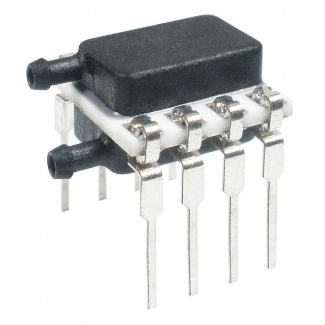
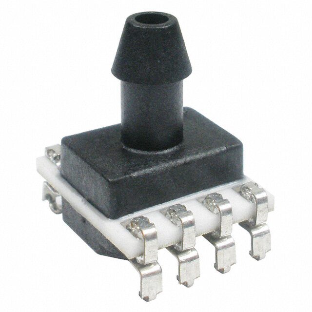
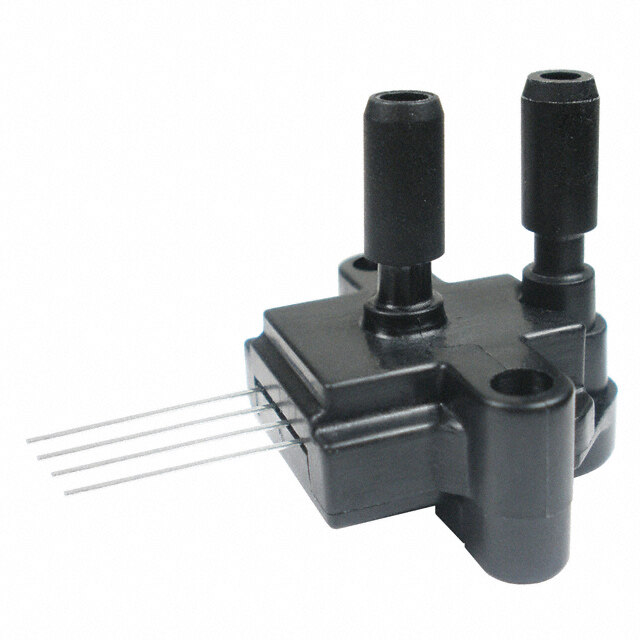
| 描述 | SENSOR PRESSURE 60" H2O 8SMD板机接口压力传感器 +/-60 inH2O Opp Side J-Lead SMT 5V |
| 产品分类 | |
| 品牌 | All Sensors Corporation |
| 产品手册 | |
| 产品图片 |
|
| rohs | 符合RoHS无铅 / 符合限制有害物质指令(RoHS)规范要求 |
| 产品系列 | 板机接口压力传感器,All Sensors DLVR-L60D-E2NJ-C-NI5FDLVR |
| mouser_ship_limit | 该产品可能需要其他文件才能进口到中国。 |
| 数据手册 | |
| 产品型号 | DLVR-L60D-E2NJ-C-NI5F |
| 产品种类 | 板机接口压力传感器 |
| 其它名称 | 442-1131 |
| 准确性 | 1 % |
| 出厂设置 | - |
| 压力类型 | - |
| 商标 | All Sensors |
| 安装风格 | SMD/SMT |
| 封装/外壳 | 8-SMD 模块 |
| 工作压力 | ±60" H2O |
| 工作温度 | -25°C ~ 85°C |
| 工作电源电压 | 5 V |
| 数字输出-位数 | 14 bit |
| 数字输出-总线接口 | I2C |
| 最大工作温度 | + 85 C |
| 最小工作温度 | - 25 C |
| 标准包装 | 1 |
| 特色产品 | http://www.digikey.cn/product-highlights/cn/zh/all-sensors-dlvr-series-low-volt-pressure-sensors/3956 |
| 电压-电源 | 5V |
| 电源电压-最大 | 6 V |
| 电源电流 | 5 mA |
| 端口大小 | 2.04 mm |
| 端口尺寸 | 公型,0.08"(2mm)双管 |
| 端口类型 | Dual Radial Barbless |
| 端子类型 | 表面安装 (SMD,SMT) |
| 精度 | 1% |
| 系列 | DLVR |
| 输出 | 数字 |
| 输出类型 | Digital |


- 商务部:美国ITC正式对集成电路等产品启动337调查
- 曝三星4nm工艺存在良率问题 高通将骁龙8 Gen1或转产台积电
- 太阳诱电将投资9.5亿元在常州建新厂生产MLCC 预计2023年完工
- 英特尔发布欧洲新工厂建设计划 深化IDM 2.0 战略
- 台积电先进制程称霸业界 有大客户加持明年业绩稳了
- 达到5530亿美元!SIA预计今年全球半导体销售额将创下新高
- 英特尔拟将自动驾驶子公司Mobileye上市 估值或超500亿美元
- 三星加码芯片和SET,合并消费电子和移动部门,撤换高东真等 CEO
- 三星电子宣布重大人事变动 还合并消费电子和移动部门
- 海关总署:前11个月进口集成电路产品价值2.52万亿元 增长14.8%

PDF Datasheet 数据手册内容提取
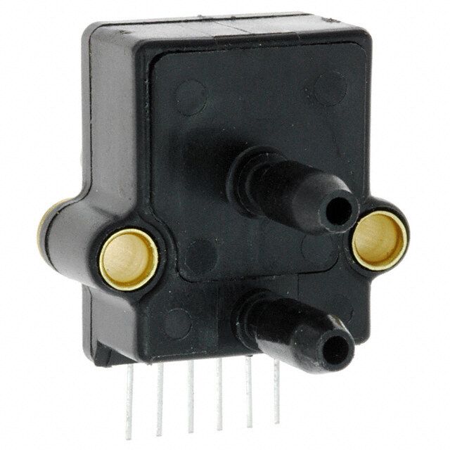
ile Swww F ig.al n nlse O ednso al DLVR Series Low Voltage Digital Pressure Sensors Ors.c o n rm gi Features ig R R i i mr • 0.5 to 60 inH2O Pressure Ranges n ors.cod O •• 3I2.3CV S Staunpdpalyrd V Ionltteargfea cSet a/n SdPaI rIdn t/e 5rfVa cOep Otipotnion al O ensne • Better than 1.0% Accuracy Over Temperature Typical n llsg Applications F a w.Si i w • Medical Breathing l w • Environmental Controls e • HVAC • Industrial Controls ile General Description • Portable/Hand-Held Equipment rs Swww F The DLVR Series Mini Digital Output Sensor is based on All Sensors’ CoBeam2 TM Technology. This reduces package stress o ig.al On scuosmceppatriebdil ittoy ,s rinesgulelt idnige dine ivmicperso.ved overall long term stability. The technology also vastly improves position sensitivity ens nedlsenso al The supply voltage options ease integration of the sensors into a wide range of process control and measurement sys- l s Ors.c n tems, allowing direct connection to serial communications channels. For battery-powered systems, the sensors can enter al rom gi very low-power modes between readings to minimize load on the power supply. ig R R i i mr These calibrated and compensated sensors provide accurate, stable output over a wide temperature range. This series m n ors.cod O icso ianttienngd ies do pfotiro unsael lwy iatvha niloabnl-ec oforrro msioveis,t nuoren/-hioanrsich wmoerdkiian gp rfloutiedcst isounc.h as air, dry gases and the like. A protective parylene sors.co al O nse en llsegn Standard Pressure Ranges Equivalent Circuit w.alls n F w.aSi ww i ww DDLeVvRic-eF 50D Op±er0a.5ti ningH R2aOn ge Pr1o0o0f PinreHs2sOur e Bu3r0s0t PinreHs2sOur e ±N6o,m55in3a clo Supnatns Vs 9 e le 7 DLVR-L01D ±1 inH2O 100 inH2O 300 inH2O ±6,553 counts 20 SCL 5 DLVR-L02D ±2 inH2O 100 inH2O 300 inH2O ±6,553 counts 22 n File DDDLLLVVVRRR---LLL012500DDD ±±±12500 i niinnHHH222OOO 222000000 iiinnnHHH222OOO 335000000 iiinnnHHH222OOO ±±±666,,,555555333 cccooouuunnntttsss I2C SIGNDnTAd 4314 f 408 Signwww.allse O DLVR-L30D ±30 inH2O 200 inH2O 500 inH2O ±6,553 counts 225 ednso nal DDLLVVRR--LL6001DG 0± t6o0 1 in inHH22OO 120000 iinnHH22OO 830000 iinnHH22OO ±136,,150573 ccoouunnttss Vs p 408 Orrs.com gi DLVR-L02G 0 to 2 inH2O 100 inH2O 300 inH2O 13,107 counts SPI SCLK ig R mR ri DLVR-L05G 0 to 5 inH2O 200 inH2O 300 inH2O 13,107 counts Option MISO 7 in ors.cod O DDLLVVRR--LL1200GG 00 ttoo 2100 iinnHH22OO 220000 iinnHH22OO 530000 iinnHH22OO 1133,,110077 ccoouunnttss SGSnd CA 9503 al O ensne DLVR-L30G 0 to 30 inH2O 200 inH2O 500 inH2O 13,107 counts Hill, n w.allsSig DLVR-L60G 0 to 60 inH2O 200 inH2O 800 inH2O 13,107 counts organ Fi w M l w Pressure Sensor Maximum Ratings Environmental Specifications vd. e Bl d Supply Voltage (Vs) 6 Vdc Temperature Ranges ar y Compensated: Commercial 0°C to 70°C e Common Mode Pressure 10 psig n File Lead Temperature (soldering 2-4 sec.) 270 °C OStpoe raragtein g Industrial -4-205°-C2°0C t° oCto 1to 82 8555 °°°CCC a 16035 Vi Sigwww.al n Humidity Limits (non condensing) 0 to 95% RH nlse O ednso al Ors.c o n All Sensors DS-0300 Rev D rm gi Page 1 ig R R i i mr n coO a ors.d l O nse en n llsg F a w.Si i w l w e
ile Swww F ig.al n nlse O ednso al Ors.c o n rm gi ig R Performance Characteristics for DLVR Series - Commercial and Industrial Temperature Range R i i ors.comd Or PAmaelAlr spauArrmeAmmeeenttetsre sA rrAer ew mitehA psuorseitdiV Aet p 3re.3ssVu r±e5 A%pp loierd 5 t.o0 Vp o±5r%t B (.depending onM selienct ed VoltAge oTptyiopn) excitAtion AnMd 2a5x°c unless otUhernwiistes s pecifieNd. oprteesssure nal O nse en Output Span 1 n llsg LxxD, FxxD - ±6,553 - Dec count F a w.Si LxxG - 13,107 - Dec count i w l w Offset Output @ Zero Diff. Pressure - e LxxD, FxxD - 8,192 - Dec count LxxG - 1,638 - Dec count Total Error Band 2 ile FL0510xD, L02x -- ±±00..6500 ±±11..50 %%SSppaann Swww F L05x, L10x, L20x, L30x, L60x - ±0.30 ±0.75 %Span ig.al n Span Temperature Shift 3 nlse O F50D, L01x, L02x - ±0.5 - %FSS ednso al O ff Ls0e5tx T, Le1m0xp, eLr2a0txu, rLe3 0Sxh, iLft6 0x - ±0 .2 - %F SS 3 Ors.c o n F50D, L01x, L02x - ±0.5 - %FSS rm gi L05x, L10x, L20x, L30x, L60x - ±0.2 - %FSS ig R mR ri Offset Warm-up Shift 4 in coO F50D, L01x, L02x - ±0.25 - %FSS a ors.d L05x, L10x, L20x, L30x, L60x - ±0.15 - %FSS l O nse Offset Position Sensitivity (±1g) - allsegn FL0550xD,, LL1001xx,, LL2002xx, L30x, L60x -- ±±00..1005 -- %%FFSSSS n F ww.Si Offset Long Term Drift (One Year) - il w F50D, L01x, L02x - ±0.25 - %FSS e L05x, L10x, L20x, L30x, L60x - ±0.15 - %FSS Linearity, Hysteresis Error 6 F50D - ±0.30 - %FSS ile LLxxxxDG -- ±±00..2150 -- %%FFSSSS Swww F Response Delay 5, 9 ig.al n Sleep - Wake Pressure - 0.40 0.50 ms nlse O Sleep - Wake All - 1.10 1.40 ms ednso al U p Pdoawteer -ROant eto First Reading Attempt 6.0 + 1 upd ate period - - m s 5 Ors.co n rm gi FNaosits e Reduced -- 01..4300 13..01 mmss ig R R i i mr Low Power - 6.5 9.5 ms n coO Digital Resolution - a ors.d Output Resolution - 14 - bit l O nse No Missing Codes 12 13 - bit en n llsg Temperature Output 7 F ww.aSi ROevseorlaullt iAocnc u racy -- 121 -- b°Cit il w Current Requirement (3.3V Option) 5 e Fast - 3.5 4.3 mA Noise Reduced - 3.6 4.5 mA Low Power - 0.72 0.90 mA ile C u Srlreeenpt (RIdeleq)u irement (5.0 Option) - 0. 5 5. 0 uA 5 Swww F Fast - 5.0 6.0 mA ig.al n Noise Reduced - 5.2 6.2 mA nlse O LSolewep P o(Iwdleer) -- 10..15 15..30 muAA ednso al See following page for performance characteristics table notes Ors.c o n DLVR Series Low Voltage Digital Pressure Sensors rm gi Page 2 ig R R i i mr n coO a ors.d l O nse en n llsg F a w.Si i w l w e
ile Swww F ig.al n nlse O ednso al Ors.c o n rm gi ig R I2C / SPI Electrical Parameters for DLVR Series R i i mr n coO Parameter Symbol Min Typ Max Units Notes a ors.d Input High Level - 80.0 - 100 % of Vs 5 l O nse en Input Low Level - 0 - 20.0 % of Vs 5 n allsg Output Low Level - - - 10.0 % of Vs 5 F w.Si i ww I2C Pull-up Resistor - 1000 - - Ω 5,8 le I2C Load Capacitance on SDA, @ 400 kHz CSDA - - 200 pF 5 I2C Input Capacitance (each pin) CI2C_IN - - 10.0 pF 5 ile rs Swww On F Snoptee c1:i fi tchaet isopnA nN iost tehse AlgeBrAic difference DBeLtVwRee nT rfaulnls sfceArl eF duenccimtiAol ncosu nts And the offset decimAl counts. enso igned.allsenso al NOTE 1: Pressure Output Transfer Function: l s Ors.c l o n a rm gi Where, 2 ig R R i Is the sensor 14 bit digital output. i mr Is the specified digital offset (gage = 1,638 and differential = 8,192) m n ors.cod O Ixs Ftuhlel Ssceanlseo Pr rFeuslslu Srcea)l e Span in inH2O (gage = Full Scale Pressure, differential = 2 sors.co al O nse en llsegn note 2: totAl e NrOrToEr 2 B: ATenmdp ecroatnusreis Otust opuft oTrfafnssefetr AFunndcti sopnA: n temperAture And cAliBrAtion errors, lineAritY And pressure hYsteresis errors, offset wArm-up shift, w.alls n F www.a Si nnnooottteee 345o::: f sspfAhhsriieffAttt m piissoe wtrseeiitrltiA hoistinn icV shteeh Atneors Af i2ticr5iVtsceit.tr YhiZ oAenudrd A olnofd ne nxgco titet Ar1tm0i0o o%nf tfAespsepttle idderd.i ftto e trhreo dres2V.i2c0e0. 79 e ww ile note 6: meAsur ed At one-hAlf full scAle rAted pressure using Best strAight line curVe fit. 20 5 note 7: temperA ture output conVersion function: 2 2 n File 𝑇𝑇𝑇𝑇𝑇𝑇𝑇𝑇𝑇𝑇𝑇𝑇𝑇𝑇𝑇𝑇𝑇𝑇𝑇𝑇𝑇𝑇 (℃)=𝑇𝑇𝑇𝑇𝑇𝑇𝑇𝑇𝑑𝑑𝑑𝑑𝑑𝑑×�21210−01�−50 4314 f 408 Signwww.allse O 225 ednso al nnoottee 89:: Afo plullolw-uinp gre sseinstsoorr ipso rweQeur-iruepd, t fhoer A cpoplrirceActtio i2nc m uussAtg we.A tiht eA tm lineAimsut mth VeA ilnudei cinAdteicdA ttiemde i Bs effoorr 5e. 0AVt toerm 3p.3tVin ogp teor Actoiomnm.unicAte with the sensor. p 408 Ors.co n rm gi ig R R i i mr 7 n coO 03 a ors.d CA 95 l O ensne Hill, n w.allsSig organ Fi w M l w d. e v Bl d ar y e n File a 16035 Vi Sigwww.al n nlse O ednso al Ors.c o n All Sensors DS-0300 Rev D rm gi Page 3 ig R R i i mr n coO a ors.d l O nse en n llsg F a w.Si i w l w e
ile Swww F ig.al n nlse O ednso al Ors.c o n rm gi ig R Device Options R i i mr n coO The following is a list of factory programmable options. Consult the factory to learn more about the options. a ors.d l O ensne Interface n llsg I2C and SPI interfaces are available. NOTE: SPI interface is only available with eight (8) lead packages. F a w.Si i ww Supply Voltage le Devices are characterized at either 3.3V or 5.0V depending on the options selected. It is suggested to select the option that most closely matches the application supply voltage for best possible performance. Speed/Power ile There are four options of Speed/Power. These are Fast(F), Noise Reduced(N), Low Power(L) and Sleep mode(S). Swww F ig.al n nlse O Fast Mode(F) Is the fastest operating mode where the device operates with continuous sampling at the ednso al fastest internal speed. Ors.c o n rm gi Noise Reduced(N): Also operates with continuous samples however the ADC is set for over sampling ig R R i for noise reduction. The conversion times are resultantly longer than the Fast(F) mode however, there is i mr n coO approximately 1/2 bit reduction in noise. a ors.d Low Power(L): Is similar to the Fast(F) mode with exception that the device uses an internal timer to l O nse delay between pressure conversions. The internal timer time-out triggers the next conversion cycle. The en n llsg update rate is commensurately lower for this mode as a result. F a w.Si i w Sleep(S): Is similar to the Low Power(L) mode however the trigger to initiate a sample comes from the l w user instead of an internal timer. This is ideal for very low update rate applications that requirelow e power usage. It is also ideal for synchronizing the data conversions with the host microprocessor. Coating ile Parylene Coating: Parylene coating provides a moisture barrier and protection form some harsh media. Con- Swww F sult factory for applicability of Parylene for the target application and sensor type. ig.al n nlse O ednso al Ors.c o n rm gi ig R R i i mr n coO a ors.d l O nse en n llsg F a w.Si i w l w e ile Swww F ig.al n nlse O ednso al Ors.c o n DLVR Series Low Voltage Digital Pressure Sensors rm gi Page 4 ig R R i i mr n coO a ors.d l O nse en n llsg F a w.Si i w l w e
ile Swww F ig.al n nlse O ednso al Ors.c o n rm gi ig R Operation Overview R i i mr n coO The DLVR is a digital sensor with a signal path that includes a sensing element, a 14 bit analog to digital converter, a DSP and a ors.d an IO block that supports either an I2C or SPI interface (see Figure 1 below). The sensor also includes an internal temperature l O nse reference and associated control logic to support the configured operating mode. The sensing element is powered down allsegn wADhCile t hnaott sbeeleincgts s tahme psilgedn atlo s coounrcsee rfvoer pthoew AeDr. CS.i nce there is a single ADC, there is also a multiplexer at the front end of the n F w.Si i w l w Figure 1 - DLVR Essential Model e al On File SensorVs ZTerooSPe/lTe/cZ210t SampleA DOSEanvmaebrp rrleaaleww PT/ CDonStProl PWTeraemkspeseurraeture I/O I2C/SPI l sensors Signed Owww.allsensors.c n Logic al rom gi ig R R i Gnd i mr m n ors.cod O sors.co al O nse en llsegn The ADC performs conversions on the raw sensor signal (P), the temperature reference (T) and a zero reference (Z) during an w.alls n F www.a Si AicsyD ccCalel lz.eedro a cNyocrlem. aItl aclyscol eh.a As caync olev ewrhsaemrep eliitnhge mr ao tdeem fopre raa ntuoriese m reedasuucreedm oeunttp ourt .z Ae rcooinngve isrs bioenin cgy cpleer tfohramt iesd m ise acsaullreidn ga pSrpeescsiuarle 9 e ww ile 7 0 The DSP receives the converted pressure and temperature information and applies a multi-order transfer function to com- 2 5 pensate the pressure output. This transfer function includes compensation for span, offset, temperature effects on span, tem- 2 2 On File pfTsLoyohernger gacricethau graaorleresne o dei zt effdwaveetoiictco eteensrsff m o oeanifcnn ttdoehiv ffsefe rst o iehonntept tea e Dtnrronead altb asilna yefc gucbkon me nlctitnowdieod eoaneerrssdni toae yAcrf cDcttohoeCmmre ds sppaienmeengnrpsa stotlhaeurte sri1, oe f)ta n heFc ffreftoeo ererrce ydtRgs ipuuff onrleaonnrrg eiibtnrnyoagt mtoi ahaflm n stddhpee ead2v n S)iP c Tpaoerneswigcd. eig aorel/ff rScespyedcet.l e.eT Tdshh eaoen pcrdeoti noiwstn hra o(elsslt oelhoe elgi Tnri aceob arp lrneeit or1yfto) c.t rTohmhmese Ap tCDheoneCn s patrteoiorl- n 225 4314 f 408 Signedwww.allsenso al forms the Over Sampling. Refer to Figure 2 for the communication model associated with the operating modes listed below. p 408 Ors.co n rm gi Fthrereee R oupntnioinngs Mavoadilea:b Ilne tthhea tf roepee rruanten iinng t hmeo Fdreee, c Rounnvneirnsgio mn coydcele (sF ,a Nre a inndit iLa)t. eTdw ion toefr tnhaellsye a (tF raengdu lNar) rinutne rcvoanlsti.n Tuhoeures layr we hile ig R R i i mr the third option (L) has an approximate 6 ms delay between conversion cycles. All three options have Special cycles 7 n coO inserted at regular intervals to accomplish the ADC zeroing and temperature measurements. Two of the options utilize 03 a ors.d oversampling. Refer to Table 1 for specific option controls. CA 95 l O ensne Triggered Mode: In the Triggered Mode, a conversion cycle is initiated by the user (or host uP). There are two available Hill, n w.allsSig mmeetahsuordesm toe nwta ckyec ltehse ( Zse, nT saonrd fr Po)m. T hsliese ppr omvoiddees. cTohme fiprlestt emlye ftrheosdh (dWataak fer oAmll) tish eto s ewnaskoer .t Thhee s seencsoonr da nmde ptherofdo r(mW aaklle t hPr)e ise organ Fi ww to wake the sensor from sleep and only perform the pressure measurement (P).When using this second method, it is up d. M le to the user to interleave Wake All commands at regular intervals to ensure there is sufficiently up to date temperature v Bl information. Also, the Wake Pressure method is only available from the I2C interface (not available using a SPI interface). d ar y e n File a 16035 Vi Sigwww.al n nlse O ednso al Ors.c o n All Sensors DS-0300 Rev D rm gi Page 5 ig R R i i mr n coO a ors.d l O nse en n llsg F a w.Si i w l w e
ile Swww F ig.al n nlse O ednso al Ors.c o n rm gi ig R Operation Overview (Cont’d) R i i mr n coO a ors.d Table 1 - DLVR Control Logic Detail l O ensne Control Logic n llsg Power/ Delay Normal Special Special F w.aSi Speed Power/Speed Operating Over Between ADC ADC ADC Cycle i w Description Mode Sample l w Option Samples Cycles Cycles Interval e F Fast No No 1 (P) 1 (Z or T) 255 Free N Noise Reduced Yes No 1 (P) 1 (Z or T) 255 Running L Low Power Yes Yes 1 (P) 1 (Z or T) 31 File S SSlleeeepp( 1()W (Wakaek eA lPl)ressure) Triggered NNoo UUsseerr DDeeffiinneedd 11 ((PP)) 2 (Zn /+a T) ANlweaveyrs Sigwww.al n Note 1) Wake from sleep with pressure only reading is not available with SPI interface (I2C only). nlse O ednso al Ors.c n Figure 2 - DLVR Communication Model rom gi ig R Free Running Mode [(F)ast, (N)oise Reduced and (L)ow Power Option] R i i mr Cycle Type Normal Cycle Normal Cycle Special Cycle (1) n ors.cod O NeInwte Drnaatla O Apvearialatbiolen DSP Delay ADC (P) DSP Delay ADC (P) DSP Delay ADC (P) ADC (T or Z) DSP Delay ADC (P) al O nse Note 1: See Table 1 for frequency of Special Cycles en n llsg F a w.Si i w Triggered Mode - Wake All [(S)leep Option] l w I2C Wake All Read Data Wake All e or SPI (SS) Read Data Internal Operation Sleep ADC (Z) ADC (T) ADC (P) DSP Sleep ADC (Z) ADC (T) ADC (P) DSP Sleep ile New Data Available Swww F ig.al n Triggered Mode - Wake Pressure [(S)leep Option] nlse O I2C Wake P. Read Data Wake P. ednso al Internal Operation Sleep ADC (P) DSP Sleep ADC (P) DSP Sleep Ors.c New Data Available o n rm gi ig R R i i mr n coO a ors.d l O nse en n llsg F a w.Si i w l w e ile Swww F ig.al n nlse O ednso al Ors.c o n DLVR Series Low Voltage Digital Pressure Sensors rm gi Page 6 ig R R i i mr n coO a ors.d l O nse en n llsg F a w.Si i w l w e
ile Swww F ig.al n nlse O ednso al Ors.c o n rm gi ig R mR ri Digital Interface Data Format in coO a ors.d For either type of digital interface, the format of data returned from the sensor is the same. The first 16 bits consist of l O nse the 2 Status bits followed by the 14-bit the pressure value. The third byte provides the 8 most significant bits of the mea- en n llsg sured temperature; the fourth byte provides the 3 least significant bits of temperature, followed by 5 bits of undefined F ww.aSi fisellnesr odra, toar. fWoliltohw eiinthge trh ien ttehrirfdac bey, tteh e(i fh jousstt mthaey m teorsmt-isnigatnei fithcaen ttr a8n bsiftesr oaff tteerm repceeriavtiunrge tahree finreset dtwedo) .b Ryetefesr o tof d Taatbal efr 2o mfo rt hthee il w overall data format of the sensor. Table 3 shows the Status Bit definition. e Table 2 - Output Data Format ile rs Swww F o ig.al al On BStita tDuesfi (nS)it: iNonosrm: al/command / busy / diagnostic l sens ned Olsensors.c n Pressure (P): Digital pressure reading al rom gi Temperature (T): Compensated temperature reading ig R R i i mr m n ors.cod O Table 3- Status Bit Definitions sors.co al O nse en llsegn w.alls n F w.aSi ww i ww I2C Interface 9 e le 7 0 2 I2C Communications Overview 25 2 n File Tsehqeu I2eCnc iBenusts ea rnnfaodct t eBh uuessirey a s( sIa)s: osDecutia rotinef gdsi gimdnlnaeel pmseeorqinouidecnss .cb Reoest fhfeo rdr t acoto aFm ilgimnuerue (n S3iDc faAot)rio atnhn.ed T achsloeso cfckoi lalliotnewed i( nSugCs aLisg) aere domef asthcinrei p HfotIiGloloHnw. oifn tgh sei gsunpalp soerqteude nces. 4314 f 408 Signwww.allse O START condition (ST): A HIGH to LOW transition of SDA line while the clock (SCL) is HIGH is interpreted as 225 ednso al SbTeAgRinT wcoitnhd ait SioTnA.R STT AcoRnTd ciotinodni.tions are always set by the master. Each initial request for a pressure value has to p 408 Ors.co n rm gi Slave address (An): The I²C-bus requires a unique address for each device. The DLVR sensor has a preconfig- ig R R i ured slave address (0x28). After setting a START condition the master sends the address byte containing the i mr 7 n coO 7 bit sensor address followed by a data direction bit (R/W). A "0" indicates a transmission from master to slave 03 a ensors.ned (AdWeckvRniIcToeEw, )w,l eahd "eg1t"eh ie(nArd moicraa Nstte)e:s r Da oa drt aaslt aiasv rteer,aq insu srefeesqtr ru(eRirdEe AidnD tu)o.n pitusl lo tfh 8e b ditast a(1 l ibnyet LeO) aWt ato t iamcek,n MowSBle fidrgset. r Eeaccehip dt aotfa t-hreec deaivtian. gT he Hill, CA 95 l On w.allsSig MNAaCstKe rc omnudsitt igoenn eexriasttes , aann dex ttrhae c slloacvke ptrualnses mfoirt ttehri sb pecuorpmoesse .i nIfa tchteiv ree. cTehiev emr adsoteesr ndoette prumlli nthees wdahteat hlinere tdoo swennd, a organ Fi w M l w the last command again or to set the STOP condition, ending the transfer. d. e v DATA valid (Dn): State of data line represents valid data when, after a START condition, data line is stable for Bl d duration of HIGH period of clock signal. Data on line must be changed during LOW period of clock signal. ar y There is one clock pulse per data bit. ne File DueAsT.A T hoep etrraantisomni:s Tshioen s emnasyo rb set ahratlst etod sbeyn tdh e4 hdoastat abfyteter sa cnoyn otfa tinhien gb ytthees cbuyr rreenspt opnredsisnugr ew aitnhd a t NemACpKe.r a ture val- a 16035 Vi Sigwww.al n STOP condition (P): LOW to HIGH transition of the SDA line while clock (SCL) is HIGH indicates a STOP condi- nlse O tion. STOP conditions are always generated by the master. ednso al Ors.c o n All Sensors DS-0300 Rev D rm gi Page 7 ig R R i i mr n coO a ors.d l O nse en n llsg F a w.Si i w l w e
ile Swww F ig.al n nlse O ednso al Ors.c o n rm gi ig R R i i mr I2C Communications Overview (Cont’d) n coO a ors.d l O nse en Figure 3 - I2C Communication Diagram n llsg F a w.Si I2C Communications Diagram i w l w 1. Start All ( to wake sensor from Sleep mode, Zero ADC, read Temperature and read Pressure ) e Set by bus master: -I - - S- T A6A5A4A3A2A1A0 R SP I Set by sensor: - - - - - - - - - - - - - - - - - - - - - - - - - - - - - A- - - - - - - - - ile 2. Start Pressure ( to wake sensor from Sleep mode and read Pressure only ) Swww n F SSeett bbyy bseuns smora:s -t e- r-: -- I -- -- S-- T- - A- 6- -A -5 - A- 4- -A -3 - A- 2- -A -1 -A -0 - -W - - A- - S- P- - I- - - - ign.allse O 3. Read Data ( with examples of reading pressure, pressure plus 8 bits of temperature and pressure plus 11 bits of temperature ) ednso al Set by bus master: -I - - S- T A6A5A4A3A2A1A0 R A Ors.c o n Set by sensor ( pressure plus status ): - - - - - - - - - - - -A - -D -3 1- -… - -D -24 D23… D16 rm gi …then, one of the following: ig R a) Set by bus master, to stop transfer after pressure data received: - - - - - - - - - - - - - -N - - -S -P - - I- - - - R i i mr --OR-- n coO b) Set by bus master, to stop transfer after first temperature data byte received: - - - - -A - - - - - - - - - N SP I a ors.d Set- b-Oy Rse--nsor ( high order 8 bits of temperature ): - - - - - - - - - - - - - - - - - - - - - - - - - - - D- 1-5 - -… - - -D -8 l O ensne c) Set by bus master, to stop transfer after last temperature data byte received: - - - - - A- - - - - - - - - A N SP I n llsg Set by sensor ( all 11 bits of temperature plus padding bits ): - - - - - - - - - - - - - - - - - - - D- 1- 5- - …- - -D -8 D7 … D0 F a w.Si i ww BIdules: states I SAe6n…sorA A0ddress DStaattau sfo:rmat D31D30 le Start: ST Default: 0x28 Pressure data: D29 … D16 Stop: SP Temperature data: D15 … D5 Ack: A (padding bits:) D4 … D0 ile N““RWaecraikted:”” bbiitt ((01)):: WNR Swww F ig.al n nlse O ednso al Figure 3 illustrates the sequence of signals set by both the host and the sensor for each command. Note that for the Da- Ors.co n taRead command, the host has the option of responding to the second or third bytes of data with a NACK instead of ACK. rm gi This terminates the data transmission after the pressure data, or after the pressure data and upper byte of temperature, ig R R i i mr have been transmitted. See Figure 6 for the I2C timing details. n coO a ors.d l O nse en n llsg F a w.Si i w l w e ile Swww F ig.al n nlse O ednso al Ors.c o n DLVR Series Low Voltage Digital Pressure Sensors rm gi Page 8 ig R R i i mr n coO a ors.d l O nse en n llsg F a w.Si i w l w e
ile Swww F ig.al n nlse O ednso al Ors.c o n rm gi ig R R i i mr I2C Command Sequence n coO a ors.d Depending on whether the Fast, Noise Reduced, Low-Power, or Sleep options have been selected, the command se- l O nse en quence differs slightly. See Figure 3 for details of the three I2C commands. n llsg F a w.Si i w l w Fast, Noise Reduced or Low-power Configuration e The part enters Free Running mode (see table 1) after power-up: it performs an initial complete measurement, writes the calculated data to the output registers, sets the INT pin high, then goes to sleep. After a delay deter- File mtphinien nies dg ig obn ybo atrhceked t,u otph sdelea heteop s.r taD ptaert ooacRpeetsiaosdon r,i stc htahene pr eoapnrtel ywa tci lotlh mwisma ckaoenm udpm r,e apcneodrgf uonnrimzteil d mt;h eaeas Sswutairtethum sth ebenit tSss l,ie nuedppidc caaottene fitahgneu u roaputditoapntue,t di fr ertehgaeisd tIiNenrTgs ,. ors Sigwww.al On Sleep Configuration ens nedlsenso al The part enters Triggered mode (see table 1) after power-up, and waits for a command from the bus master. If l s Ors.c l o n the StartAll command is received, the temperature, ADC zero, and pressure readings are all measured, and cor- a rm gi rection calculations are performed. When valid data is written to the output registers, the INT pin is set high, ig R mR ri and the processing core goes back to sleep. The host processor then sends the DataRead command to shift m in nsors.coed O otThhueet Dtrheaestp auoRpnedasaedt etcidom mvea mdlueaepnsed. n Iufd ntsht oiel n tIh NceoT nSptfiiangt uuisrs a nbtoiiotts nm i noodpnitciitoaotnrees td(hr,e atfhte etrh theoo vTsaat lbcualeens 1 ph aoanvllde t hbPeee re ofnou rutmppuadnta crteeegd Ci s(hstaeereras Tc batyeb rlrieesstp i2ces aa)t.nindg 3 ). ensors.co al O llsegn Depending on the application, pressure measurements may be performed by sending the StartPressure com- w.alls n F w.aSi mand, which only measures the pressure value and uses previously measured temperature data in calculating ww i ww tchoem cmomanpde. n Tshaitse cda onu btpe uat u vsaelufuel. m Thetish porde tsoe nstysn tchher orensizuelt t fhaes tseern (sino ra wboituht t1h/e3 hthoest d ceolnaytr toimlleer )a tsh wane ltlh aes SattatartinA-ll 9 e le ing the fastest overall response time without Special cycles occuring at unwanted times. The system designer 07 2 should determine the interval required for sending StartAll commands, necessary to refresh the internal 5 2 On File I2C Except1met. imu oSnepnincesadratiintougnr e ae vrSratoalurr tefo caro ntnhdde zi tenioreonx tp, tcohoienmnt m daa uStntao,i cpina ct oioornndd,e iert vitooenn m, iwfa tiinthhteao niunet xaatcn csyut atrrraatt nec osointuidotpintuiso ton vn ai stl uhceoes rC.reLcKt lainned, cthreea ctleosc ak cpoumls-e is 225 4314 f 408 2 Signedwww.allsenso al applied. A second Start condition must be set, which clears the error and allows communication to proceed. p 408 Ors.co n rm gi 2. The Restart condition—a falling SDA edge during data transmission when the CLK clock line is still high— ig R creates the same stall/deadlock. In the following data request, an additional Start condition must be sent for R i i mr correct communication. 7 n coO 03 a ors.d 3. A falling SDA edge is not allowed between the start condition and the first rising SCL edge. If using an I2C CA 95 l O ensne address with the first bit 0, SDA must be held low from the start condition through the first bit. Hill, n w.allsSig organ Fi w M l w d. e v Bl d ar y e n File a 16035 Vi Sigwww.al n nlse O ednso al Ors.c o n All Sensors DS-0300 Rev D rm gi Page 9 ig R R i i mr n coO a ors.d l O nse en n llsg F a w.Si i w l w e
ile Swww F ig.al n nlse O ednso al Ors.c o n rm gi ig R R i SPI Interface i mr n coO a ors.d SPI Command Sequence l O nse en DLVR sensors using the SPI interface option provide 3 signals for communication: SCLK, SS (Slave Select), and MISO. n llsg This read-only signaling uses a hardware protocol to control the sensor, differing slightly with the speed/power option F a w.Si selected as described below: i w l w Fast(F), Noise Reduced(N) and Low-Power(L) Configurations: After power-up, the part enters Free Running e mode and begins its periodic conversion cycle, at the interval determined by the programmed Power/Speed option. This is the simplest configuration. The only bus interaction with the host is the SPI DataRead opera- tions. Polling the sensor at a rate slower than the internal update rate will minimize bus activity and ensure ile tuhpadta nteewd dvaatlua easn adr eth per easbesnetnecde wofit ehr eroarc cho tnradnitsifoenr.s N. ote that the Status bits should still be checked to verify Swww F ig.al n Sleep(S) Configuration: As with the I2C option, the part enters Triggered mode after power-up, and waits for nlse O alo cwo mbym thane dh ofrsotm fo trh aet bleuass tm 8aussteecr., tThoe wn adkreiv tehne h pigarht. a Tnhdis s ctaarnt ba em deoanseu rbeym sehniftt icnygc lae ,d tuhme SmSy p biny tme uosf t8 b bei tds rfirvoemn ednso al the sensor. This bus activity can be considered the SPI StartAll command, where the rising edge of SS is the Ors.c n required input to start conversion. Updated conversion data is written to the output registers after a period rom gi dependent on configuration options ( see Performance Characteristics). After this update of the registers, the ig R R i core goes to an inactive (sleep) state. The DataRead command simply consists of shifting out 2, 3, or 4 bytes i ors.comd Or opwfra odkvaeitd taeh fdero. p mTahr teth wpeha sreetnn r estohmre.a Tninhesex ithn coaoscntt ivcveaern sf oicolhlnoe wicsk itn tohg be te hS iptsa ertreufaosd rbm oitpes deor.fa tthioen o, uatnpdu at ntoo tvheerrif Syt tahratAt lnl eowpe draattaio hna iss bneeeend ed to nal O nse llsegn SPI Bit Pattern n F a w.Si i w The sequence of bits and bus signals are shown in the following illustration (Figure 4). Refer to Figure 5 in the Interface l w Timing Diagram section for detailed timing data. As previously described, the incoming data may be terminated by rais- e ing SS after 2, 3, or 4 bytes have been received as illustrated below. Figure 4 - SPI Bit Pattern ile Swww F ig.al n nlse O ednso al Ors.c o n rm gi ig R R i i mr n coO a ors.d l O nse en n llsg F a w.Si i w l w e ile Swww F ig.al n nlse O ednso al Ors.c o n DLVR Series Low Voltage Digital Pressure Sensors rm gi Page 10 ig R R i i mr n coO a ors.d l O nse en n llsg F a w.Si i w l w e
ile Swww F ig.al n nlse O ednso al Ors.c o n rm gi Interface Timing Diagrams ig R R i i mr n coO a ors.d l O nse Figure 5 - SPI Timing Diagram en n llsg F a w.Si i ww tSCLK le tSSCLK tLOW tHIGH SCLK File MISO (HI•Z) (HI•Z) ors Sigwww.al On tCLKD tCLKD ens nedlsenso al SS l s Ors.c l o n a rm gi tCLKSS t ig R R i IDLE i mr m n ors.cod O SSPCCALLRKKA ccMllooETccEkkR ff rreeqquueennccyy ((41MMHHzz cclloocckk)) SYMffSSBCCOLL KKL M55IN00 TYP M82A00X00 UkkNHHITzzS sors.co al O w.allsensSigne MMCSlSiionn cdiimmkr ouuepmmd tg oSSe CC fitrLLosKK t d cccallloootaccckk kt r lheaoidnwgsgh wie twii odidntht h tttStCHSLLCOIGKLWDHK 2000...566 0.1 uuuussss www.allsen n Fi ww RBiusse foref eS Sti mreela btievetw teoe lans rtis celo acnkd e fdagll eo f SS tCtILDKLSES 02.1 uuss 9 e le 7 0 2 5 2 2 n File Figure 6 - I2C Timing Diagram 4314 f 408 Signwww.allse O 225 ednso al tH STA tHIGH tLOW p 408 Ors.co n SCL rm gi ig R R i i mr 7 n coO 03 a ors.d SDA CA 95 l O w.allsensSigne PARAMETER tSUS TA tSU DAT SYMBOL tH DATMIN TYP tSUS TP MtIDALXE UNITS organ Hill, n Fi ww SStCaLr tc lcoocnkd friteioqnu ehnocldy time relative to SCL edge tHfSSCTLA 100.60 400 kHusz vd. M le Minimum SCL clock low width tLOW 0.6 us d Bl Minimum SCL clock high width tHIGH 0.6 us ar Start condition setup time relative to SCL edge tSUSTA 0.1 us ey n File DDSButaaosttaap f r hsceeooetnl dutdi mptiti mietoim neb eeso tenowt nSue DpeS AnDt i Amrse treloea pltoai vntcei ovS etnCo dtL oSi t iCSoLCn eL a dengddeg s et art cond. ttttSSHIUUDDSDLATEA PTT 0002..61 uuuu ssss a 16035 Vi Sigwww.al n nlse O ednso al Ors.c o n All Sensors DS-0300 Rev D rm gi Page 11 ig R R i i mr n coO a ors.d l O nse en n llsg F a w.Si i w l w e
ile Swww F ig.al n nlse O ednso al Ors.c o n rm gi How to Order ig R R i i mr n coO a ors.d Rteemfepr etora Ttaubrele r a4n fgoer .c oTanbfilgeu 5r isnhgo aw sst athned aavrda iblaabslee pcaorntfi nguumribnegr o wphtiiochn si.n Tchlued oepst tiohne pidreensstuifireer r iasn rgeqe,u piraecdk atog ec oamndp lete l O ensne the device part number. Refer to Table 6 for the available device package options. n llsg Example P/N with options: DLVR-L02D-E1NS-C-NI3F F a w.Si i w l w Table 4 - How to configure a base part number e SERIES PRESSURE RANGE PACKAGE TEMPERATURE RANGE Base Port Orientation Lid Style Lead Type ID ID Description ID ID Description ID Description ID Description ID Description DLVR F50D ±0.5 inH2O E 1 Dual Port Same Side N Non-Barbed S SIP C Commercial On File ORDERING INFORMATION LLLLLLLLLL00000012361251250000GGGDDDDDDD ±±±±±±±0001251236 ttt 0000oooiiinnn iiii125nnnnHHH HHHHiii222nnnOOO2222HHHOOOO222OOO 2 Dual Port Opposite Side B Barbed DJ DJ-ILPead SMT I I ndustrial Signedwww.allsenso al LLL123000GGG 000 tttooo 123000 iiinnnHHH222OOO Ors.c n L60G 0 to 60 inH2O rom gi Example DLVR - L02D - E 1 N S - C ig R R i i mr n coO a ors.d Table 5 - How to configure an option identifier l O nse en n www.alls Sig RDERING ORMATION INPD NDPaeors yCcCloreOiapnAtitieTno CIgNnoGating8 ISDI IIDSN2PeTCIsEcRrFipAtiCoEn I35DSUP3D5P..e30LsYVVc VriOptiLToAnGE INFDSPFDENaEeosDsitsc/erPi OpretiWdouEncRed File ONF L Low Power I S Sleep Mode Example N I 3 F ile TABLE 6: Available E-Series Package Configurations Swww On F OriePnotratti on SIP DIPNoLne-aBda rSbteyldJe LLeidad SMT Low Profile DIP SIP DIP BLeaarbde Sdt yLliJed Lead SMT Low Profile DIP igned.allsenso al Ors.c o n Dual Port N/A N/A N/A rm gi Same Side ig R R i i mr n coO E1NS E1ND E1NJ E1BS E1BD a ors.d l O ensne Dual Port n allsg OpSpiodseite N/A N/A N/A F w.Si i w l w E2NS E2ND E2NJ E2BS E2BD e Single Port N/A N/A N/A N/A N/A N/A N/A N/A ile (Gage) Swww F ig.al n nlse O Snopteec 8ifi: cpaAtiroYnl eNnoete cso (CAotnint.g) not offered in J-leAd smt configurAtion. ednso al Ors.c o n DLVR Series Low Voltage Digital Pressure Sensors rm gi Page 12 ig R R i i mr n coO a ors.d l O nse en n llsg F a w.Si i w l w e
ile Swww F ig.al n nlse O ednso al Ors.c o n rm gi ig R R i Package Drawings i mr n coO a ors.d E1NS Package l O nse Pinout allsegn 12)) VGsnd n F w.Si 3) SDA i ww 4) SCL le 7.17 0.282 12.70 ile 00.0.6245 04.1.8982 100..054.027905 02..01802 rs Swww F Port B o ig.al al On 9.800.386 6.450.254 15.750.620 10.790.425 2.040.080 l sens ned Olsensors.c mR rigin [9.65]0.380 (nom) 2.730.107 Port A al m riginomR ors.cod O 00..02150 00P..05i21n0 1 2 3 402.1.5040 sors.co al O nse en w.allseSign N12))ODFoTimEr Sseungsgioensst eadre p ian din lcahyeosu [tm, smee] drawing: PAD-01 www.alls n Fi ww 9 e le E1BS Package 7 0 Pinout 2 5 1) Gnd 22 n File 234))) VSSDCsLA 4314 f 408 Signwww.allse O 225 ednso ginal 00..06245 0094..3..118695802 1010..0245..20870500 0012..00..11844135 p 408 Origrs.comR Port B R i i mr 7 n ensors.coned O 9.800.386 6.450.254 15.750.620 10.800.425 1.680.066Po2.24rt 0.088A Hill, CA 9503 al On www.alls Sig 00..02150 [9.65]0.380 (nom) 2.730.1070.51 2.54 vd. Morgan File 0.020 0.100 Bl Pin 1 2 3 4 d ar y e File 2N1))OFDoTimEr Sseungsgioensst eadre p ian din lcahyeosu [tm, smee] drawing: PAD-01 a 16035 Vin Sigwww.al n nlse O ednso al Ors.c o n All Sensors DS-0300 Rev D rm gi Page 13 ig R R i i mr n coO a ors.d l O nse en n llsg F a w.Si i w l w e
ile Swww F ig.al n nlse O ednso al Ors.c o n rm gi Package Drawings (Cont’d) ig R R i i mr n coO a ors.d E2NS Package l O nse Pinout en 1) Gnd n llsg 2) Vs F a w.Si 3) SDA i ww 4) SCL le 7.17 12.70 0.64 0.282 0.500 0.025 File 02.0.1824 Port A 01.04.2759 02.0.P180o2rt B Sigwww.al al On 9.800.386 15.750.620 10.790.425 2.040.080 ned Olsensors.c R igin [9.65]0.380 (nom) 2.730.107 rigiomR mr 0.25 n coO 0.010 00.0.5210 02.1.5040 a ors.d Pin 1 2 3 4 l O nse en n llsg N1)ODTimESensions are in inches [mm] F w.aSi 2)For suggested pad layout, see drawing: PAD-01 i w l w e E2BS Package Pinout 1) Gnd File 234))) VSSDCsLA Sigwww.al n nlse O ednso nal 020...0162245 09.3.1650 011.205..078000 0012..0..011484153 Orrs.com gi 0.084 Port A 0.425 Port B ig R R i i mr n ors.cod O 9.800.386 15.750.620 10.800.425 1.680.066 2.240.088 al O nse ww.allseSign [9.65]0.380 (nom) 2.730.107 n Fil w 00..02150 0.51 2.54 e 0.020 0.100 Pin 1 2 3 4 NOTES ile 12))DFoimr seungsgioensst eadre p ian din lcahyeosu [tm, smee] drawing: PAD-01 Swww F ig.al n nlse O ednso al Ors.c o n DLVR Series Low Voltage Digital Pressure Sensors rm gi Page 14 ig R R i i mr n coO a ors.d l O nse en n llsg F a w.Si i w l w e
ile Swww F ig.al n nlse O ednso al Ors.c o n rm gi Package Drawings (Cont’d) ig R R i i mr n coO a ors.d E1ND Package Pinout l O ensne 1) Gnd n allsg 23)) VSDsA/MISO F ww.Si 4) SCL/SCLK il w 5) INT/SS e 0.460.018 67)) DDoo NNoott CCoonnnneecctt 8) Do Not Connect 5.72 On File 00.0.6245 0047..1..281988722 0.225 Pin 8 71001..20 45.. 2077 95006 5 02.0.1802 ensors Signedwww.allsenso al Port B l s Ors.c l o llsensors.comR gned Origin N1)O DTiEmSensions are in inches [mm] 1.489.800.3860.058 0(8m.3.85i6.45n90)0.254 0.25160.6300.010 15.750.620 2.7310.790.1070.425Pin 1 2 3 402.1.5040 2.040.080 Port A a w.allsensors.com riginal On FmR w.aSi 2) For suggested pad layout, see drawing: PAD-03 ww i ww E1BD Package 79 e le Pinout 20 5 1) Gnd 2 2 al On File 05.2.72250.460.018 2345678))))))) VSSIDDDNDCsoooTLA /NNN/S/SoooMSCtttIL SCCCKOooonnnnnneeecccttt p 408 225 4314 f 408 Signed Owww.allsensors.co n rm gi 09.3.1650 Pin 8 7 6 5 2.11 ig R mR ri 04..18982 01.25.0700 01.0.1843 7 in ors.cod O 00.0.6245 01.04.2850 0.04P5ort B CA 9503 al O ww.allsensSigne 9.800.386 6.450.254 160.630 15.750.620 10.800.425 1.680.066 2.240.088 Morgan Hill, n Fil w 1.480.058 08.3.8590 0.250.010 2.730.107 02..15040 Port A yard Blvd. e NOTES (min) Pin 1 2 3 4 ne File 12)) DFoimr esungsigoensst eadre p iand i nlacyhoeust ,[ mseme] drawing: PAD-03 a 16035 Vi Sigwww.al n nlse O ednso al Ors.c o n All Sensors DS-0300 Rev D rm gi Page 15 ig R R i i mr n coO a ors.d l O nse en n llsg F a w.Si i w l w e
ile Swww F ig.al n nlse O ednso al Ors.c o n rm gi ig R mR ri Package Drawings (Cont’d) in coO a ors.d l O nse E2ND Package Pinout en n allsg 12)) VGsnd F w.Si 3) SDA/MISO i w l w 0.460.018 45)) SINCTL//SSSCLK e 6) Do Not Connect 7) Do Not Connect 5.72 0.225 8) Do Not Connect File 07..21872 Pin 8 7 6 5 Sigwww.al al On 0020..00..16822445 Port A 0011..2045..20775090 02.0.180P2ort B ned Olsensors.c o n rm comR Origi 9.800.386 160.630 15.750.620 10.790.425 2.040.080 igina R ensors.ned 1.480.058 0(8m.3.85in90) 0.250.010 2.730.107 2.54 l On w.allsSig N1)O DTiEmSensions are in inches [mm] Pin 1 2 3 40.100 Fi w 2) For suggested pad layout, see drawing: PAD-03 l w e E2BD Package Pinout 1) Gnd ile 23)) VSDsA/MISO Swww n F 0.460.018 456))) SIDNCoTL /N/SSoSCtL CKonnect ign.allse al O 05.2.7225 78)) DDoo NNoott CCoonnnneecctt ed Onsors.c o n rm gi ig R comR Ori 00..0624509.3.1650 Pin 8 710 .25 . 07600 5 021.0..118143 ina ors.d 02.0.1824 Port A 01.04.2850 0.045 l O nse Port B en n www.alls Sig 9.800.386 160.630 15.750.620 10.800.425 1.680.066 2.240.088 File 1.480.058 0.250.010 2.730.107 02.1.5040 8.89 0.350 Pin 1 2 3 4 ile N12))O DFToiEmr Sesungsigoensst eadre p iand i nlacyhoeust ,[ mseme] drawing: PAD-03 (min) Swww F ig.al n nlse O ednso al Ors.c o n DLVR Series Low Voltage Digital Pressure Sensors rm gi Page 16 ig R R i i mr n coO a ors.d l O nse en n llsg F a w.Si i w l w e
ile Swww F ig.al n nlse O ednso al Ors.c o n rm gi ig R mR ri Package Drawings (Cont’d) in coO a ors.d l O nse E1NJ Package Pinout en n allsg 12)) VGsnd F w.Si 3) SDA/MISO i w l w 4) SCL/SCLK e 5) INT/SS 6) Do Not Connect 7) Do Not Connect 8) Do Not Connect ile rs Swww On F 0.64 0074...21.18898722 Pin 8 71010..02 45 ..207769500 5 02.0.1802 enso igned.allsenso al 0.025 Port B l s Ors.c w.allsensors.comR Signed Origin N1)ODTimEeSnsions are in incShDeCsE A[mTL0m3A.1.E9]54I5 L400 .0. 2A1:501.51 10.059R00..80132 9.800.386 A 6.450.254 15.750.620 10.792.730.4250.10701.P.025i7n0 1 2 3 402.1.5040 2.040.080Port A al www.allsensors.com riginal On FiomR ww 2)For suggested pad layout, see drawing: PAD-10 9 e le 7 E2NJ Package Pinout 5 20 2 1) Gnd 2 n File 23456))))) VSSIDNDCsoTLA /N/S/SoMSCtIL SCKOonnect 4314 f 408 Signwww.allse O 7) Do Not Connect 225 ednso al 8) Do Not Connect p 408 Ors.co n rm gi 7.17 Pin 8 712 .7 60 5 2.10 ig R R i 2.12 0.282 0.500 0.082 i mr 0.084 10.79 7 n ors.cod O 00..06245 Port A 0.425 Port B CA 9503 al O www.allsens Signe SDCEATL03A.1.E954I5 L400 . 0.A2:15 0 1.5110.059R00..80132 9.800.386 A 160.630 15.750.620 10.792.730.4250.10701.0.2570 02.1.5040 2.040.080 ard Blvd. Morgan Hill, n File y Pin 1 2 3 4 ne File N12))ODFToimrE esSungsigoensst eadre p iand i nlacyhoeust ,[ mseme] drawing: PAD-10 a 16035 Vi Sigwww.al n nlse O ednso al Ors.c o n All Sensors DS-0300 Rev D rm gi Page 17 ig R R i i mr n coO a ors.d l O nse en n llsg F a w.Si i w l w e
ile Swww F ig.al n nlse O ednso al Ors.c o n rm gi ig R R i i mr Suggested Pad Layout n coO a ors.d l O w.allsensSigne (0F.i0n3is5h~e0d.0 S3i9ze in)ch 0.(0F3in5is~h0 .S0iz3e9) inch 2.540.100(typ.) 02.0.2990 2.540.100(typ.) n Fi w l w e ile 2.540.100(typ.) 16 1.270.050 14.99 Swww F 0.630 0.590 ig.al n nlse al O PAD-01 PAD-03 PAD-10 ed Onsors.c o n rm gi ig R R i i mr n coO a ors.d Product Labeling l O nse en n allsg All Sensors F w.Si Company i w l w DLVR-L02D- e Part Number E1NS-C- ile NI3F Swww F ig.al On R13J21-12 Lot Number nedlsenso al Ors.c o n Example Device Label rm gi ig R R i i mr n coO a ors.d l O nse en n llsg F a w.Si i w l w e ile Swww F ig.al n All Sensors reserves the right to make changes to any products herein. All Sensors does not assume any liability arising out of the application or use of any product or circuit described nlse O herein, neither does it convey any license under its patent rights nor the rights of others. ednso al Ors.c o n DLVR Series Low Voltage Digital Pressure Sensors rm gi Page 18 ig R R i i mr n coO a ors.d l O nse en n llsg F a w.Si i w l w e
Mouser Electronics Authorized Distributor Click to View Pricing, Inventory, Delivery & Lifecycle Information: A ll Sensors: DLVR-L10D-E2NJ-C-NI3F DLVR-L10D-E1NS-C-NI5F DLVR-L10D-E1NJ-C-NI3F DLVR-L60D-E1NS-C-NI3F DLVR- L02D-E1NS-C-NI5F DLVR-L01D-E1NS-C-NI3F DLVR-L60D-E1NJ-C-NI3F DLVR-L01D-E2NJ-C-NI5F DLVR-L02D- E1NJ-C-NI5F DLVR-L60D-E1NS-C-NI5F DLVR-L02D-E1NS-C-NI3F DLVR-L60D-E2NJ-C-NI3F DLVR-L01D-E1NJ-C- NI5F DLVR-L60D-E2NJ-C-NI5F DLVR-L01D-E2NJ-C-NI3F DLVR-L02D-E1NJ-C-NI3F DLVR-L10D-E2NS-C-NI3F DLVR-L01D-E1NS-C-NI5F DLVR-L60D-E2NS-C-NI3F DLVR-L02D-E2NS-C-NI5F DLVR-L01D-E2NS-C-NI5F DLVR- L10D-E2NS-C-NI5F DLVR-L02D-E2NJ-C-NI3F DLVR-L02D-E2NS-C-NI3F DLVR-L02D-E2NJ-C-NI5F DLVR-L10D- E1NJ-C-NI5F DLVR-L60D-E1NJ-C-NI5F DLVR-L01D-E1NJ-C-NI3F DLVR-L10D-E2NJ-C-NI5F DLVR-L01D-E2NS-C- NI3F DLVR-L10D-E1NS-C-NI3F DLVR-L60D-E2NS-C-NI5F DLVR-F50D-E1ND-I-NI3L DLVR-L10D-E1BD-C-NI3F DLVR-L02D-E1BD-I-NI3F DLVR-L01D-E1ND-C-NI3F DLVR-L01D-E1ND-I-NI3F DLVR-F50D-E1ND-C-NI3F DLVR- L30D-E1BD-I-NI3F DLVR-F50D-E1ND-I-NI3F DLVR-L60D-E1BD-I-NI3F DLVR-L60D-E1BD-C-NI3F DLVR-L30D- E1BD-C-NI3F DLVR-L10D-E1BD-I-NI3F DLVR-L05D-E1BD-C-NI3F DLVR-L05D-E1BD-I-NI3F DLVR-L02D-E1BD-C- NI3F DLVR-F50D-E1BD-I-NI3L DLVR-L01D-E1ND-I-NI3L DLVR-L01D-E1BD-I-NI3L