 Datasheet下载
- 型号: DLPC6401ZFF
- 制造商: Texas Instruments
- 库位|库存: xxxx|xxxx
- 要求:
| 数量阶梯 | 香港交货 | 国内含税 |
| +xxxx | $xxxx | ¥xxxx |
查看当月历史价格
查看今年历史价格
DLPC6401ZFF产品简介:
ICGOO电子元器件商城为您提供DLPC6401ZFF由Texas Instruments设计生产,在icgoo商城现货销售,并且可以通过原厂、代理商等渠道进行代购。 DLPC6401ZFF价格参考。Texas InstrumentsDLPC6401ZFF封装/规格:专用 IC, Digital Controller IC Image Processing and Control 419-BGA (23x23)。您可以下载DLPC6401ZFF参考资料、Datasheet数据手册功能说明书,资料中有DLPC6401ZFF 详细功能的应用电路图电压和使用方法及教程。
| 参数 | 数值 |
| 产品目录 | 集成电路 (IC) |
| 描述 | DLP DISPLAY CONTROLLER |
| 产品分类 | |
| 品牌 | Texas Instruments |
| 数据手册 | |
| 产品图片 | |
| 产品型号 | DLPC6401ZFF |
| rohs | 无铅 / 符合限制有害物质指令(RoHS)规范要求 |
| 产品系列 | - |
| 供应商器件封装 | * |
| 其它名称 | 296-37533 |
| 制造商产品页 | http://www.ti.com/general/docs/suppproductinfo.tsp?distId=10&orderablePartNumber=DLPC6401ZFF |
| 包装 | 托盘 |
| 安装类型 | * |
| 封装/外壳 | * |
| 应用 | 图像处理和控制 |
| 标准包装 | 416 |
| 类型 | 数字控制器 |


PDF Datasheet 数据手册内容提取
Product Order Technical Tools & Support & Folder Now Documents Software Community DLPC6401 DLPS031C–DECEMBER2013–REVISEDAUGUST2015 ® DLPC6401 DLP Data Processor 1 Features • IntegratedClockGenerationCircuitry • Providesa30-BitInputPixelInterface: – OperatesonaSingle32-MHzCrystal 1 – YUV,YCrCb,orRGBDataFormat – IntegratedSpreadSpectrumClocking – 8,9,or10BitsperColor • Integrated64-MbFrameMemoryEliminatesthe NeedforExternalHigh-SpeedMemory – PixelClockSupportupto150MHz • ExternalMemorySupport:ParallelFlashfor • ProvidesaSingleChannel,LVDSBased, MicroprocessorandPWMSequence Flat-PanelDisplay(FPD)-LinkCompatibleInput Interface: • SystemControl: – SupportsSourcesuptoa90-MHzEffective – DMDPowerandResetDriverControl PixelClockRate – DMDHorizontalandVerticalImageFlip – FourDemodulatedPixel-MappedModes • JTAGBoundaryScanTestSupport Supportedfor8,9,10YUV,YCrCb,orRGB • 419-PinPlasticBallGridArrayPackage FormattedInputs • Supports45-to120-HzFrameRates 2 Applications • FullSupportforDiamond0.45WXGA • BatteryPoweredMobileAccessoryHDProjector • High-Speed,DoubleDataRate(DDR)Digital • BatteryPoweredSmartHDAccessory MicromirrorDevice(DMD)Interface • ScreenlessDisplay-InteractiveDisplay • 149.33-MHzARM926™Microprocessor • MobileCinema • MicroprocessorPeripherals: • GamingDisplay – ProgrammablePulse-WidthModulation(PWM) andCaptureTimers 3 Description – TwoI2CPorts The DLPC6401 digital controller, part of the DLP4500 – TwoUARTPorts(forDebugOnly) (.45 WXGA) chipset, supports reliable operation of the DLP4500 digital micromirror device (DMD). The – 32KBofInternalRAM DLPC6401 controller provides a convenient, multi- – DedicatedLEDPWMGenerators functional interface between system electronics and • ImageProcessing: the DMD, enabling small form factor and high resolutionHDdisplays. – Auto-LockforStandard,Wide,andBlack Border DeviceInformation (1) – 1DKeystoneCorrection PARTNUMBER PACKAGE ARRAYSIZE(PIXELS) – ProgrammableDegamma DLPC6401 BGA(419) 23.00mm×23.00mm • On-ScreenDisplay(OSD) (1) For all available packages, see the orderable addendum at • SplashScreenDisplaySupport theendofthedatasheet. 1 An IMPORTANT NOTICE at the end of this data sheet addresses availability, warranty, changes, use in safety-critical applications, intellectualpropertymattersandotherimportantdisclaimers.PRODUCTIONDATA.
DLPC6401 DLPS031C–DECEMBER2013–REVISEDAUGUST2015 www.ti.com TypicalApplicationDiagram 2 SubmitDocumentationFeedback Copyright©2013–2015,TexasInstrumentsIncorporated ProductFolderLinks:DLPC6401
DLPC6401 www.ti.com DLPS031C–DECEMBER2013–REVISEDAUGUST2015 Table of Contents 1 Features.................................................................. 1 7 DetailedDescription............................................ 23 2 Applications........................................................... 1 7.1 Overview.................................................................23 3 Description............................................................. 1 7.2 FunctionalBlockDiagram.......................................23 4 RevisionHistory..................................................... 3 7.3 FeatureDescription.................................................24 7.4 DeviceFunctionalModes........................................29 5 PinConfigurationandFunctions......................... 4 8 ApplicationandImplementation........................ 30 6 Specifications....................................................... 12 8.1 ApplicationInformation............................................30 6.1 AbsoluteMaximumRatings....................................12 8.2 TypicalApplication .................................................30 6.2 ESDRatings............................................................12 9 PowerSupplyRecommendations...................... 33 6.3 RecommendedOperatingConditions.....................13 6.4 ThermalInformation................................................13 9.1 SystemPowerRegulation......................................33 6.5 ElectricalCharacteristics.........................................14 9.2 SystemPower-UpSequence..................................33 6.6 ElectricalCharacteristics(NormalMode)................15 9.3 Power-OnSense(POSENSE)Support..................34 6.7 SystemOscillatorsTimingRequirements...............15 9.4 SystemEnvironmentandDefaults..........................34 6.8 TestandResetTimingRequirements....................16 10 Layout................................................................... 36 6.9 JTAGInterface:I/OBoundaryScanApplication 10.1 LayoutGuidelines.................................................36 TimingRequirements...............................................16 10.2 LayoutExample....................................................42 6.10 Port1InputPixelInterfaceTimingRequirements 17 10.3 ThermalConsiderations........................................43 6.11 Port2InputPixelInterface(FPD-LinkCompatible 11 DeviceandDocumentationSupport................. 45 LVDSInput)TimingRequirements..........................17 11.1 DeviceSupport......................................................45 6.12 SynchronousSerialPort(SSP)InterfaceTiming 11.2 CommunityResources..........................................47 Requirements...........................................................18 11.3 Trademarks...........................................................47 6.13 ProgrammableOutputClocksSwitching 11.4 ElectrostaticDischargeCaution............................47 Characteristics.........................................................18 11.5 Glossary................................................................47 6.14 SynchronousSerialPort(SSP)InterfaceSwitching Characteristics.........................................................19 12 Mechanical,Packaging,andOrderable 6.15 JTAGInterface:I/OBoundaryScanApplication Information........................................................... 47 SwitchingCharacteristics.........................................19 12.1 PackageOptionAddendum..................................48 4 Revision History NOTE:Pagenumbersforpreviousrevisionsmaydifferfrompagenumbersinthecurrentversion. ChangesfromRevisionB(June2015)toRevisionC Page • UpdatedtheDeviceMarkingsgraphic.................................................................................................................................. 46 ChangesfromRevisionA(January2014)toRevisionB Page • AddedESDRatingstable,FeatureDescriptionsection,DeviceFunctionalModes,ApplicationandImplementation section,PowerSupplyRecommendationssection,Layoutsection,DeviceandDocumentationSupportsection,and Mechanical,Packaging,andOrderableInformationsection ................................................................................................. 1 • RemovedV valuesfromElectricalCharacteristicstable .............................................................................................. 14 (ESD) ChangesfromOriginal(December2013)toRevisionA Page • Removedproductpreviewbanner.......................................................................................................................................... 1 Copyright©2013–2015,TexasInstrumentsIncorporated SubmitDocumentationFeedback 3 ProductFolderLinks:DLPC6401
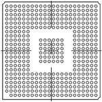
DLPC6401 DLPS031C–DECEMBER2013–REVISEDAUGUST2015 www.ti.com 5 Pin Configuration and Functions ZFFPACKAGE 419-PINBGA TOPVIEW 4 SubmitDocumentationFeedback Copyright©2013–2015,TexasInstrumentsIncorporated ProductFolderLinks:DLPC6401
DLPC6401 www.ti.com DLPS031C–DECEMBER2013–REVISEDAUGUST2015 PinFunctions PIN(1) I/O(2) INTERNALTERMINATION CLKSYSTEM DESCRIPTION NAME NO. POWER TYPE CONTROL Externalresetoutput,LOWtrue.Thisoutputis assertedlowimmediatelyuponassertingpower-up reset(POSENSE)lowandremainslowwhile POSENSEremainslow.EXT_ARSTZcontinuesto beheldlowafterthereleaseofpower-upreset(that is,POSENSEsethigh)untilreleasedbysoftware. EXT_ARST H20 VDD33 O1 Async EXT_ARSTZisalsoassertedlowapproximately5 µsafterthedetectionofaPWRGOODorany internally-generatedreset.Inallcases,itremains activeforaminimumof2msafterthereset conditionisreleasedbysoftware.Note,theASIC containsasoftwareregisterthatcanbeusedto independentlydrivethisoutput. PowerGoodisanactive-highsignalwithhysteresis thatisgeneratedbyanexternalpowersupplyor voltagemonitor.Ahighvalueindicatesallpoweris withinoperatingvoltagespecificationsandthe systemissafetoexititsresetstate.Atransitionfrom hightolowshouldindicatethatthecontrolleror DMDsupplyvoltagewilldropbelowtheirrated minimumlevelwithinthenext0.5ms(POSENSE mustremainactivehighduringthisinterval).Thisis anearlywarningofanimminentpowerloss PWRGOOD H19 VDDC I4 Async condition.Thiswarningisrequiredtoenhancelong- H termDMDreliability.ADMDparksequence, followedbyafullcontrollerreset,isperformedbythe DLPC6401whenPWRGOODgoeslowfora minimumof4µsprotectingtheDMD.Thisminimum de-assertiontimeisusedtoprotecttheinputfrom glitches.Followingthis,theDLPC6401isheldinits resetstateaslongasPWRGOODislow. PWRGOODmustbedrivenhighfortypical operation.TheDLPC6401deviceacknowledges PWRGOODasactiveafteritisdrivenhighfora minimumof625ns.Useshysteresis. Power-OnSenseisanactive-highinputsignalwith hysteresisthatisgeneratedbyanexternalvoltage monitorcircuit.POSENSEmustbedriveninactive POSENSE G21 I4 Async (low)whenanyofthecontrollersupplyvoltagesare H belowminimumoperatingvoltagespecifications. POSENSEmustbeactive(high)whenallcontroller supplyvoltagesremainaboveminimum specifications. PowerOnorPowerOffisanactive-highsignalthat indicatesthepowerofthesystem.PowerOnor PowerOffishighwhenthesystemisinpower-up POWER_ON_OFF N21 VDD33 B2 Async state,andlowwhenthesystemisinstandby.Power OnorPowerOffcanalsobeusedtopoweronoroff anexternalpowersupply. Priortotransferringpartofcodefromparallelflash contenttointernalmemory,theinternalmemoryis initializedandamemorytestisperformed.The INIT_DONE F19 VDD33 B2 Async resultofthistest(passorfail)isrecordedinthe systemstatus.Ifmemorytestfails,theinitialization processishalted.INIT_DONEisassertedtwiceto indicateanerrorsituation.SeeFigure12. Thissignalissampledduringpower-up.Ifthesignal I2C_ADDR_SEL F21 VDD33 B2 Async islow,theI2Caddressesare0x34and0x35.Ifthe signalislow,theI2Care0x3Aand0x3B. Requiresanexternalpullupto I2Cclock.Bidirectional,open-drainsignal.I2Cslave 3.3V.Theminimum I2C1_SCL J3 VDD33 B2 acceptablepullupvalueis N/A clockinputfromtheexternalprocessor.Thisbus supports400kHz. 1kΩ. Requiresanexternalpullupto I2Cdata.Bidirectional,open-drainsignal.I2Cslave 3.3V.Theminimum I2C1_SDA J4 VDD33 B2 acceptablepullupvalueis I2C1_SCL toacceptcommandortransferdatatoandfromthe externalprocessor.Thisbussupports400kHz. 1kΩ. (1) Forinstructionsonhandlingunusedpins,seeGeneralHandlingGuidelinesforUnusedCMOS-TypePins. (2) I/OType:I=Input,O=Output,B=Bidirectional,andH=Hysteresis.SeeTable1forsubscriptexplanation. Copyright©2013–2015,TexasInstrumentsIncorporated SubmitDocumentationFeedback 5 ProductFolderLinks:DLPC6401
DLPC6401 DLPS031C–DECEMBER2013–REVISEDAUGUST2015 www.ti.com PinFunctions(continued) PIN(1) I/O(2) INTERNALTERMINATION CLKSYSTEM DESCRIPTION NAME NO. POWER TYPE Requiresanexternalpullupto 3.3V.Theminimum I2Cbus0,clock;I2Cmasterforon-boardperipherals I2C0_SCL M2 VDD33 B8 acceptablepullupvalueis1 N/A suchastemperaturesensor.Thisbussupports400- kΩ.Thisinputisnot kHz,fast-modeoperation. 5-Vtolerant. Requiresanexternalpullupto 3.3V.Theminimum I2Cbus0,data;I2Cmasterforon-boardperipherals I2C0_SDA M3 VDD33 B8 acceptablepullupvalueis1 I2C0_SCL suchastemperaturesensor.Thisbussupports400- kΩ.Thisinputisnot kHz,fast-modeoperation. 5-Vtolerant. SYSTEMCLOCK Systemclockoscillatorinput(3.3-VLVCMOS).Note MOSC A14 VDD33 I10 N/A thattheMOSCmustbestableamaximumof25ms afterPOSENSEtransitionsfromhightolow. MOSCN A15 VDD33 O10 N/A MOSCcrystalreturn PORT1:PARALLELVIDEOANDGRAPHICSINPUT(3)(4)(5) P1A_CLK W15 VDD33 I4 Includesaninternalpulldown N/A Port1inputdatapixelwriteclock'A' P1B_CLK AB17 VDD33 I4 Includesaninternalpulldown N/A Port1inputdatapixelwriteclock'B' P1C_CLK Y16 VDD33 I4 Includesaninternalpulldown N/A Port1inputdatapixelwriteclock'C' P1_VSYNC Y15 VDD33 B1 Includesaninternalpulldown P1A_CLK Port1verticalsync.Useshysteresis H P1_HSYNC AB16 VDD33 B1 Includesaninternalpulldown P1A_CLK Port1horizontalsync.Useshysteresis H P1_DATEN AA16 VDD33 I4 Includesaninternalpulldown P1A_CLK Port1dataenable Port1fieldsync.Requiredforinterlacedsources P1_FIELD W14 VDD33 I4 Includesaninternalpulldown P1A_CLK only(andnotprogressive) P1_A_9 AB20 VDD33 I4 Includesaninternalpulldown P1A_CLK Port1Achannelinputpixeldata(bitweight128) P1_A_8 AA19 VDD33 I4 Includesaninternalpulldown P1A_CLK Port1Achannelinputpixeldata(bitweight64) P1_A_7 Y18 VDD33 I4 Includesaninternalpulldown P1A_CLK Port1Achannelinputpixeldata(bitweight32) P1_A_6 W17 VDD33 I4 Includesaninternalpulldown P1A_CLK Port1Achannelinputpixeldata(bitweight16) P1_A_5 AB19 VDD33 I4 Includesaninternalpulldown P1A_CLK Port1Achannelinputpixeldata(bitweight8) P1_A_4 AA18 VDD33 I4 Includesaninternalpulldown P1A_CLK Port1Achannelinputpixeldata(bitweight4) P1_A_3 Y17 VDD33 I4 Includesaninternalpulldown P1A_CLK Port1Achannelinputpixeldata(bitweight2) P1_A_2 AB18 VDD33 I4 Includesaninternalpulldown P1A_CLK Port1Achannelinputpixeldata(bitweight1) P1_A_1 W16 VDD33 I4 Includesaninternalpulldown P1A_CLK Port1Achannelinputpixeldata(bitweight0.5) P1_A_0 AA17 VDD33 I4 Includesaninternalpulldown P1A_CLK Port1Achannelinputpixeldata(bitweight0.25) P1_B_9 U21 VDD33 I4 Includesaninternalpulldown P1A_CLK Port1Bchannelinputpixeldata(bitweight128) P1_B_8 U20 VDD33 I4 Includesaninternalpulldown P1A_CLK Port1Bchannelinputpixeldata(bitweight64) P1_B_7 V22 VDD33 I4 Includesaninternalpulldown P1A_CLK Port1Bchannelinputpixeldata(bitweight32) P1_B_6 U19 VDD33 I4 Includesaninternalpulldown P1A_CLK Port1Bchannelinputpixeldata(bitweight16) P1_B_5 V21 VDD33 I4 Includesaninternalpulldown P1A_CLK Port1Bchannelinputpixeldata(bitweight8) P1_B_4 W22 VDD33 I4 Includesaninternalpulldown P1A_CLK Port1Bchannelinputpixeldata(bitweight4) P1_B_3 W21 VDD33 I4 Includesaninternalpulldown P1A_CLK Port1Bchannelinputpixeldata(bitweight2) P1_B_2 AA20 VDD33 I4 Includesaninternalpulldown P1A_CLK Port1Bchannelinputpixeldata(bitweight1) P1_B_1 Y19 VDD33 I4 Includesaninternalpulldown P1A_CLK Port1Bchannelinputpixeldata(bitweight0.5) P1_B_0 W18 VDD33 I4 Includesaninternalpulldown P1A_CLK Port1Bchannelinputpixeldata(bitweight0.25) P1_C_9 P21 VDD33 I4 Includesaninternalpulldown P1A_CLK Port1Cchannelinputpixeldata(bitweight128) P1_C_8 P22 VDD33 I4 Includesaninternalpulldown P1A_CLK Port1Cchannelinputpixeldata(bitweight64) (3) Port1canbeusedtosupportmultiplesourceoptionsforagivenproduct(thatis,HDMI,BT656).Todoso,thedatabusfromboth sourcecomponentsmustbeconnectedtothesameport1pinsandcontrolgiventotheDLPC6401totri-statetheinactivesource.Tying themtogetherlikethiscausessomesignaldegradationduetoreflectionsonthetri-statedpath. (4) TheA,B,andCinputdatachannelsofport1canbeinternallyswappedforoptimumboardlayout. (5) Sourcesfeedinglessthanthefull10-bitspercolorcomponentchannelshouldbeMSBjustifiedwhenconnectedtotheDLPC6401and LSBstiedoffto0.Forexample,an8-bitpercolorinputshouldbeconnectedtobits9:2ofthecorrespondingA,B,orCinputchannel. BT656are8or10bitsinwidth.IfaBT656-typeinputisused,thedatabitsmustbeMSBjustifiedaswiththeothertypesofinput sourcesoneitheroftheA,B,orCdatainputchannels. 6 SubmitDocumentationFeedback Copyright©2013–2015,TexasInstrumentsIncorporated ProductFolderLinks:DLPC6401
DLPC6401 www.ti.com DLPS031C–DECEMBER2013–REVISEDAUGUST2015 PinFunctions(continued) PIN(1) I/O(2) INTERNALTERMINATION CLKSYSTEM DESCRIPTION NAME NO. POWER TYPE P1_C_7 R19 VDD33 I4 Includesaninternalpulldown P1A_CLK Port1Cchannelinputpixeldata(bitweight32) P1_C_6 R20 VDD33 I4 Includesaninternalpulldown P1A_CLK Port1Cchannelinputpixeldata(bitweight16) P1_C_5 R21 VDD33 I4 Includesaninternalpulldown P1A_CLK Port1Cchannelinputpixeldata(bitweight8) P1_C_4 R22 VDD33 I4 Includesaninternalpulldown P1A_CLK Port1Cchannelinputpixeldata(bitweight4) P1_C_3 T21 VDD33 I4 Includesaninternalpulldown P1A_CLK Port1Cchannelinputpixeldata(bitweight2) P1_C_2 T20 VDD33 I4 Includesaninternalpulldown P1A_CLK Port1Cchannelinputpixeldata(bitweight1) P1_C_1 T19 VDD33 I4 Includesaninternalpulldown P1A_CLK Port1Cchannelinputpixeldata(bitweight0.5) P1_C_0 U22 VDD33 I4 Includesaninternalpulldown P1A_CLK Port1Cchannelinputpixeldata(bitweight0.25) PORT2:FPD-LINKCOMPATIBLEVIDEOANDGRAPHICSINPUT(6) Includesweakinternal Positivedifferentialinputsignalforclock,FPD-Link RCK_IN_P Y9 VDD33_FPD I5 pulldown N/A receiver Includesweakinternal Negativedifferentialinputsignalforclock,FPD-Link RCK_IN_N W9 VDD33_FPD I5 pulldown N/A receiver Includesweakinternal PositivedifferentialinputsignalfordatachannelA, RA_IN_P AB10 VDD33_FPD I5 pulldown RCK_IN FPD-Linkreceiver Includesweakinternal NegativedifferentialinputsignalfordatachannelA, RA_IN_N AA10 VDD33_FPD I5 pulldown RCK_IN FPD-Linkreceiver Includesweakinternal PositivedifferentialinputsignalfordatachannelB, RB_IN_P Y11 VDD33_FPD I5 pulldown RCK_IN FPD-Linkreceiver Includesweakinternal NegativedifferentialinputsignalfordatachannelB, RB_IN_N W11 VDD33_FPD I5 pulldown RCK_IN FPD-Linkreceiver Includesweakinternal PositivedifferentialinputsignalfordatachannelC, RC_IN_P AB12 VDD33_FPD I5 pulldown RCK_IN FPD-Linkreceiver Includesweakinternal NegativedifferentialinputsignalfordatachannelC, RC_IN_N AA12 VDD33_FPD I5 pulldown RCK_IN FPD-Linkreceiver Includesweakinternal PositivedifferentialinputsignalfordatachannelD, RD_IN_P Y13 VDD33_FPD I5 pulldown RCK_IN FPD-Linkreceiver Includesweakinternal NegativedifferentialinputsignalfordatachannelD, RD_IN_N W13 VDD33_FPD I5 pulldown RCK_IN FPD-Linkreceiver Includesweakinternal PositivedifferentialinputsignalfordatachannelE, RE_IN_P AB14 VDD33_FPD I5 pulldown RCK_IN FPD-Linkreceiver Includesweakinternal NegativedifferentialinputsignalfordatachannelE, RE_IN_N AA14 VDD33_FPD I5 pulldown RCK_IN FPD-Linkreceiver (6) Port2isasingle-channelFPD-Linkcompatibleinputinterface.FPD-LinkisadefactoindustrystandardFPDinterface,whichusesthe high-bandwidthcapabilitiesofLVDSsignalingtoserializevideoandgraphicsdatadowntoacouplewirestoprovidealow-wirecount andlow-EMIinterface.Port2supportssourceratesuptoamaximumeffectiveclockof90MHz.Theport2inputpixeldatamustadhere tooneoffoursupporteddatamappingformats(seeTable2).Giventhatport2inputscontainweakpulldownresistors,theycanbeleft floatingwhennotused. Copyright©2013–2015,TexasInstrumentsIncorporated SubmitDocumentationFeedback 7 ProductFolderLinks:DLPC6401
DLPC6401 DLPS031C–DECEMBER2013–REVISEDAUGUST2015 www.ti.com PinFunctions(continued) PIN(1) I/O(2) INTERNALTERMINATION CLKSYSTEM DESCRIPTION NAME NO. POWER TYPE DMDINTERFACE DMD_D0 A8 DMD_D1 B8 DMD_D2 C8 DMD_D3 D8 DMD_D4 B11 DMD_D5 C11 DMD_D6 D11 DMD_D7 E11 DMD_D8 C7 DMD_D9 B10 DMD_D10 E7 DMDdatapins.DMDdatapinsareDDRsignalsthat areclockedonbothedgesofDMD_DCLK. DMD_D11 D10 VDD_DMD O7 DMD_DCLK All24DMDdatasignalsareusetointerfacetothe DLP4500. DMD_D12 A6 DMD_D13 A12 DMD_D14 B12 DMD_D15 C12 DMD_D16 D12 DMD_D17 B7 DMD_D18 A10 DMD_D19 D7 DMD_D20 B6 DMD_D21 E9 DMD_D22 C10 DMD_D23 C6 DMD_DCLK A9 VDD_DMD O7 N/A DMDdataclock(DDR) DMD_LOADB B9 VDD_DMD O7 DMD_DCLK DMDdataloadsignal(active-low) DMD_SCTRL C9 VDD_DMD O7 DMD_DCLK DMDdataserialcontrolsignal DMD_TRC D9 VDD_DMD O7 DMD_DCLK DMDdatatoggleratecontrol DMD_DRC_BUS D5 VDD_DMD O7 DMD_SAC_CLK DMDresetcontrolbusdata DMD_DRC_STRB C5 VDD_DMD O7 DMD_SAC_CLK DMDresetcontrolbusstrobe Requiresa30to51-kΩ DMD_DRC_OE B5 VDD_DMD O7 externalpullupresistorto Async DMDresetcontrolenable(activelow) VDD_DMD. DMD_SAC_BUS D6 VDD_DMD O7 DMD_SAC_CLK DMDstepped-addresscontrolbusdata DMD_SAC_CLK A5 VDD_DMD O7 N/A DMDstepped-addresscontrolbusclock DMDPowerEnablecontrol.Thissignalindicatesto DMD_PWR_EN G20 VDD_DMD O2 Async anexternalregulatorthattheDMDispowered. DMDdrivestrengthadjustmentprecisionreference. EXRES A3 O Async A±1%externalprecisionresistorshouldbe connectedtothispin. FLASHINTERFACE Reservedforfutureuse.OnthePCB,connectto PM_CS_0 U3 VDD33 O2 Async VDD33throughapullupresistor. PM_CS_1 U2 VDD33 O2 Async Bootflash(activelow).Requiredforbootmemory Reservedforfutureuse.OnthePCB,connectto PM_CS_2 U1 VDD33 O2 Async VDD33throughapullupresistor. 8 SubmitDocumentationFeedback Copyright©2013–2015,TexasInstrumentsIncorporated ProductFolderLinks:DLPC6401
DLPC6401 www.ti.com DLPS031C–DECEMBER2013–REVISEDAUGUST2015 PinFunctions(continued) PIN(1) I/O(2) INTERNALTERMINATION CLKSYSTEM DESCRIPTION NAME NO. POWER TYPE PM_ADDR_22 V3 B2 PM_ADDR_21 W1 PM_ADDR_20 W2 PM_ADDR_19 Y1 PM_ADDR_18 AB2 PM_ADDR_17 AA3 PM_ADDR_16 Y4 PM_ADDR_15 W5 PM_ADDR_14 AB3 PM_ADDR_13 AA4 PM_ADDR_12 Y5 PM_ADDR_11 W6 VDD33 O2 Async Flashmemoryaddressbit PM_ADDR_10 AB4 PM_ADDR_9 AA5 PM_ADDR_8 Y6 PM_ADDR_7 W7 PM_ADDR_6 AB5 PM_ADDR_5 AA6 PM_ADDR_4 Y7 PM_ADDR_3 AB6 PM_ADDR_2 W8 PM_ADDR_1 AA7 PM_ADDR_0 AB7 PM_WE V2 VDD33 O2 Async Writeenable(activelow) PM_OE U4 VDD33 O2 Async Outputenable(activelow) PM_BLS_1 AA8 VDD33 O2 Async Upperbyte(15:8)enable PM_BLS_0 AB8 VDD33 O2 Async Lowerbyte(7:0)enable PM_DATA_15 M1 PM_DATA_14 N1 PM_DATA_13 N2 PM_DATA_12 N3 VDD33 B2 Async Databits,upperbyte PM_DATA_11 N4 PM_DATA_10 P1 PM_DATA_9 P2 PM_DATA_8 P3 PM_DATA_7 P4 PM_DATA_6 R2 PM_DATA_5 R3 PM_DATA_4 R4 VDD33 B2 Async Databits,lowerbyte PM_DATA_3 T1 PM_DATA_2 T2 PM_DATA_1 T3 PM_DATA_0 T4 LEDDRIVERINTERFACE LEDR_PWM K2 LEDredPWMoutputenablecontrol LEDG_PWM K3 VDD33 O2 Async LEDgreenPWMoutputenablecontrol LEDB_PWM K4 LEDbluePWMoutputenablecontrol LEDR_EN L3 LEDredPWMoutput LEDG_EN L4 VDD33 O2 Async LEDgreenPWMoutput LEDB_EN K1 LEDbluePWMoutput Copyright©2013–2015,TexasInstrumentsIncorporated SubmitDocumentationFeedback 9 ProductFolderLinks:DLPC6401
DLPC6401 DLPS031C–DECEMBER2013–REVISEDAUGUST2015 www.ti.com PinFunctions(continued) PIN(1) I/O(2) INTERNALTERMINATION CLKSYSTEM DESCRIPTION NAME NO. POWER TYPE PERIPHERALINTERFACE UART_TXD L19 VDD33 O2 Async Transmitdataoutput.Reservedfordebugmessages UART_RXD L21 VDD33 I4 Async Receivedatainput.Reservedfordebugmessages Readytosendhardwareflowcontroloutput. UART_RTS M19 VDD33 O2 Async Reservedfordebugmessages Cleartosendhardwareflowcontrolinput.Reserved UART_CTS L20 VDD33 I4 Async fordebugmessages GENERALPURPOSEI/O(GPIO)(7) GPIO_37 K21 VDD33 B2 Async None GPIO_36 G1 VDD33 B2 Async None GPIO_35 H4 VDD33 B2 Async None GPIO_34 H3 VDD33 B2 Async None GPIO_33 H2 VDD33 B2 Async None GPIO_32 F22 VDD33 B2 Async None GPIO_31 G19 VDD33 B2 Async None GPIO_29 F20 VDD33 B2 Async None GPIO_28 E22 VDD33 B2 Async None GPIO_27 E21 VDD33 B2 Async None GPIO_25 D22 VDD33 B2 Async None GPIO_24 E20 VDD33 B2 Async None GPIO_23 D21 VDD33 B2 Async None GPIO_21 N20 VDD33 B2 Async None GPIO_20 N19 VDD33 B2 Async None GPIO_19 D18 VDD33 B2 Async None GPIO_18 C18 VDD33 B2 Async None GPIO_15 B19 VDD33 B2 Async None GPIO_14 B18 VDD33 B2 Async None GPIO_13 L2 VDD33 B2 Async None GPIO_12 M4 VDD33 B2 Async None GPIO_11 A19 VDD33 B2 Async None GPIO_10 C17 VDD33 B2 Async None GPIO_06 A18 VDD33 B2 Async None GPIO_05 D16 VDD33 B2 Async None GPIO_04 C16 VDD33 B2 Async None GPIO_03 B16 VDD33 B2 Async None GPIO_02 A17 VDD33 B2 Async None GPIO_00 C15 VDD33 B2 Async None OTHERINTERFACES Feedbackfromfantoindicatefanisconnectedand FAN_LOCKED B17 VDD33 B2 Async running FAN_PWM D15 VDD33 B2 Async FanPWMspeedcontrol BOARDLEVELTESTANDDEBUG TDI P18 VDD33 I4 Includesinternalpullup TCK JTAGserialdatain(8) TCK R18 VDD33 I4 Includesinternalpullup N/A JTAGserialdataclock(8) TMS1 V15 VDD33 I4 Includesinternalpullup TCK JTAGtestmodeselect(8) TDO1 L18 VDD33 O1 TCK JTAGserialdataout(8) (7) GPIOsignalsmustbeconfiguredbysoftwareforinput,output,bidirectional,oropen-drain.SomeGPIOshaveoneormorealternateuse modes,whicharealsosoftwareconfigurable.TheresetdefaultforalloptionalGPIOsisasaninputsignal.However,anyalternate functionconnectedtotheseGPIOpinswiththeexceptionofgeneral-purposeclocksandPWMgeneration,arereset.Anexternalpullup tothe3.3-Vsupplyisrequiredforeachsignalconfiguredasopen-drain.Externalpulluporpulldownresistorsmayberequiredtoensure stableoperationbeforesoftwareisabletoconfiguretheseports. (8) AllJTAGsignalsareLVCMOS-compatible. 10 SubmitDocumentationFeedback Copyright©2013–2015,TexasInstrumentsIncorporated ProductFolderLinks:DLPC6401
DLPC6401 www.ti.com DLPS031C–DECEMBER2013–REVISEDAUGUST2015 PinFunctions(continued) PIN(1) I/O(2) INTERNALTERMINATION CLKSYSTEM DESCRIPTION NAME NO. POWER TYPE JTAG,RESET(activelow).Thispinshouldbepulled high(orleftunconnected)whentheJTAGinterface TRST V17 VDD33 I4 Includesinternalpullup Async isinuseforboundaryscan.Connectthispinto H groundotherwise.Failuretotiethispinlowduring normaloperationcausesstartupandinitialization problems.(8) RTCK G18 VDD33 O2 N/A JTAGreturnclock(9) Includesinternalpulldown. ICTSEN V6 VDD33 I4 Externalpulldown Async ICTri-StateEnable(activehigh).Assertinghightri- H recommendedforadded statesalloutputsexcepttheJTAGinterface. protection. (9) Forinstructionsonhandlingunusedpins,seeGeneralHandlingGuidelinesforUnusedCMOS-TypePins. FunctionalPinDescriptions(ReservedPins) PIN(1) I/O (2) CLK INTERNALTERMINATION DESCRIPTION NAME NO. POWER TYPE SYSTEM I RESERVED V7 VDD33 4 Includesinternalpulldown N/A ConnectdirectlytogroundonthePCB. H N22,M22, RESERVED VDD33 I Includesaninternalpulldown N/A P19,P20 4 Reserved(1) RESERVED V16 VDD33 I Includesaninternalpullup N/A 4 RESERVED D1,J2 VDD33 I N/A 4 F1,F2,G2, RESERVED VDD33 O Includesinternalpulldown N/A G3,G4 2 RESERVED F3,J1,M21 VDD33 O N/A Leavethesepinsunconnected(1) 2 H20,M18, RESERVED VDD33 O N/A M20 1 H21,H22, J19,J20, RESERVED VDD33 B Includesinternalpulldown N/A J21,J22, 2 Reserved(1) K19,K20 RESERVED C1,D2,F4 VDD33 B N/A 2 RESERVED E3,E2 VDD33 — Async Reserved (1) Forinstructionsonhandlingunusedpins,seeGeneralHandlingGuidelinesforUnusedCMOS-TypePins. (2) I/OType:Iindicatesinput,Oindicatesoutput,Bindicatesbidirectional,andHindicateshysteresis.SeeTable1forsubscript explanation. Table1.I/OTypeSubscriptDefinition I/O ESDSTRUCTURE SUBSCRIPT DESCRIPTION 1 3.3-VLVCMOSI/Obuffer,with4-mAdrive ESDdiodetoVDD33andGND 2 3.3-VLVCMOSI/Obuffer,with8-mAdrive ESDdiodetoVDD33andGND 3 3.3-VLVCMOSI/Obuffer,with12-mAdrive ESDdiodetoVDD33andGND 4 3.3-VLVCMOSreceiver ESDdiodetoVDD33andGND 5 3.3-VLVDSreceiver(FPD-LinkI/F) ESDdiodetoVDD33andGND 6 None N/A 7 1.9-VLPDDRoutputbuffer(DMDI/F) ESDdiodetoVDD_DMDandGND 8 3.3-VI2Cwith12-mAsink ESDdiodetoVDD33andGND 10 OSC3.3-VI/OcompatibleLVCMOS ESDdiodetoVDD33andGND Copyright©2013–2015,TexasInstrumentsIncorporated SubmitDocumentationFeedback 11 ProductFolderLinks:DLPC6401
DLPC6401 DLPS031C–DECEMBER2013–REVISEDAUGUST2015 www.ti.com 6 Specifications 6.1 Absolute Maximum Ratings overrecommendedoperatingfree-airtemperature(unlessotherwisenoted) (1) MIN MAX UNIT ELECTRICAL VDDC(core1.2-Vpower) –0.5 1.7 VDD33(CMOSI/O) –0.5 3.8 VDD_DMD(DMDdriverpower) –0.5 2.3 VDD12_FPD(FPD-LinkLVDSinterface1.2-Vpower) –0.5 1.7 Supplyvoltage(2) VDD33_FPD(FPD-LinkLVDSinterface3.3-Vpower) –0.5 3.8 VDD12_PLLD(DDRclockgenerator–digital) –0.5 1.7 VDD12_PLLM(masterclockgenerator–digital) –0.5 1.7 VDD_18_PLLD(DDRclockgenerator–analog) –0.5 2.3 V VDD_18_PLLM(masterclockgenerator–analog) –0.5 2.3 OSC(BC1850) –0.3 3.6 LVCMOS(BT3350) –0.5 3.6 V Inputvoltage(3) I I2C(BT3350) –0.5 3.6 LVDS(BT3350) –0.5 3.6 DMDLPDDR(BC1850) –0.3 2.0 V Outputvoltage LVCMOS(BT3350) –0.5 3.6 O I2C(BT3350) –0.5 3.6 ENVIRONMENTAL T Operatingjunctiontemperature 0 115 °C J T Storagetemperature –40 125 °C stg (1) StressesbeyondthoselistedunderAbsoluteMaximumRatingsmaycausepermanentdamagetothedevice.Thesearestressratings only,whichdonotimplyfunctionaloperationofthedeviceattheseoranyotherconditionsbeyondthoseindicatedunderRecommended OperatingConditions.Exposuretoabsolute-maximum-ratedconditionsforextendedperiodsmayaffectdevicereliability. (2) AllvoltagevaluesarewithrespecttoGND. (3) Appliestoexternalinputandbidirectionalbuffers. 6.2 ESD Ratings VALUE UNIT Humanbodymodel(HBM),perANSI/ESDA/JEDECJS-001,allpins(1) ±2000 Electrostatic Chargeddevicemodel(CDM),perJEDECspecificationJESD22-C101,all V(ESD) discharge pins(2) ±500 V Machinemodel(MM) ±150 (1) JEDECdocumentJEP155statesthat500-VHBMallowssafemanufacturingwithastandardESDcontrolprocess. (2) JEDECdocumentJEP157statesthat250-VCDMallowssafemanufacturingwithastandardESDcontrolprocess. 12 SubmitDocumentationFeedback Copyright©2013–2015,TexasInstrumentsIncorporated ProductFolderLinks:DLPC6401
DLPC6401 www.ti.com DLPS031C–DECEMBER2013–REVISEDAUGUST2015 6.3 Recommended Operating Conditions overoperatingfree-airtemperaturerange(unlessotherwisenoted) I/O(1) MIN NOM MAX UNIT VDD33 3.3-Vsupplyvoltage,I/O 3.135 3.3 3.465 V VDD_DMD 1.9-Vsupplyvoltage,I/O 1.8 1.9 2 V VDD_18_PLLD 1.8-Vsupplyvoltage,PLLanalog 1.71 1.8 1.89 V VDD_18_PLLM 1.8-Vsupplyvoltage,PLLanalog 1.71 1.8 1.89 V VDD12 1.2-Vsupplyvoltage,corelogic 1.116 1.2 1.26 V VDD12_PLLD 1.2-Vsupplyvoltage,PLLdigital 1.116 1.2 1.26 V VDD12_PLLM 1.2-Vsupplyvoltage,PLLdigital 1.116 1.2 1.26 V OSC(10) 0 VDD33 3.3-VLVCMOS(1,2,3,4) 0 VDD33 V Inputvoltage V I 3.3-VI2C(8) 0 VDD33 3.3-VLVDS(5) 0.6 2.2 3.3-VLVCMOS(1,2,3,4) 0 VDD33 V Outputvoltage 3.3-VI2C(8) 0 VDD33 V O 1.9-VLPDDR(7) 0 VDD_DMD T Operatingambienttemperaturerange See (2) 0 55 °C A T Operatingtop-centercasetemperature See (3)(4) 0 104 °C C T Operatingjunctiontemperature 0 105 °C J (1) ThenumberinsideeachparenthesisfortheI/OreferstothetypedefinedintheI/Otypesubscriptdefinitionsection. (2) Assumesaminimum1-m/sairflowalongwiththeJEDECthermalresistanceandassociatedconditionsaslistedwww.ti.com/packaging. Thus,thisisanapproximatevaluethatvarieswithenvironmentandPCBdesign. (3) Maximumthermalvaluesassumemaximumpowerof3W. (4) Assumeψ equals0.33C/W. JT 6.4 Thermal Information(1) DLPC6401 THERMALMETRIC(1) ZFF(BGA) UNIT 419PINS ψ Junction-to-topcharacterizationparameter 0.33 °C/W JT (1) Formoreinformationabouttraditionalandnewthermalmetrics,seetheSemiconductorandICPackageThermalMetricsApplication Report,SPRA953. Copyright©2013–2015,TexasInstrumentsIncorporated SubmitDocumentationFeedback 13 ProductFolderLinks:DLPC6401
DLPC6401 DLPS031C–DECEMBER2013–REVISEDAUGUST2015 www.ti.com 6.5 Electrical Characteristics(1) overoperatingfree-airtemperaturerange(unlessotherwisenoted) PARAMETER TESTCONDITIONS MIN TYP MAX UNIT OSC(10) 2 High-levelinput VIH thresholdvoltage 3.3-VLVCMOS(1,2,3,4) 2 V 3.3-VI2C(8) 2.4 OSC(10) 0.8 Low-levelinput VIL thresholdvoltage 3.3-VLVCMOS(1,2,3,4) 0.8 V 3.3-VI2C(8) 1 Receiverinput RI 3.3-VLVDS(5) VDDH=3.3V 90 110 132 Ω impedance Inputdifferential Vidth 3.3-VLVDS(5) –200 200 mV threshold Absoluteinput |Vid| 3.3-VLVDS(5) 200 600 mV differentialvoltage Atminimumabsolute 3.3-VLVDS(5) 0.7 2.1 Inputcommonmode inputdifferentialvoltage VICM V voltagerange Atmaxabsoluteinput 3.3-VLVDS(5) 0.9 1.9 differentialvoltage 3.3-VLVCMOS(1,2,3,4) 400 VHYS Hysteresis(VT+–VT–) mV 3.3-VI2C(8) 550 High-leveloutput 3.3-VLVCMOS(1,2,3) IOH=Maxrated 2.8 VOH voltage 1.9-VDMDLPDDR(7) IOH=–0.1mA 0.9×VDD_DMD V 1.9-VDMDLPDDR(7) IOL=0.1mA 0.1×VDD_DMD Low-leveloutput VOL voltage 3.3-VLVCMOS(1,2,3) IOL=Maxrated 0.4 V 3.3-VI2C(8) IOL=3-mAsink 0.4 OSC(10) 10.0 3.3-VLVCMOS(1to4)(without internalpulldown) VIH=VDD33 10 IIH High-levelinputcurrent 3.3VLVCMOS(1to4)(with µA internalpulldown) VIH=VDD33 200 3.3VI2C(8) VIH=VDD33 10 OSC(10) –10.0 3.3-VLVCMOS(1to4)(without internalpullup) VOH=VDD33 –10 IIL Low-levelinputcurrent 3.3-VLVCMOS(1to4)(with µA internalpullup) VOH=VDD33 –200 3.3-VI2C(8) VOH=VDD33 –10 1.9-VDMDLPDDR(7) VO=1.5V –4 High-leveloutput 3.3-VLVCMOS(1) VO=2.4V –4 IOH current 3.3-VLVCMOS(2) VO=2.4V –8 mA 3.3-VLVCMOS(3) VO=2.4V –12 1.9-VDMDLPDDR(7) VO=0.4V 4 3.3-VLVCMOS(1) VO=0.4V 4 Low-leveloutput IOL current 3.3-VLVCMOS(2) VO=0.4V 8 mA 3.3-VLVCMOS(3) VO=0.4V 12 3.3-VI2C(8) 3 High-impedance 3.3-VLVCMOS(1,2,3) –10 10 IOZ leakagecurrent 3.3-VI2C(8) –10 10 µA 3.3-VLVCMOS(2) 2.8 3.3 4 Inputcapacitance CI (includingpackage) 3.3-VLVCMOS(4) 2.7 3.4 4.2 pF 3.3-VI2C(8) 3 3.2 3.5 (1) ThenumberinsideeachparenthesisfortheI/OreferstothetypedefinedinTable1. 14 SubmitDocumentationFeedback Copyright©2013–2015,TexasInstrumentsIncorporated ProductFolderLinks:DLPC6401
DLPC6401 www.ti.com DLPS031C–DECEMBER2013–REVISEDAUGUST2015 6.6 Electrical Characteristics (Normal Mode) overoperatingfree-airtemperaturerange(unlessotherwisenoted) PARAMETER TESTCONDITION(1) MIN TYP MAX(2) UNIT I Supplyvoltage,1.2-Vcorepower Normalmode 600 1020 mA CC12 Supplyvoltage,1.9-VI/Opower(DMDLPDDR) Normalmode 30 50 mA ICC19_DMD I Supplyvoltage,3.3-V(I/O)power Normalmode 40 70 mA CC33 I FPD-LinkLVDSI/Fsupplyvoltage,1.2-Vpower Normalmode 60 100 mA CC12_FPD I FPD-LinkLVDSI/Fsupplyvoltage,3.3-Vpower Normalmode 50 85 mA CC33_FPD I Supplyvoltage,PLLdigitalpower(1.2V) Normalmode 9 15 mA CC12_PLLD Supplyvoltage,masterclockgeneratorPLLdigital I Normalmode 9 15 mA CC12_PLLM power(1.2V) I Supplyvoltage,PLLanalogpower(1.8V) Normalmode 10 16 mA CC18_PLLD Supplyvoltage,masterclockgeneratorPLLanalog I Normalmode 10 16 mA CC18_PLLM power(1.8V) P Totalpower Normalmode 1225 2200 mW TOT (1) NormalmodereferstoASICoperationduringfullfunctionality,activeproductoperation.Typicalvaluescorrespondtopowerdissipated onnominalprocessdevicesoperatingatnominalvoltageand70°Cjunctiontemperature(approximately25°Cambient)displayingtypical video-graphicscontentfromahigh-frequencysource.Maximimvaluescorrespondtopowerdissipatedonfastprocessdevices operatingathighvoltageand105°Cjunctiontemperature(approximately55°Cambient)displayingtypicalvideo-graphicscontentfroma high-frequencysource.Theincreasedpowerdissipationobservedonfastprocessdevicesoperatedatmaximumrecommended temperatureisprimarilyaresultofincreasedleakagecurrent. (2) MaximumpowervaluesareestimatesandmaynotreflecttheactualfinalpowerconsumptionofDLPC6401ASIC. 6.7 System Oscillators Timing Requirements overoperatingfree-airtemperaturerange(unlessotherwisenoted) MIN MAX UNIT ƒ Clockfrequency,MOSC(1) 31.9968 32.0032 MHz clock t Cycletime,MOSC(1) 31.188 31.256 ns c t Pulseduration(2),MOSC,high 50%to50%referencepoints(signal) 12.5 ns w(H) t Pulseduration(2),MOSC,low 50%to50%referencepoints(signal) 12.5 ns w(L) t Transitiontime(2),MOSC,t =t /t 20%to80%referencepoints(signal) 7.5 ns t t f r Periodjitter(2),MOSC(thatis,thedeviationinperiodfromidealperiodduesolelytohigh-frequency t –100 100 ps jp jitter–notspreadspectrumclocking) (1) ThefrequencyrangeforMOSCis32MHzwith±100PPMaccuracy.(Thisincludesimpacttoaccuracyduetoaging,temperature,and trimsensitivity.)TheMOSCinputcannotsupportspreadspectrumclockspreading. (2) Appliesonlywhendrivenbyanexternaldigitaloscillator. Copyright©2013–2015,TexasInstrumentsIncorporated SubmitDocumentationFeedback 15 ProductFolderLinks:DLPC6401
DLPC6401 DLPS031C–DECEMBER2013–REVISEDAUGUST2015 www.ti.com 6.8 Test and Reset Timing Requirements MIN MAX UNIT t Pulseduration,inactivelow,PWRGOOD 50%to50%referencepoints(signal) 4 µs W1(L) t Transitiontime,PWRGOOD,t =t /t 20%to80%referencepoints(signal) 625 µs t1 t1 f r t Pulseduration,inactivelow,POSENSE 50%to50%referencepoints(signal) 500 µs W2(L) t Transitiontime,POSENSE,t =t /t 20%to80%referencepoints(signal) 1 µs t2 t2 f r t Powerholdtime,POSENSEremainsactiveafter 20%to80%referencepoints(signal) 500 µs PH PWGOODisdeasserted 6.9 JTAG Interface: I/O Boundary Scan Application Timing Requirements MIN MAX UNIT ƒ Clockfrequency,TCK 10 MHz clock t Cycletime,TCK 100 ns C t Pulseduration,high 50%to50%referencepoints(signal) 40 ns W(H) t Pulseduration,low 50%to50%referencepoints(signal) 40 ns W(L) t Transitiontime,t =t /t 20%to80%referencepoints(signal) 5 ns t t f r t Setuptime,TDIvalidbeforeTCK↑ 8 ns SU t Holdtime,TDIvalidafterTCK↑ 2 ns h t Setuptime,TMS1validbeforeTCK↑ 8 ns SU t Holdtime,TMS1validafterTCK↑ 2 ns h 16 SubmitDocumentationFeedback Copyright©2013–2015,TexasInstrumentsIncorporated ProductFolderLinks:DLPC6401
DLPC6401 www.ti.com DLPS031C–DECEMBER2013–REVISEDAUGUST2015 6.10 Port 1 Input Pixel Interface Timing Requirements MIN MAX UNIT ƒ Clockfrequency,P1A_CLK,P1B_CLK,P1C_CLK 12 150 MHz clock t Cycletime,P1A_CLK,P1B_CLK,P1C_CLK 6.666 83.33 ns c t Pulseduration,high 50%to50%referencepoints(signal) 2.3 ns w(H) t Pulseduration,low 50%to50%referencepoints(signal) 2.3 ns w(L) t Clockperiodjitter,P1A_CLK,P1B_CLK,P1C_CLK Maxƒ See (1) ps jp (thatis,thedeviationinperiodfromidealperiod) clock t Transitiontime,t =t /t,P1A_CLK,P1B_CLK,P1C_CLK 20%to80%referencepoints(signal) 0.6 2 ns t t f r Transitiontime,t =t /t,P1_A(9-0),P1_B(9-0),P1_C(9- t t f r 20%to80%referencepoints(signal) 0.6 3 ns t 0),P1_HSYNC,P1_VSYNC,P1_DATEN Transitiontime,t =t /t,ALF_HSYNC,ALF_VSYNC, tt ALF_CSYNC(2) t f r 20%to80%referencepoints(signal) 0.6 3 ns SETUPANDHOLDTIMES(3) t Setuptime,P1_A(9-0),validbeforeP1x_CLK↑↓ 0.8 ns su t Holdtime,P1_A(9-0),validafterP1x_CLK↑↓ 0.8 ns h t Setuptime,P1_B(9-0),validbeforeP1x_CLK↑↓ 0.8 ns su t Holdtime,P1_B(9-0),validafterP1x_CLK↑↓ 0.8 ns h t Setuptime,P1_C(9-0),validbeforeP1x_CLK↑↓ 0.8 ns su t Holdtime,P1_C(9-0),validafterP1x_CLK↑↓ 0.8 ns h t Setuptime,P1_VSYNC,validbeforeP1x_CLK↑↓ 0.8 ns su t Holdtime,P1_VSYNC,validafterP1x_CLK↑↓ 0.8 ns h t Setuptime,P1_HSYNC,validbeforeP1x_CLK↑↓ 0.8 ns su t Holdtime,P1_HSYNC,validafterP1x_CLK↑↓ 0.8 ns h t Setuptime,P1_FIELD,validbeforeP1x_CLK↑↓ 0.8 ns su t Holdtime,P1_FIELD,validafterP1x_CLK↑↓ 0.8 ns h t Setuptime,P1_DATEN,validbeforeP1x_CLK↑↓ 0.8 ns su t Holdtime,P1_DATEN,validafterP1x_CLK↑↓ 0.8 ns h (1) Usethefollowingformulatoobtainthejitter:Maximumclockjitter=±[(1/ƒ )–5414ps]. clock (2) ALF_CSYNC,ALF_VSYNCandALF_HSYNCareasynchronoussignals. (3) Setupandholdtimesshouldbeconsideredthesameregardlessofclockused[P1A_CLK,P1B_CLK,P1C_CLK]. 6.11 Port 2 Input Pixel Interface (FPD-Link Compatible LVDS Input) Timing Requirements(1)(2)(3)(4)(5)(6) MIN MAX UNIT ƒ Clockfrequency,P2_CLK(LVDSinputclock) 20 90 MHz clock t Cycletime,P2_CLK(LVDSinputclock) 11.1 50 ns c Clockordataslewrate(ƒ <90MHz) 0.3 V/ns pxck t slew Clockordataslewrate(ƒ >90MHz) 0.5 V/ns pxck t Linkstart-uptime(internal) 1 ms startup (1) MinimizecrosstalkandmatchtracesonthePCBascloseaspossible. (2) Maintainthecommonmodevoltageascloseto1.2Vaspossible. (3) Maintaintheabsoluteinputdifferentialvoltageashighaspossible. (4) TheLVDSopeninputdetectionisrelatedtoalowcommonmodevoltageonly.Itisnotrelatedtoalow-differentialswing. (5) LVDSpower3.3-Vsupply(VDD33_FPD)noiselevelshouldbebelow100mV . PP (6) LVDSpower1.2-Vsupply(VDD12_FPD)noiselevelshouldbebelow60mV . PP Copyright©2013–2015,TexasInstrumentsIncorporated SubmitDocumentationFeedback 17 ProductFolderLinks:DLPC6401
DLPC6401 DLPS031C–DECEMBER2013–REVISEDAUGUST2015 www.ti.com 6.12 Synchronous Serial Port (SSP) Interface Timing Requirements MIN MAX UNIT t Setuptime,SSP0_RXDvalidbeforeSSP0_CLK↓ 10 ns su t Holdtime,SSP0_RXDvalidafterSSP0_CLK↓ 10 ns h t Transitiontime(1),SSP0_RXD,t =t /t 4 ns t t f r t Setuptime,SSP1_RXDvalidbeforeSSP1_CLK↓ 10 ns su t Holdtime,SSP1_RXDvalidafterSSP1_CLK↓ 10 ns h t Transitiontime(1),SSP1_RXD,t =t /t 4 ns t t f r (1) 20%to80%referencepoints(signal) 6.13 Programmable Output Clocks Switching Characteristics overoperatingfree-airtemperaturerange,C (mintiming)=5pF,C (maxtiming)=50pF(unlessotherwisenoted)(see L L Figure5) FROM PARAMETER TO(OUTPUT) MIN MAX UNIT (INPUT) ƒ Clockfrequency,OCLKC(1) N/A OCLKC 0.7759 48 MHz clock t Cycletime,OCLKC(1) N/A OCLKC 20.83 1288.8 ns c t Pulseduration,high50%to50%referencepoints(signal) N/A OCLKC (t /2)–2 ns w(H) c t Pulseduration,low(2)50%to50%referencepoints(signal) N/A OCLKC (t /2)–2 ns w(L) c ƒ Clockfrequency,OCLKD(1) N/A OCLKD 0.7759 48 MHz clock t Cycletime,OCLKD N/A OCLKD 20.83 1288.8 ns c t Pulseduration,high(2)50%to50%referencepoints(signal) N/A OCLKD (t /2)–2 ns w(H) c t Pulseduration,low(2)50%to50%referencepoints(signal) N/A OCLKD (t /2)–2 ns w(L) c ƒ Clockfrequency,OCLKE(1) N/A OCLKE 0.7759 48 MHz clock t Cycletime,OCLKE N/A OCLKE 20.83 1288.8 ns c t Pulseduration,high(2)50%to50%referencepoints(signal) N/A OCLKE (t /2)–2 ns w(H) c t Pulseduration,low(2)50%to50%referencepoints(signal) N/A OCLKE (t /2)–2 ns w(L) c (1) ThefrequencyofOCLKCthroughOCLKEisprogrammable. (2) ThedutycycleofOCLKCthroughOCLKEiswithin±2nsof50%. 18 SubmitDocumentationFeedback Copyright©2013–2015,TexasInstrumentsIncorporated ProductFolderLinks:DLPC6401
DLPC6401 www.ti.com DLPS031C–DECEMBER2013–REVISEDAUGUST2015 6.14 Synchronous Serial Port (SSP) Interface Switching Characteristics overrecommendedoperatingconditions,C (mintiming)=5pF,C (maxtiming)=35pF(unlessotherwisenoted)(see L L Figure10) PARAMETER FROM(INPUT) TO(OUTPUT) MIN MAX UNIT ƒ Clockfrequency,SSP0_CLK (1)(2) N/A SSP0_CLK 0.287 9333 kHz clock t Cycletime,SSP0_CLK N/A SSP0_CLK 0.107 3483 us c t Pulseduration,high50%to50%referencepoints N/A SSP0_CLK 48 ns w(H) (signal) t Pulseduration,low50%to50%referencepoints N/A SSP0_CLK 48 ns w(L) (signal) t Outputpropagation,clocktoQ,SSP0_TXD SSP0_CLK↑ SSP0_TXD –5 5 ns pd ƒ Clockfrequency,SSP1_CLK (1)(2) N/A SSP1_CLK 2.296 74667 kHz clock t Cycletime,SSP1_CLK N/A SSP1_CLK 0.013 436 us c t Pulseduration,high50%to50%referencepoints N/A SSP1_CLK 5.85 ns w(H) (signal) t Pulseduration,low50%to50%referencepoints N/A SSP1_CLK 5.85 ns w(L) (signal) t Outputpropagation,clocktoQ,SSP1_TXD SSP1_CLK↑ SSP1_TXD –2 2 ns pd (1) SSPoutputtimingsupportsbothpositiveandnegativeclockingpolarity.Figure10showsonlypositiveclockingpolarity.Whentheclock polarityisconfiguredthroughsoftwaretobenegative,thedataistransferredandcapturedontheoppositeedgeoftheclockshown. (2) Themaximumratesshownapplytomastermodeoperationonly.Slavemodeoperationislimitedto1/6oftheserates. 6.15 JTAG Interface: I/O Boundary Scan Application Switching Characteristics Overoperatingfree-airtemperaturerange,C (mintiming)=5pF,C (maxtiming)=85pF(unlessotherwisenoted) L L PARAMETER FROM(INPUT) TO(OUTPUT) MIN TYP MAX UNIT t Outputpropagation,clocktoQ TCK↓ TDO1 3 12 ns pd tc tt tt t t w(H) w(L) MOSC 80% 80% 50% 50% 50% 20% 20% Figure1. SystemOscillators Power Up t t1 PWRGOOD 8500%% 8500%% 8500%% 20% 20% 20% t t1 t w1(L) POSENSE 80% 50% 20% t t2 DC Power Supplies PWRGOODhasnoimpactonoperationfor60msafterrisingedgeofPOSENSE. Figure2. PowerUp Copyright©2013–2015,TexasInstrumentsIncorporated SubmitDocumentationFeedback 19 ProductFolderLinks:DLPC6401
DLPC6401 DLPS031C–DECEMBER2013–REVISEDAUGUST2015 www.ti.com Power Down t t1 PWRGOOD 80% 50% 20% t t2 t POSENSE t2 80% 80% 50% 50% 20% 20% t w2(L) t PH DC Power Supplies Figure3. PowerDown tc tt t t w(H) w(L) TCK 80% (input) 50% 50% 50% 20% t t su h TDI TMS1 Valid (inputs) t pd(max) TDO1 Valid (outputs) Figure4. I/OBoundaryScan tc tt tt OCLKC t t w(H) w(L) OCLKD OCLKE 80% 80% 50% 50% 50% 20% 20% Figure5. ProgrammableOutputClocks 20 SubmitDocumentationFeedback Copyright©2013–2015,TexasInstrumentsIncorporated ProductFolderLinks:DLPC6401
DLPC6401 www.ti.com DLPS031C–DECEMBER2013–REVISEDAUGUST2015 t t t c tw(H) tw(L) Px_CLK 80% 50% 50% 50% (input) 20% t t su h Px_Data and Px_Control Valid (inputs) Figure6. InputPort1Interface Differential V(D0) - V(D1) Vid(max) Vid(min) 0 V -Vid(min) -Vid(max) 0.3 UI 200ps 200ps 0.3 UI T =0.4 UI eye 0 1UI Figure7. InputPort2(LVDS)Interface Figure8. (LVDS)LinkStart-UpTiming Copyright©2013–2015,TexasInstrumentsIncorporated SubmitDocumentationFeedback 21 ProductFolderLinks:DLPC6401
DLPC6401 DLPS031C–DECEMBER2013–REVISEDAUGUST2015 www.ti.com Figure9. (LVDS)Clock– DataSkewDefinition tc tt t t w(H) w(L) SSP_CLK 80% 50% 50% 50% (ASIC output) 20% t t su h SSP_TXD Valid Valid (ASIC inputs) t t pd(min) pd(max) SSP_RXD Valid Valid (ASIC outputs) Figure10. SynchronousSerialPortInterface DMD_D(23:0) DMD_SCTRL DMD_TRC DMD_LOADB tp1_h tp1_su DMD_DCLK tp1_cwl tp1_cwh No relationship DMD_SAC_CLK tp2_cwl tp2_cwh DMD_SAC_BUS DMD_DAD_OEZ DMD_DAD_BUS DMD_DAD_STRB tp2_su tp2_h Figure11. DMDLPDDRInterface 22 SubmitDocumentationFeedback Copyright©2013–2015,TexasInstrumentsIncorporated ProductFolderLinks:DLPC6401
DLPC6401 www.ti.com DLPS031C–DECEMBER2013–REVISEDAUGUST2015 7 Detailed Description 7.1 Overview The DLPC6401 is the display controller for the DLP4500 (.45 WXGA) DMD. DLPC6401 is part of the chipset comprised of the DLPC6401 controller and DLP4500 (.45 WXGA) DMD. Both the controller and the DMD must be used in conjunction with each other for reliable operation of the DLP4500 (.45 WXGA) DMD. The DLPC6401 display controller provides interfaces and data- and image-processing functions that are optimized for small form factor, high-resolution, and high-brightness display applications. Applications include pico projectors, smart projectors, screenless displays, interactive displays, wearable displays, and digital signage. Standalone projectors must include a separate front-end chip to interface to the outside world (for example, video decoder, HDMIreceiver,tripleADC,orUSBI/Fchip). 7.2 Functional Block Diagram DC AC Power Supply Power ComVipdCoeVnVoGeBnASt FrAonnat lEogn d PaProarltlIe2lC 3100--bbPiitot PrBta T+r6a 5lle6l 30 x(cid:3) EDPdeFrgironoectne-eatr sldEasancinpedgtr ive xxx(cid:3)(cid:3)(cid:3) DPCrehIimmgroaaammgryaem CIPanortoelocrrpe Coslsoairntriogenction x(cid:3) STMFeopumralmttipipaaollet-rt axeilrn g raeDngrduDiv lCLaeEt rosDrs LEDs 30 x(cid:3) 2D Y/C Decoder x(cid:3) Scaler x(cid:3) Diamond x(cid:3) Color Space x(cid:3) 1D Keystone DMD DDR, (UASll BM/SuDlti/mMeMdCia Multimedia I2C 3I0n-pbuitt LPVoDrtS 30 x(cid:3) CBroignhvetnresisosn xx(cid:3)(cid:3) OOnve-srlcarpe eCno Dloirs pPlraoycessing Formatting DIM/FD 80 – 120 MHz 0W.45X GinAch Formats) Chip LVDS Test Pattern 30 Embedded RAM 64Mb Generator Syncs JTAG JTAG Peripherals Input Clock/ Sync generator Autolock ARM I2C UART SSP GPIO Flash I/F Internal Clock Circuit CLOCK I2C UART SSP GPIO Parallel (Keypad) EEPROM (Fans) Flash Tilt Sensor Temp sensor (I2C,PWM) Copyright©2013–2015,TexasInstrumentsIncorporated SubmitDocumentationFeedback 23 ProductFolderLinks:DLPC6401
DLPC6401 DLPS031C–DECEMBER2013–REVISEDAUGUST2015 www.ti.com 7.3 Feature Description Table2.(LVDS)ReceiverSupportedPixelMappingModes(1) MAPPINGSELECTION LVDSRECEIVERINPUT MAPPINGSELECTION1 MAPPINGSELECTION2 MAPPINGSELECTION3 4(2)[18-BitMode] RAInputChannel RDA(6) MaptoGRN(4) MaptoGRN(2) MaptoGRN(0) MaptoGRN(4) RDA(5) MaptoRED(9) MaptoRED(7) MaptoRED(5) MaptoRED(9) RDA(4) MaptoRED(8) MaptoRED(6) MaptoRED(4) MaptoRED(8) RDA(3) MaptoRED(7) MaptoRED(5) MaptoRED(3) MaptoRED(7) RDA(2) MaptoRED(6) MaptoRED(4) MaptoRED(2) MaptoRED(6) RDA(1) MaptoRED(5) MaptoRED(3) MaptoRED(1) MaptoRED(5) RDA(0) MaptoRED(4) MaptoRED(2) MaptoRED(0) MaptoRED(4) RBInputChannel RDB(6) MaptoBLU(5) MaptoBLU(3) MaptoBLU(1) MaptoBLU(5) RDB(5) MaptoBLU(4) MaptoBLU(2) MaptoBLU(0) MaptoBLU(4) RDB(4) MaptoGRN(9) MaptoGRN(7) MaptoGRN(5) MaptoGRN(9) RDB(3) MaptoGRN(8) MaptoGRN(6) MaptoGRN(4) MaptoGRN(8) RDB(2) MaptoGRN(7) MaptoGRN(5) MaptoGRN(3) MaptoGRN(7) RDB(1) MaptoGRN(6) MaptoGRN(4) MaptoGRN(2) MaptoGRN(6) RDB(0) MaptoGRN(5) MaptoGRN(3) MaptoGRN(1) MaptoGRN(5) RCInputChannel RDC(6) MaptoDEN RDC(5) MaptoVSYNC RDC(4) MaptoHSYNC RDC(3) MaptoBLU(9) MaptoBLU(7) MaptoBLU(5) MaptoBLU(9) RDC(2) MaptoBLU(8) MaptoBLU(6) MaptoBLU(4) MaptoBLU(8) RDC(1) MaptoBLU(7) MaptoBLU(5) MaptoBLU(3) MaptoBLU(7) RDC(0) MaptoBLU(6) MaptoBLU(4) MaptoBLU(2) MaptoBLU(6) RDInputChannel RDD(6) Maptofield(option1ifapplicable) RDD(5) MaptoBLU(3) MaptoBLU(9) MaptoBLU(7) Nomapping RDD(4) MaptoBLU(2) MaptoBLU(8) MaptoBLU(6) Nomapping RDD(3) MaptoGRN(3) MaptoGRN(9) MaptoGRN(7) Nomapping RDD(2) MaptoGRN(2) MaptoGRN(8) MaptoGRN(6) Nomapping RDD(1) MaptoRED(3) MaptoRED(9) MaptoRED(7) Nomapping RDD(0) MaptoRED(2) MaptoRED(8) MaptoRED(6) Nomapping REInputChannel RDE(6) Maptofield(option2ifapplicable) RDE(5) MaptoBLU(1) MaptoBLU(9) Nomapping RDE(4) MaptoBLU(0) MaptoBLU(8) Nomapping RDE(3) MaptoGRN(1) MaptoGRN(9) Nomapping RDE(2) MaptoGRN(0) MaptoGRN(8) Nomapping RDE(1) MaptoRED(1) MaptoRED(9) Nomapping RDE(0) MaptoRED(0) MaptoRED(8) Nomapping (1) Mappingoptionsareselectedbysoftware. (2) Ifmappingoption4istheonlymappingmodeneeded,andif,andonlyif,a'Field1'or'Field2'inputisnotneeded,thentheboard layoutcanleavetheLVDSinputsforRDandREchannelsfloating. 24 SubmitDocumentationFeedback Copyright©2013–2015,TexasInstrumentsIncorporated ProductFolderLinks:DLPC6401
DLPC6401 www.ti.com DLPS031C–DECEMBER2013–REVISEDAUGUST2015 7.3.1 SystemResetOperation 7.3.1.1 Power-UpResetOperation Immediately following a power-up event, DLPC6401 hardware automatically brings up the master PLL and places the ASIC in normal power mode. It then follows the standard system reset procedure (see System Reset Operation). 7.3.1.2 SystemResetOperation Immediately following any type of system reset (power-up reset, PWRGOOD reset, watchdog timer timeout, and soon),theDLPC6401deviceautomaticallyreturnstoNORMALpowermodeandreturnstothefollowingstate. • All GPIO tri-state and as a result, all GPIO-controlled voltage switches default to enabling power to all ASIC supplylines.(Assumetheseoutputsareexternallypulled-high.) • The master PLL remains active (it is reset only after a power-up reset sequence) and most of the derived clocks are active. However, only those resets associated with the ARM9 processor and its peripherals are released.(TheARM9isresponsibleforreleasingallotherresets.) • ARM9associatedclocksdefaulttotheirfullclockrates.(Boot-upisafullspeed.) • Allfront-endderivedclocksaredisabled. • The PLL feeding the DDR DMD I/F (PLLD) defaults to its power-down mode and all derived clocks are inactive with corresponding resets asserted. (The ARM9 is responsible for enabling these clocks and releasingassociatedresets.) • DMD I/O (except DMD_DAD_OEZ) defaults to its outputs in a logic low state. DMD_DAD_OEZ defaults tri- stated,butshouldbepulledhighthroughanexternal30-to51-kΩpullupresistoronthePCB. • AllresetsoutputbytheDLPC6401deviceremainasserteduntilreleasedbytheARM9(afterboot-up). • TheARM9processorboots-upfromexternalflash. WhentheARM9boots-up,theARM9API: • ConfigurestheprogrammableDDRclockgenerator(DCG)clockrates(thatis,theDMDLPDDRI/Frate) • EnablestheDCGPLL(PLLD)whileholdingdividerlogicinreset • WhentheDCGPLLlocks,ARM9softwaresetsDMDclockrates • APIsoftwarethenreleasesDCGdividerlogicresets,whichinturn,enableallderivedDCGclocks • Releasesexternalresets Application software then typically waits for a wake-up command (through the soft power switch on the projector) from the end user. When the projector is requested to wake-up, the software places the ASIC back in normal mode,re-initializeclocks,andresetsasrequired. Copyright©2013–2015,TexasInstrumentsIncorporated SubmitDocumentationFeedback 25 ProductFolderLinks:DLPC6401
DLPC6401 DLPS031C–DECEMBER2013–REVISEDAUGUST2015 www.ti.com RESETZ (INIT_BUSY) (ERR IRQ) INIT_DONE 100 ms (max) 5 ms (max) 0 ms (min) 3 µs (min) I2C or DBI-C (SCL, SDA, CSZ t1 t2 t3 t4 t5 t6 • t2:devicedrivesINIT_DONEhighwithin5msafterresetisrelease.Indicatesauto-initializationisbusy • t3:I2CorDBI-CaccesstoDLPC6401devicedoesnotstartuntiltheINIT_BUSYflag(onINIT_DONE)goeslow. Thiscanoccurwithin100ms,butmaytakeseveralseconds • t5:anactivehighpulseonINIT_DONEfollowingtheinitializationperiodindicatesadetectederrorcondition.The devicereportsthesourceoftheerrorinthesystemstatus. Figure12. InternalMemoryTestDiagram 7.3.1.3 SpreadSpectrumClockGeneratorSupport The DLPC6401 device supports limited, internally-controlled, spread spectrum clock spreading on the DMD interface. The purpose is to frequency spread all signals on the high-speed, external interfaces to reduce EMI emissions. Clock spreading is limited to triangular waveforms. The DLPC6401 device provides modulation optionsof0%, ±0.5%,and±1.0%(center-spreadmodulation). 7.3.1.4 GPIOInterface The DLPC6401 device provides 38 software-programmable, general-purpose I/O pins. Each GPIO pin is individually configurable as either input or output. In addition, each GPIO output can be either configured as push-pull or open-drain. Some GPIO have one or more alternate-use modes, which are also software configurable. The reset default for all GPIO is as an input signal. However, any alternate function connected to these GPIO pins, with the exception of general-purpose clocks and PWM generation, will be reset. When configured as open-drain, the outputs must be externally pulled-up (to the 3.3-V supply). External pullup or pulldownresistorsmayberequiredtoensurestableoperationbeforesoftwareisabletoconfiguretheseports. 7.3.1.5 SourceInputBlanking Vertical and horizontal blanking requirements for both input ports are defined as follows (see Video Timing ParameterDefinitions). • Minimumport1verticalblanking: – Verticalbackporch:370µs – Verticalfrontporch:2lines – Totalverticalblanking:370 µs+3lines • Minimumport2verticalblanking: – Verticalbackporch:370µs – Verticalfrontporch:0lines – Totalverticalblanking:370 µs+3lines • Minimumport1andport2horizontalblanking: – Horizontalbackporch(HBP):10pixels – Horizontalfrontporch(HFP):0pixels 26 SubmitDocumentationFeedback Copyright©2013–2015,TexasInstrumentsIncorporated ProductFolderLinks:DLPC6401
DLPC6401 www.ti.com DLPS031C–DECEMBER2013–REVISEDAUGUST2015 – Totalhorizontalblanking(THB): – 0.45WXGADMD:Roundup(154286/Source_APPL,0) – 0.4XGADMD:Roundup(144686/Source_APPL,0)pixels 7.3.1.6 VideoandGraphicsProcessingDelay The DLPC6401 device introduces a fixed number of field and frame delays. For optimum audio and video synchronization, this delay must be matched in the audio path. Table 3 defines the video delay to support audio matching. FrameandfieldsinTable3refertosourceframesandfields. Table3.PrimaryChannelandVideo-GraphicsProcessingDelay 2DVIDEO FORMATTER TOTAL SOURCE DE-INTERLACING DECODER BUFFER DELAY 10to47Hz Disabled Disabled Enabled 1frame Non-interlacedgraphics {0frames} {0frames} {1frame} 47to63Hz Disabled Disabled Enabled 1frame Non-interlacedgraphics {0frames} {0frames} {1frame} 63to120Hz Disabled Disabled Enabled 1frame Non-interlacedgraphics {0frames} {0frames} {1frame} 100to120Hz Disabled Disabled Enabled 1frame Displayatnativerategraphics {0frames} {0frames} {1frame} 50to60Hzinterlaced Enabled Edgeadaptivede-interlacingenabled Enabled 1field SDTVvideo(NTSC,PAL,SECAM) {0fields} {0fields} {1field} 60Hzinterlaced Disabled Edgeadaptivede-interlacingenabled Enabled 1field HDTVvideo(480i,1080i) {0fields} {0fields} {1field} 24to30Hzinterlaced Disabled Edgeadaptivede-interlacingenabled Enabled 1field HDTVvideo(480i,1080i) {0fields} {0fields} {1field} 60Hzprogress Disabled N/A Enabled 1frame HDTVvideo(480p,720p) {0frames} {0frames} {1frame} 24to30HzProgress Disabled N/A Enabled 1frame HDTVvideo(480p,720p) {0frames} {0frames} {1frame} 63to87Hz Disabled Edgeadaptivede-interlacingenabled Enabled Interlacedgraphics 1field {0fields} {0fields} {1field} ≤1280APPLand≤75MHz 63to87Hz Disabled Field-dependentscalingenabled Enabled Interlacedgraphics 1field {0fields} {0fields} {1field} >1280APPLor>75MHz 7.3.2 ProgramMemoryFlash/SRAMInterface TheDLPC6401deviceprovidesthreeexternalprogrammemorychipselects: • PM_CSZ_0– AvailableforoptionalSRAMorflashdevice(≤128Mb) • PM_CSZ_1– DedicatedCSforbootflashdevice(thatisstandardNOR-typeflash, ≤128Mb) • PM_CSZ_2– AvailableforoptionalSRAMorflashdevice(≤128Mb) Flash and SRAM access timing is software programmable up to 31 wait states. Wait state resolution is 6.7 ns in normal mode and 53.57 ns in low-power modes. Table 4 shows wait state program values for typical flash accesstimes. Table4.WaitStateProgramValuesforTypicalFlashAccessTimes NORMALMODE(1) LOW-POWERMODE(1) FormulatoCalculatetheRequiredWait =Roundup(Device_Access_Time/6.7ns) =Roundup(Device_Access_Time/53.57ns) StateValue MaxSupportedDeviceAccessTime 207ns 1660ns (1) Assumesamaximumsingledirectiontracelengthof75mm. Copyright©2013–2015,TexasInstrumentsIncorporated SubmitDocumentationFeedback 27 ProductFolderLinks:DLPC6401
DLPC6401 DLPS031C–DECEMBER2013–REVISEDAUGUST2015 www.ti.com Note that when another device such as an SRAM or additional flash is used in conjunction with the boot flash, caremustbetakentokeepstublengthshortandlocatedascloseaspossibletotheflashendoftheroute. The DLPC6401 device provides enough Program Memory Address pins to support a flash or SRAM device up to 128 Mb. For systems not requiring this capacity, up to two address pins can be used as GPIO instead. Specifically, the two most significant address bits (that is PM_ADDR_22 and PM_ADDR_21) are shared on pins GPIO_16 and GPIO_17 respectively. Like other GPIO pins, these pins float in a high-impedance input state following reset; therefore, if these GPIO pins are to be reconfigured as Program Memory Address pins, they require board-level pulldown resistors to prevent any Flash address bits from floating until software is able to reconfigure the pins from GPIO to Program Memory Address. Also note, that until software reconfigures the pins fromGPIOtoProgramMemoryAddress,upperportionsofflashmemoryarenotaccessible. Table5showstypicalGPIO_16andGPIO_17pinconfigurationsforvariousflashsizes. Table5.TypicalGPIO_16andGPIO_17PinConfigurationsforVariousFlashSizes FLASHSIZE GPIO_36PINCONFIGURATION GPIO_35PINCONFIGURATION 32Mborless GPIO_17 GPIO_16 64Mb GPIO_17 PM_ADDR_21(*)(1) 128Mb PM_ADDR_22(*)(1) PM_ADDR_21(*)(1) (1) (*)=Board-levelpulldownresistorrequired 7.3.2.1 CalibrationandDebugSupport TheDLPC6401devicecontainsatestpointoutputport,TSTPT_(7:0),whichprovidesselectedsystemcalibration support as well as ASIC debug support. These test points are inputs while reset is applied and switch to outputs when reset is released. The state of these signals is sampled upon the release of system reset and the captured value configures the test mode until the next time reset is applied. Each test point includes an internal pulldown resistor and thus external pullups are used to modify the default test configuration. The default configuration (x00) corresponds to the TSTPT(7:0) outputs being driven low for reduce switching activity during normal operation. For maximum flexibility, TI recommends an option to jumper to an external pullup for TSTPT(0). Note that adding a pullup to TSTPT(7:1) may have adverse affects for normal operation and TI does not recommend it. Note that these external pullups are sampled only after a 0-to-1 transition on POSENSE and thus changing their configuration after reset has been released does not have any affect until the next time reset is asserted andreleased.Table6definesthetestmodeselectionfortwoprogrammablescenariosdefinedbyTSTPT_(0): Table6.TestModeSelection NOSWITCHING ARMAHBDEBUGSIGNALSET TSTPT(3:0)CAPTURE ACTIVITY VALUE x0 x1 TSTPT(0) 0 ARM9HREADY TSTPT(1) 0 HSELforallexternalprogrammemory TSTPT(2) 0 ARM9HTRANS(1) TSTPT(3) 0 PFCHREADYOUT(ARM9R/W) TSTPT(4) 0 PFCEMI(2)request(ARM9R/W) TSTPT(5) 0 PFCEMI(2)requestaccept(ARM9R/W) TSTPT(6) 0 PFCEMI(2)accessdone(ARM9R/W) TSTPT(7) 0 ARM9Gate_The_Clk (1) Theseareonlythedefaultoutputselections.Softwarecanreprogramtheselectionatanytime. (2) PFCEMIistheparallelflashcontrollerexternalmemoryinterface 7.3.2.2 Board-LevelTestSupport The in-circuit tri-state enable signal (ICTSEN) is a board-level test control signal. By driving ICTSEN to a logic- highstate,allASICoutputs(exceptTDO1andTDO2)aretri-stated. The DLPC6401 device also provides JTAG boundary scan support on all I/O signals, non-digital I/O, and a few specialsignals.Table7definestheseexceptions. 28 SubmitDocumentationFeedback Copyright©2013–2015,TexasInstrumentsIncorporated ProductFolderLinks:DLPC6401
DLPC6401 www.ti.com DLPS031C–DECEMBER2013–REVISEDAUGUST2015 Table7.DLPC6401 –SignalsNotCoveredbyJTAG SIGNALNAME PKGBALL TDO2 M18 TMS2 V16 MOSC A14 MOSCN A15 VPGM D17 EXRES A3 RA_IN_P AB10 RA_IN_N AA10 RB_IN_P Y11 RB_IN_N W11 RC_IN_P AB12 RC_IN_N AA12 RD_IN_P Y13 RD_IN_N W13 RE_IN_P AB14 RE_IN_N AA14 RCK_IN_P Y9 RCK_IN_N W9 7.4 Device Functional Modes DLPC6401hastwofunctionalmodes(ON/OFF)controlledbyasinglepinPROJ_ON: • When pin PROJ_ON is set high, the projector automatically powers up and an image is projected from the DMD. • WhenpinPROJ_ONissetlow,theprojectorautomaticallypowersdowntosavepower. Copyright©2013–2015,TexasInstrumentsIncorporated SubmitDocumentationFeedback 29 ProductFolderLinks:DLPC6401
DLPC6401 DLPS031C–DECEMBER2013–REVISEDAUGUST2015 www.ti.com 8 Application and Implementation NOTE Information in the following applications sections is not part of the TI component specification, and TI does not warrant its accuracy or completeness. TI’s customers are responsible for determining suitability of components for their purposes. Customers should validateandtesttheirdesignimplementationtoconfirmsystemfunctionality. 8.1 Application Information The DLCP6401 controller is required to be coupled with DLP4500 DMD to provide a reliable display solution for various data and video display applications. The DMDs are spatial light modulators which reflect incoming light fromanilluminationsourcetooneoftwodirections,withtheprimarydirectionbeingintoaprojectionorcollection optic. Each application is derived primarily from the optical architecture of the system and the format of the data coming into the DLCP6401. Applications of interest include accessory projectors, smart projectors, screenless display, embedded in display devices like notebooks, laptops, tablets, and hot spots. Other applications include wearable (near-eye or head mounted) displays, interactive displays, low-latency gaming displays, and digital signage. 8.2 Typical Application A common application when using the DLPC6401 is for creating a pico-projector that can be used as an accessory to a smartphone, tablet, or laptop. The DLPC6401 in the pico-projector receives images from a multimediafront-endwithintheproductasshowninFigure13. Parallel VGA Flash Analog EPROM I2C FrontEnd Composite, Component, I2C DLP4500 DMD SVideo Port 1 (.45WXGA) HDMI 30 bit Parallel HDMI Receiver/ I2C (R,G,B, HS,VS,clk) DLPC6401 DDR Display Port DisplayPort DLP Controller ASICLVDS 24 Receiver I2C (InternalFrameMemory) Port 2 LVDS(Flat Panel Display (23mmx23mm) Link Compatible) Multimedia GPIO IR USB RS232 FrontEnd Port I2C LLEEDD (WiFiDisplay) DiscreteLED Driver DLP specific hardware Generic Front EndHardware 12VDC Supply Regulatorstogenerate different powersupply usedin system. 3.3V,5V,1.2V,1.9V, 8.5V, -10V,16V Figure13. TypicalApplicationDiagram 30 SubmitDocumentationFeedback Copyright©2013–2015,TexasInstrumentsIncorporated ProductFolderLinks:DLPC6401
DLPC6401 www.ti.com DLPS031C–DECEMBER2013–REVISEDAUGUST2015 Typical Application (continued) 8.2.1 DesignRequirements A pico-projector is created by using a DLP chipset comprised of DLP4500 DMD and a DLPC6401 controller. The DLPC6401 controller does the digital image processing and the DLP4500 DMD is the display device for producing the projected image. In addition to the these DLP chips in the chipset, other chips may be needed. Typically a Flash part is needed to store the software and firmware. Additionally, a discrete LED driver solution is required to provide the LED driver functionality for LED illumination. The illumination light that is applied to the DMD is typically from red, green, and blue LEDs. These are often contained in three separate packages, but sometimes more than one color of LED die may be in the same package to reduce the overall size of the pico- projector. DLPC6401 controller provides either parallel- or LVDS-interface to connect the DLPC6401 controller to themultimediafront-endforreceivingimagesandvideo. 8.2.1.1 RecommendedMOSCCrystalOscillatorConfiguration Table8.CrystalPortCharacteristics PARAMETER NOMINAL UNIT MOSCtoGNDcapacitance 3.9 pF MOSCZtoGNDcapacitance 3.8 pF Table9.RecommendedCrystalConfiguration(1) PARAMETER RECOMMENDED UNIT Crystalcircuitconfiguration Parallelresonant Crystaltype Fundamental(firstharmonic) Crystalnominalfrequency 32 MHz Crystalfrequencytemperaturestability ±30 PPM Overallcrystalfrequencytolerance(includingaccuracy,stability, ±100 PPM aging,andtrimsensitivity) CrystalESR 50(max) Ω Crystalload 10 pF Crystalshuntload 7(max) pF RSdriveresistor(nominal) 100 Ω RFBfeedbackresistor(nominal) 1 MΩ CL1externalcrystalloadcapacitor(MOSC) See (1) pF CL2externalcrystalloadcapacitor(MOSCN) See (1) pF PCBlayout TIrecommendsagroundisolationringaroundthecrystal. (1) TypicaldrivelevelwiththeTCX9C32070001crystal(ESRmax=30Ω)=160µW Copyright©2013–2015,TexasInstrumentsIncorporated SubmitDocumentationFeedback 31 ProductFolderLinks:DLPC6401
DLPC6401 DLPS031C–DECEMBER2013–REVISEDAUGUST2015 www.ti.com MOSC MOSCN C = Crystal load capacitance (Farads) R L FB C = 2 * (C – C ) L1 L Stray-MOSC CL2 = 2 * (CL – CStray-MOSCN) RS C = Sum of Package & PCB capacitance at Stray-MOSC the crystal pin associated with ASIC signal MOSC. Crystal C = Sum of Package & PCB capacitance at Stray-MOSCN the crystal pin associated with ASIC signal MOSCN. C C L1 L2 Figure14. RecommendedCrystalOscillatorConfiguration Itisassumedthattheexternalcrystaloscillatorwillstabilizewithin50msafterstablepowerisapplied. 8.2.2 DetailedDesignProcedure For connecting the DLPC6401 controller and the DLP4500 DMD together, see the reference design schematic. Layout guidelines should be followed to achieve a reliable projector. To complete the DLP system, an optical module or light engine is required that contains the DLP4500 DMD, associated illumination sources, optical elements,andnecessarymechanicalcomponents. 8.2.3 ApplicationCurve 1 0.9 0.8 0.7 ut utp 0.6 O ve 0.5 ati el 0.4 R 0.3 0.2 0.1 0 0 1 2 3 4 5 6 7 8 LED Current (A) Figure15. RelativeOutputvsLEDCurrent 32 SubmitDocumentationFeedback Copyright©2013–2015,TexasInstrumentsIncorporated ProductFolderLinks:DLPC6401
DLPC6401 www.ti.com DLPS031C–DECEMBER2013–REVISEDAUGUST2015 9 Power Supply Recommendations 9.1 System Power Regulation Table 10 shows the recommended power delivery budget for DC offset and AC noise as observed at the correspondingDLPC6401powerpins. Table10.RecommendedPowerDeliveryBudgetforDCOffsetandACNoise NOMINAL TOTALSUPPLY ASICPOWERRAIL USAGE VOLTAGE MARGIN (1) VDDC ASICcore 1.2V ±5% VDD12_PLLM/VDD12_PLLD InternalPLLs 1.2V ±5% VDD_18_PLLM/VDD18_PLLD InternalPLLs 1.8V ±5%(2) VDD_DMD DMDLPDDRI/O 1.9V ±5% VDD33 LVCMOSI/O 3.3V ±5% VDD12_FPD FPD-LinkLVDSI/F 1.2V ±5% VDD33_FPD FPD-LinkLVDSI/F 3.3V ±5% (1) Totalsupplymargin=DCoffsetbudget+ACnoisebudget (2) Whenpossible,TIsuggeststhatatightersupplytolerance(±3%)beusedforthe1.8-Vpowertothe PLLstoimprovesystemnoiseimmunity TI strongly recommends that the VDD_18_PLLM and VDD_18_PLLD power feeding internal PLLs be derived from an isolated linear regulator to minimize the AC noise component. It is acceptable for VDD12_PLLM and VDD12_PLLDtobederivedfromthesameregulatorasthecoreVDD12,buttheyshouldbefiltered. 9.2 System Power-Up Sequence AlthoughtheDLPC6401devicerequiresanarrayofpowersupplyvoltages(1.2V,1.8V,1.9V,and3.3V),there are no restrictions regarding the relative order of power supply sequencing. This is true for both power-up and power-down scenarios. Similarly, there is no minimum time between powering-up and powering-down the different supplies feeding the DLPC6401 device. However, note that it is not uncommon for there to be power- sequencingrequirementsforthedevicesthatsharethesupplieswiththeDLPC6401device.Forexample: • 1.2-V core power should be applied whenever any I/O power is applied. This ensures the state of the associated I/O that are powered are controlled to a known state. Thus, TI recommends to apply core power first.Othersuppliesshouldbeappliedonlyafterthe1.2-VASICcorehasrampedup. • All ASIC power should be applied before POSENSE is asserted to ensure proper power-up initialization is performed. 1.8-V PLL power, 1.9-V I/O power, and 3.3-V I/O power should remain applied as long as 1.2-V corepowerisappliedandPOSENSEisasserted. It is assumed that all DLPC6401 device power-up sequencing is handled by external hardware. It is also assumed that an external power monitor will hold the DLPC6401 device in system reset during power-up (that is, POSENSE = 0). It should continue to assert system reset until all ASIC voltages have reached minimum specified voltage levels. During this time, all ASIC I/O are either tri-stated or driven low. The master PLL (PLLM) is released from reset upon the low-to-high transition of POSENSE, but the DLPC6401 device keeps the rest of the ASIC in reset for an additional 100 ms to allow the PLL to lock and stabilize its outputs. After this 100-ms delay,ARM9-relatedinternalresetsarede-asserted,causingthemicroprocessortobeginitsboot-uproutine. Figure16showstherecommendedDLPC6401systempower-upsequence. Copyright©2013–2015,TexasInstrumentsIncorporated SubmitDocumentationFeedback 33 ProductFolderLinks:DLPC6401
DLPC6401 DLPS031C–DECEMBER2013–REVISEDAUGUST2015 www.ti.com System Power-Up Sequence (continued) 1.2 V (VDDC ASIC Core) 3.3 V (VDD33 ASIC I/O) 1.2 V and 1.8 V (ASIC PLL) 1.2 V and 3.3 V (FPD-Link VDD12_FPD and VDD33_FPD) 1.9 V (VDD_DMD) POSENSE Figure16. SystemPower-UpSequence 9.3 Power-On Sense (POSENSE) Support It is difficult to set up a power monitor to trip exactly on the ASIC minimum supply voltage specification. Thus for practical reasons, TI recommends that the external power monitor generating POSENSE target its threshold to 90% of the minimum supply voltage specifications and ensure that POSENSE remain low a sufficient amount of time for all supply voltages to reach minimum ASIC requirements and stabilize. Note that the trip voltage for detectingthelossofpowerisnotcriticalforPOSENSEandthusmaybeaslowas50%ofratedsupplyvoltages. In addition, the reaction time to respond to a low voltage condition is not critical for POSENSE; however, PWRGOODdoeshavemuchmorecriticalrequirementsintheseareas. 9.4 System Environment and Defaults 9.4.1 DLPC6401SystemPower-UpandResetDefaultConditions Following system power-up, the DLPC6401 device performs a power-up initialization routine that defaults the ASICtoitsnormalpowermode,inwhichARM9-relatedclocksareenabledattheirfullrateandassociatedresets are released. Most other clocks default to disabled state with associated resets asserted until released by the processor.Thesesamedefaultsarealsoappliedaspartofallsystemresetevents(watchdogtimertimeout,and soon)thatoccurwithoutremovingorcyclingpower. Following power-up or system reset initialization, the ARM9 boots from an external flash memory after which it enables the rest of the ASIC clocks. When system initialization is complete, application software determines if andwhentoenterlow-powermode. 9.4.2 1.2-VSystemPower The DLPC6401 device can support a power delivery system with a single 1.2-V power source derived from a switching regulator. The DLPC6401 main core should receive 1.2-V power directly from the regulator output and the internal ASIC PLLs (VDDC, VDD12_PLLD, and VDD12_PLLM) should receive individually-filtered versions ofthis1.2-Vpower.Forspecificfilterrecommendations,seePCBLayoutGuidelinesforInternalASICPower. 9.4.3 1.8-VSystemPower A single 1.8-V power source should be used to supply both DLPC6401 internal PLLs. To keep this power as clean as possible, TI recommends that this power be sourced by a linear regulator that is individually filtered for each PLL (VDD_18_PLLD and VDD_18PLLM). For specific filter recommendations, see PCB Layout Guidelines forInternalASICPower. 34 SubmitDocumentationFeedback Copyright©2013–2015,TexasInstrumentsIncorporated ProductFolderLinks:DLPC6401
DLPC6401 www.ti.com DLPS031C–DECEMBER2013–REVISEDAUGUST2015 System Environment and Defaults (continued) 9.4.4 1.9-VSystemPower To maximize signal integrity, TI recommends to use an independent linear regulator to source the 1.9-V supply that supports the DMD interface (VDD_DMD). To achieve maximum performance, this supply must be tightly regulatedtooperatingwithina1.9-V ±0.1Vrange. 9.4.5 3.3-VSystemPower The DLPC6401 device can support a power delivery system with a single 3.3-V power sources derived from a switching regulator. This 3.3-V power supplies all of the LVCMOS I/O. 3.3-V power should remain active in all powermodes(VDD33)forwhich1.2-Vcorepowerisapplied. 9.4.6 FPD-LinkInputLVDSSystemPower The DLPC6401 device supports an FPD-Link compatible, LVDS input for an additional method of inputting video or graphics data for display. This interface has some special ASIC power considerations that are separate from the other ASIC 1.2- or 3.3-V power rails. Figure 17 shows a FPD-Link 1.2-V power pin (VDD12_FPD) configurationexample. 0.1 (cid:159)(cid:3)(cid:3)’&/1 (cid:159)(cid:3)(cid:3)DW(cid:3)2 Mhz Ferrite Ex. TDK HF70ACB201209-TL FPD12 1.2 V rail (1.2 V) 10 uF 0.1 uF Figure17. FPD-Link In addition, TI recommends to place 0.1-µF low equivalent series resistor (ESR) capacitors to ground as close to the FPD-Link lower pins of the ASIC as possible. FPD-Link 3.3-V power pins (FPD33) should also use external capacitorsinthesamemannerasforVDD12_FPDpins. When FPD-Link is not used, the user can omit the previously mentioned filtering. However, the corresponding voltagesmuststillbeprovidedtoavoidpotentiallong-termreliabilityissues. 9.4.7 PowerGood(PWRGOOD)Support The PWRGOOD signal is defined as an early warning signal that alerts the ASIC 500 µs before DC supply voltages drop below specifications. This allows the ASIC to park the DMD ensuring the integrity of future operation. For practical reasons, TI recommends that the monitor sensing PWRGOOD be on the input side of supplyregulators. 9.4.8 5-VTolerantSupport The DLPC6401 device does not support any 5-V tolerant I/O. However, note that source signals ALF_HSYNC, ALF_VSYNC, and I2C typically have 5-V requirements and special measures must be taken to support them. TI recommendstheuseofa5-to3.3-Vlevelshifter. Copyright©2013–2015,TexasInstrumentsIncorporated SubmitDocumentationFeedback 35 ProductFolderLinks:DLPC6401
DLPC6401 DLPS031C–DECEMBER2013–REVISEDAUGUST2015 www.ti.com 10 Layout 10.1 Layout Guidelines TIrecommends2-ouncecopper(2.6-mil)powerandgroundplanesinthePCBdesigntoachieveneededthermal connectivity. 10.1.1 PCBLayoutGuidelinesforInternalASICPower TIrecommendsthefollowingguidelinestoachievedesiredASICperformancerelativetointernalPLLs: • The DLPC6401 device contains two PLLs (PLLM and PLLD), each of which has a dedicated 1.2-V digital and 1.8-V analog supply. These 1.2-V PLL pins should be individually isolated from the main 1.2-V system supply throughaferritebead.Theimpedanceoftheferritebeadshouldbemuchgreaterthanthatofthecapacitorat frequencies where noise is expected. Specifically the impedance of the ferrite bead must be less than 0.5 Ω inthefrequencyrangeof100to300kHzandgreaterthan10Ωinthefrequencyrange >100MHz. • As a minimum, 1.8-V analog PLL power and ground pins should be isolated using an LC-filter with a ferrite serving as the inductor and a 0.1-µF capacitor on the ASIC side of the ferrite. TI recommends that this 1.8-V PLL power be supplied from a dedicated linear regulator and each PLL should be individually isolated from the regulator. The same ferrite recommendations described for the 1.2-V digital PLL supply apply to the 1.8-V analogPLLsupplies. • When designing the overall supply filter network, take care to ensure no resonance occurs. Particularly take carearoundthe1-to2-mHzband,asthiscoincideswiththePLLnaturalloopfrequency. Signal VIA PCB Pad VIA to Common Analo/g Digital Board Power Plane ASIC Pad VIA to Common Analo/g Digital Board Ground Plane F E D C B A Local Decoupling 22 for the PLL Digital Supply MOSC PLLM_ MOSC 15 Crystal VSS N Oscillator 10.0uF PLLM_ PLLM_ PLLM_ PLLD_ MOSC 14 F VDD VAD VAS VSS u 1 0. FB FB 0 10.0uF PLLD_ PLLD_ PLLD_ .1 F VDD VAD VAS 13 uF u 10.0uF 1 0. FB FB 0 .1 12 uF 10.0uF Figure18. PLLFilterLayout 36 SubmitDocumentationFeedback Copyright©2013–2015,TexasInstrumentsIncorporated ProductFolderLinks:DLPC6401
DLPC6401 www.ti.com DLPS031C–DECEMBER2013–REVISEDAUGUST2015 Layout Guidelines (continued) High-frequency decoupling is required for both 1.2-V and 1.8-V PLL supplies and should be provided as close as possible to each of the PLL supply package pins. TI recommends placing decoupling capacitors under the package on the opposite side of the board. Use high-quality, low-ESR, monolithic, surface mount capacitors. Typically 0.1 µF for each PLL supply should be sufficient. The length of a connecting trace increases the parasitic inductance of the mounting, and thus, where possible, there should be no trace, allowing the via to butt up against the land itself. Additionally, the connecting trace should be made as wide as possible. Further improvementcanbemadebyplacingviastothesideofthecapacitorlandsordoublingthenumberofvias. The location of bulk decoupling depends on the system design. Typically, a good ceramic capacitor in the 10-µF rangeisadequate. 10.1.2 PCBLayoutGuidelinesforQualityAuto-LockPerformance One of the most important factors in getting good performance from Auto-Lock is to design the PCB with the highest-qualitysignalintegritypossible.TIrecommendsthefollowing: • PlacetheADCchipasclosetotheVESA/videoconnectorsaspossible. • Avoidcrosstalktotheanalogsignalsbykeepingthemawayfromdigitalsignals. • Do not place the digital ground or power planes under the analog area between the VESA connector to the ADCchip. • AvoidcrosstalkontotheRGBanalogsignals.SeparatethemfromtheVESAHsyncandVsyncsignals. • Analogpowershouldnotbesharedwiththedigitalpowerdirectly. • TrytokeepthetracelengthsoftheRGBasequalaspossible. • Usegoodquality(1%)terminationresistorsfortheRGBinputstotheADC. • If the green channel must be connected to more than the ADC green input and ADC sync-on-green input, provideagood-qualityhigh-impendencebuffertoavoidaddingnoisetothegreenchannel. 10.1.3 DMDInterfaceConsiderations The DMD interface is modeled after the low-power DDR memory (LPDDR) interface. To minimize power dissipation, the LPDDR interface is defined to be unterminated. This makes good PCB signal integrity management imperative. In particular, impedance control and crosstalk mitigation is critical to robust operation. LPDDR board design recommendations include 3× design rules (that is, trace spacing = 3× trace width), ±10% impedancecontrol,andsignalroutingdirectlyoveraneighboringreferenceplane(groundor1.9-Vplane). DMD interface performance is also a function of trace length, so even with good board design, the length of the line limits performance. The DLPC6401 device works over a very-narrow range of DMD signal routing lengths at 120 MHz only. The device provides the option to reduce the interface clock rate to facilitate a longer interface (this includes 106.7-MHz, 96-MHz, 87.7-MHz, and 80-MHz programming options). However, note that reducing the interface clock rate has the impact of increasing DMD load time, which in turn reduces image quality. Even with a clock reduction, the edge rates required to achieve the fastest clock rates still exist and cause overshoot and undershoot issues if there is excessive crosstalk, or the line is too short. Thus, ensuring positive timing marginrequiresattentiontomanyfactors. Asanexample,DMDinterfacesystemtimingmargincanbecalculatedasfollows: Setupmargin=(DLPC6401outputsetup)–(DMDinputsetup)–(PCBroutingmismatch)–(PCBSIdegradation) (1) Hold-timemargin=(DLPC6401outputhold)–(DMDinputhold)–(PCBroutingmismatch)–(PCBSIdegradation) (2) Where PCB SI degradation is signal integrity degradation due to PCB effects, which include simultaneously switching output (SSO) noise, crosstalk, and inter-symbol interference (ISI). The DLPC6401 I/O timing parameters can be found in their corresponding tables. Similarly, PCB routing mismatch can be budgeted and metthroughcontrolledPCBrouting.However,PCBSIdegradationisnotsostraightforward. In an attempt to minimize the signal integrity analysis that would otherwise be required, the following PCB design guidelines are provided as a reference of an interconnect system that satisfies both waveform quality and timing requirements (accounting for both PCB routing mismatch and PCB SI degradation). Variation from these recommendations may also work, but should be confirmed with PCB signal integrity analysis or lab measurements. Copyright©2013–2015,TexasInstrumentsIncorporated SubmitDocumentationFeedback 37 ProductFolderLinks:DLPC6401
DLPC6401 DLPS031C–DECEMBER2013–REVISEDAUGUST2015 www.ti.com Layout Guidelines (continued) PCBdesign: ● Configuration: Asymmetricdualstripline ● Signalroutinglayerthickness(T): 1.0-ozcopper(1.2mil) ● Single-endedsignalimpedancecontrolled: 50Ω(±10%) ● Differentialsignalimpedancecontrolled: 100-Ωdifferential(±10%) PCBStackup: ● Referenceplane1isassumedtobeagroundplaneforproperreturnpath. ● Referenceplane2isassumedtobethe1.9-VDMDI/Opowerplaneoranothergroundplane. ● DielectricFR4,(Er): 4.3at1GHz(nominal) ● Signaltracedistancetoreferenceplane1(H1): 5mil(nominal) ● Signaltracedistancetoreferenceplane2(H2): 30.4mil(nominal) ● Ifadditionalroutinglayersarerequired,ensuretheyareadjacenttooneofthesereferenceplanes Reference Plane 1 H1 W W T Trace S Trace H2 Dielectric Er H2 T Trace Trace H1 Reference Plane 2 Figure19. PCBStackupGeometries Flexdesign: ● Configuration: 2-layermicrostrip ● Thereferenceplaneisassumedtobeagroundplaneforproperreturnpath. ● Vias: Max2persignal 38 SubmitDocumentationFeedback Copyright©2013–2015,TexasInstrumentsIncorporated ProductFolderLinks:DLPC6401
DLPC6401 www.ti.com DLPS031C–DECEMBER2013–REVISEDAUGUST2015 Layout Guidelines (continued) ● Singletracewidth: 4mil(min) ● Signalroutinglayerthickness(T): 0.5-ozcopper(0.6mil) ● Single-endedsignalimpedancecontrolled: 50Ω(±10%) Table11.GeneralPCBRouting(AppliestoAllCorrespondingPCBSignal) PARAMETER APPLICATION SINGLE-ENDEDSIGNALS REQUIREMENT UNIT 4 mil Escaperoutinginballfield Minimum (0.1) (mm) 5 mil Linewidth(W)(1) PCBetchdataorcontrol Minimum (0.13) (mm) 7 mil PCBetchclocks Minimum (0.18) (mm) 4 mil Escaperoutinginballfield Minimum (0.1) (mm) Minimum mil PCBetchdataorcontrol 2×thelinewidth(2) Minimum Linespacingtoothersignals(S) (mm) mil PCBetchclocks 3xthelinewidth Minimum (mm) (1) Linewidthisexpectedtobeadjustedtoachieveimpedancerequirements (2) 3×linespacingisrecommendedforallsignalstohelpachievethedesiredsignalintegrity Table12.DMDI/F,PCBInterconnectLengthMatchingRequirements(1)(2) SIGNALGROUPLENGTHMATCHING I/F SIGNALGROUP REFERENCESIGNAL MAXMISMATCH UNIT DMD_TRC, DMD_SCTRL, ±200 mil DMD(DDR) DMD_DCLK DMD_LOADB (±5.08) (mm) DMD_D(23:0) DMD_SAC_BUS, DMD_DAD_OEZ, ±200 mil DMD(SDR) DMD_SAC_CLK DMD_DAD_STRB, (±5.08) (mm) DMD_DAD_BUS (1) ThesevaluesapplytothePCBroutingonly.TheydonotincludeanyinternalpackageroutingmismatchassociatedwiththeDLPC6401 ortheDMD.AdditionalmargincanbeattainedifinternalDLPC6401packageskewistakenintoaccount. (2) TominimizeEMIradiation,serpentineroutesaddedtofacilitatematchingshouldbeimplementedonsignallayersonly,andbetween referenceplanes. Table13.DMDI/F,PCB(1)InterconnectMinandMaxLengthLimitations(NoteOperatingFrequency Dependencies)(2) SIGNALROUTINGLENGTH BUS SIGNALGROUP MAX(3)(4) UNIT MIN(3) 120MHz 106.7MHz 96MHz 87.7MHz DMD_DCLK, DMD_TRC, 2480 2953 3465 3937 3937 mil DMD(DDR) DMD_SCTRL, (63) (75) (88) (100) (100) (mm) DMD_LOADB DMD_D(23:0) (1) Signallengthsbelowthestatedminimumlikelyresultinexcessiveovershootorundershoot(atanyfrequency). (2) PCBlayoutassumes2×designrules(thatis,linespacing=2×linewidth).However,3×designrulesreducecrosstalkandsignificantly helpperformance. (3) Minimumandmaximumsignalroutinglengthincludesescaperouting. (4) DMD-DDRmaximumsignallengthisafunctionoftheDMD_DCLKrate. Copyright©2013–2015,TexasInstrumentsIncorporated SubmitDocumentationFeedback 39 ProductFolderLinks:DLPC6401
DLPC6401 DLPS031C–DECEMBER2013–REVISEDAUGUST2015 www.ti.com Table13.DMDI/F,PCB()InterconnectMinandMaxLengthLimitations(NoteOperatingFrequency Dependencies)()(continued) SIGNALROUTINGLENGTH BUS SIGNALGROUP MAX(3)(4) UNIT MIN(3) 120MHz 106.7MHz 96MHz 87.7MHz DMD_SAC_CLK, DMD_SAC_BUS, 512 5906 mil DMD(SDR) DMD_DAD_OEZ, (13) (150) (mm) DMD_DAD_STRB, DMD_DAD_BUS spacer • Numberoflayerchanges: – Minimizelayerchanges • Stubs: – Stubsshouldbeavoided Terminationrequirements: DMDDDRdata: Specifically:DMD_D(23-0) External[5-Ω]seriestermination(atthetransmitter) DMDDDRclock Specifically:DMD_DCLK External[5-Ω]seriestermination DMDTRC,SCTRL,load: Specifically:DMD_TRC,DMD_SCTRL,DMD_LOADB External[5-Ω]seriestermination(atthetransmitter) DMDSACand Specifically:DMD_SAC_CLK,DMD_SAC_BUS,DMD_DAD_STRB, miscellaneouscontrol: DMD_DAD_BUS External[5-Ω]seriestermination(atthetransmitter) DADoutputenable: Specifically:DMD_DAD_OEZ External[0-Ω]seriestermination Insteadthissignalmustbeexternallypulled-uptoVDD_DMDthrougha30-to 51-kΩresistor. However, note that both the DLPC6401 output timing parameters and the DMD input timing parameters include timing budget to account for their respective internal package routing skew. Thus, additional system margin can beattainedbycomprehendingthepackagevariationsandcompensatingfortheminthePCBlayout.Toincrease system timing margin, TI recommends that DLPC6401 package variation be compensated for (by signal group), but it may not be desirable to compensate for DMD package skew. Because, each DMD has a different skew profile making the PCB layout DMD specific. Thus, if an OEM wants to use a common PCB design for different DMDs, TI recommends that either the DMD package skew variation not be compensated for on the PCB or the package lengths for all applicable DMDs be considered. Table 14 provides the DLPC6401 package output delay atthepackageballforeachDMDI/Fsignal.DMDinternalroutingskewdataiscontainedintheDMDdatasheet. Table14.DLPC6401DMDI/FPackageRoutingLength SIGNAL TOTALDELAY(ps) PACKAGEBALL SIGNAL TOTALDELAY(ps) PACKAGEBALL DMD_D0 25.9 A8 DMD_D14 19 B12 DMD_D1 19.6 B8 DMD_D15 11.7 C12 DMD_D2 13.4 C8 DMD_D16 4.7 D12 DMD_D3 7.4 D8 DMD_D17 21.5 B7 DMD_D4 18.1 B11 DMD_D18 24.8 A10 DMD_D5 11.1 C11 DMD_D19 8.3 D7 DMD_D6 4.4 D11 DMD_D20 23.9 B6 40 SubmitDocumentationFeedback Copyright©2013–2015,TexasInstrumentsIncorporated ProductFolderLinks:DLPC6401
DLPC6401 www.ti.com DLPS031C–DECEMBER2013–REVISEDAUGUST2015 Table14.DLPC6401DMDI/FPackageRoutingLength(continued) SIGNAL TOTALDELAY(ps) PACKAGEBALL SIGNAL TOTALDELAY(ps) PACKAGEBALL DMD_D7 0 E11 DMD_D21 1.6 E9 DMD_D8 14.8 C7 DMD_D22 10.7 C10 DMD_D9 18.4 B10 DMD_D23 16.7 C6 DMD_D10 6.4 E7 DMD_DCLK 24.8 A9 DMD_D11 4.8 D10 DMD_LOADB 18 B9 DMD_D12 29.8 A6 DMD_SCTRL 11.4 C9 DMD_D13 25.7 A12 DMD_TRC 4.6 D9 10.1.4 GeneralHandlingGuidelinesforUnusedCMOS-TypePins To avoid potentially damaging current caused by floating CMOS input-only pins, TI recommends that unused ASIC input pins be tied through a pullup resistor to its associated power supply or a pulldown to ground. For ASIC inputs with an internal pullup or pulldown resistors, it is unnecessary to add an external pullup or pulldown, unless specifically recommended. Note that internal pullup and pulldown resistors are weak and should not be expectedtodrivetheexternalline. Unusedoutput-onlypinscanbeleftopen. When possible, TI recommends that unused bidirectional I/O pins be configured to their output state such that the pin can be left open. If this control is not available and the pins may become an input, then they should be pulled-up(orpulled-down)usinganappropriateresistor. Copyright©2013–2015,TexasInstrumentsIncorporated SubmitDocumentationFeedback 41 ProductFolderLinks:DLPC6401
DLPC6401 DLPS031C–DECEMBER2013–REVISEDAUGUST2015 www.ti.com 10.2 Layout Example Figure20. Layer3 42 SubmitDocumentationFeedback Copyright©2013–2015,TexasInstrumentsIncorporated ProductFolderLinks:DLPC6401
DLPC6401 www.ti.com DLPS031C–DECEMBER2013–REVISEDAUGUST2015 Layout Example (continued) Figure21. Layer4 10.3 Thermal Considerations The underlying thermal limitation for the DLPC6401 device is that the maximum operating junction temperature (T ) not be exceeded (this is defined in the Recommended Operating Conditions). This temperature depends on J operating ambient temperature, airflow, PCB design (including the component layout density and the amount of copper used), power dissipation of the DLPC6401 device, and power dissipation of surrounding components. The DLPC6401 package is designed primarily to extract heat through the power and ground planes of the PCB, thuscoppercontentandairflowoverthePCBareimportantfactors. Copyright©2013–2015,TexasInstrumentsIncorporated SubmitDocumentationFeedback 43 ProductFolderLinks:DLPC6401
DLPC6401 DLPS031C–DECEMBER2013–REVISEDAUGUST2015 www.ti.com Thermal Considerations (continued) The recommended maximum operating ambient temperature (T ) is provided primarily as a design target and is A based on maximum DLPC6401 power dissipation and R at 1 m/s of forced airflow, where R is the thermal θJA θJA resistance of the package as measured using a JEDEC-defined standard test PCB. This JEDEC test PCB is not necessarily representative of the DLPC6401 PCB, and thus the reported thermal resistance may not be accurate in the actual product application. Although the actual thermal resistance may be different, it is the best information available during the design phase to estimate thermal performance. However, after the PCB is designedandtheproductisbuilt,TIhighlyrecommendsthatthermalperformancebemeasuredandvalidated. To do this, the top-center case temperature should be measured under the worst-case product scenario (maximum power dissipation, maximum voltage, and maximum ambient temperature) and validated not to exceed the maximum recommended case temperature (T ). This specification is based on the measured φ for C JT the DLPC6401 package and provides a relatively accurate correlation to junction temperature. Take care when measuring this case temperature to prevent accidental cooling of the package surface. TI recommends a small (approximately 40-gauge) thermocouple. The bead and the thermocouple wire should contact the top of the package and be covered with a minimal amount of thermally-conductive epoxy. The wires should be routed closelyalongthepackageandtheboardsurfacetoavoidcoolingthebeadthroughthewires. 44 SubmitDocumentationFeedback Copyright©2013–2015,TexasInstrumentsIncorporated ProductFolderLinks:DLPC6401
DLPC6401 www.ti.com DLPS031C–DECEMBER2013–REVISEDAUGUST2015 11 Device and Documentation Support 11.1 Device Support 11.1.1 DeviceNomenclature 11.1.1.1 VideoTimingParameterDefinitions ActiveLinesPerFrame(ALPF) Definesthenumberoflinesinaframecontainingdisplayabledata:ALPFisa subsetoftheTLPF. ActivePixelsPerLine(APPL) Definesthenumberofpixelclocksinalinecontainingdisplayabledata:APPLis asubsetoftheTPPL. HorizontalBackPorch(HBP)Blanking Numberofblankpixelclocksafterhorizontalsync,butbeforethefirst activepixel.Note:HBPtimesarereferencedtotheleading(active)edgeoftherespectivesync signal. HorizontalFrontPorchBlanking(HFP) Numberofblankpixelclocksafterthelastactivepixelbutbefore horizontalsync. HorizontalSync(HS) Timingreferencepointthatdefinesthestartofeachhorizontalinterval(line).The absolutereferencepointisdefinedbytheactiveedgeoftheHSsignal.Theactiveedge(either risingorfallingedgeasdefinedbythesource)isthereferencefromwhichallhorizontalblanking parametersaremeasured. TotalLinesPerFrame(TLPF) Definestheverticalperiod(orframetime)inlines:TLPF=Totalnumberoflines perframe(activeandinactive) TotalPixelPerLine(TPPL) Definesthehorizontallineperiodinpixelclocks:TPPL=Totalnumberofpixel clocksperline(activeandinactive) VerticalBackPorch(VBP)Blanking Numberofblanklinesafterverticalsyncbutbeforethefirstactiveline. VerticalFrontPorch(VFP)Blanking Numberofblanklinesafterthelastactivelinebutbeforeverticalsync. VerticalSync(VS) Timingreferencepointthatdefinesthestartoftheverticalinterval(frame).Theabsolute referencepointisdefinedbytheactiveedgeoftheVSsignal.Theactiveedge(eitherrisingor fallingedgeasdefinedbythesource)isthereferencefromwhichallverticalblankingparameters aremeasured. TPPL Vertical Back Porch (VBP) APPL Horizontal Horizontal Back Front TLPF Porch Porch (HBP) ALPF (HFP) Vertical Front Porch (VFP) Figure22. TimingParameterDiagram Copyright©2013–2015,TexasInstrumentsIncorporated SubmitDocumentationFeedback 45 ProductFolderLinks:DLPC6401
DLPC6401 DLPS031C–DECEMBER2013–REVISEDAUGUST2015 www.ti.com Device Support (continued) 11.1.1.2 DeviceMarking MarkingDefinitions: Line1:DLP®devicename Line2:Foundrypartnumber Line3:SSSSSSYYWW-QQ:Packageassemblyinformation SSSSSS:Manufacturingsite YYWW:Datecode(YY=Year::WW=Week) QQ:Qualificationleveloption – Engineeringsamplesaremarkedinthisfieldwitha -ESsuffix. Forexample,TAIWAN1324-ESwouldbeengineeringsamplesbuiltinTaiwanthe24thweekof2013. Line4:LLLLLLLe1:ManufacturingLotCodeforSemiconductorWafersandLead-freeSolderBallMarking LLLLLLL:Manufacturinglotcode e1:Lead-freesolderballsconsistingofSnAgCu 46 SubmitDocumentationFeedback Copyright©2013–2015,TexasInstrumentsIncorporated ProductFolderLinks:DLPC6401
DLPC6401 www.ti.com DLPS031C–DECEMBER2013–REVISEDAUGUST2015 11.2 Community Resources The following links connect to TI community resources. Linked contents are provided "AS IS" by the respective contributors. They do not constitute TI specifications and do not necessarily reflect TI's views; see TI's Terms of Use. TIE2E™OnlineCommunity TI'sEngineer-to-Engineer(E2E)Community.Createdtofostercollaboration amongengineers.Ate2e.ti.com,youcanaskquestions,shareknowledge,exploreideasandhelp solveproblemswithfellowengineers. DesignSupport TI'sDesignSupport QuicklyfindhelpfulE2Eforumsalongwithdesignsupporttoolsand contactinformationfortechnicalsupport. 11.3 Trademarks E2EisatrademarkofTexasInstruments. DLPisaregisteredtrademarkofTexasInstruments. ARM926isatrademarkofARM. Allothertrademarksarethepropertyoftheirrespectiveowners. 11.4 Electrostatic Discharge Caution Thesedeviceshavelimitedbuilt-inESDprotection.Theleadsshouldbeshortedtogetherorthedeviceplacedinconductivefoam duringstorageorhandlingtopreventelectrostaticdamagetotheMOSgates. 11.5 Glossary SLYZ022—TIGlossary. Thisglossarylistsandexplainsterms,acronyms,anddefinitions. 12 Mechanical, Packaging, and Orderable Information The following pages include mechanical, packaging, and orderable information. This information is the most current data available for the designated devices. This data is subject to change without notice and revision of thisdocument.Forbrowser-basedversionsofthisdatasheet,refertotheleft-handnavigation. Copyright©2013–2015,TexasInstrumentsIncorporated SubmitDocumentationFeedback 47 ProductFolderLinks:DLPC6401
DLPC6401 DLPS031C–DECEMBER2013–REVISEDAUGUST2015 www.ti.com 12.1 Package Option Addendum 12.1.1 PackagingInformation OrderableDevice Status(1) Package Package Pins Package EcoPlan(2) Lead/BallFinish MSLPeakTemp(3) OpTemp(°C) DeviceMarking(4)(5) Type Drawing Qty Level-3-255C-168 DLPC6401ZFF ACTIVE BGA ZFF 419 60 TBD CallTI 0to55 HRS (1) Themarketingstatusvaluesaredefinedasfollows: ACTIVE:Productdevicerecommendedfornewdesigns. LIFEBUY:TIhasannouncedthatthedevicewillbediscontinued,andalifetime-buyperiodisineffect. NRND:Notrecommendedfornewdesigns.Deviceisinproductiontosupportexistingcustomers,butTIdoesnotrecommendusingthispartinanewdesign. PRE_PRODUnannounceddevice,notinproduction,notavailableformassmarket,norontheweb,samplesnotavailable. PREVIEW:Devicehasbeenannouncedbutisnotinproduction.Samplesmayormaynotbeavailable. OBSOLETE:TIhasdiscontinuedtheproductionofthedevice. space (2) EcoPlan-Theplannedeco-friendlyclassification:Pb-Free(RoHS),Pb-Free(RoHSExempt),orGreen(RoHS&noSb/Br)-pleasecheckhttp://www.ti.com/productcontentforthelatest availabilityinformationandadditionalproductcontentdetails. TBD:ThePb-Free/Greenconversionplanhasnotbeendefined. Pb-Free(RoHS):TI'sterms"Lead-Free"or"Pb-Free"meansemiconductorproductsthatarecompatiblewiththecurrentRoHSrequirementsforall6substances,includingthe requirementthatleadnotexceed0.1%byweightinhomogeneousmaterials.Wheredesignedtobesolderedathightemperatures,TIPb-Freeproductsaresuitableforuseinspecified lead-freeprocesses. Pb-Free(RoHSExempt):ThiscomponenthasaRoHSexemptionforeither1)lead-basedflip-chipsolderbumpsusedbetweenthedieandpackage,or2)lead-baseddieadhesiveused betweenthedieandleadframe.ThecomponentisotherwiseconsideredPb-Free(RoHScompatible)asdefinedabove. Green(RoHS&noSb/Br):TIdefines"Green"tomeanPb-Free(RoHScompatible),andfreeofBromine(Br)andAntimony(Sb)basedflameretardants(BrorSbdonotexceed0.1%by weightinhomogeneousmaterial) space (3) MSL,PeakTemp.--TheMoistureSensitivityLevelratingaccordingtotheJEDECindustrystandardclassifications,andpeaksoldertemperature. space (4) Theremaybeadditionalmarking,whichrelatestothelogo,thelottracecodeinformation,ortheenvironmentalcategoryonthedevice space (5) MultipleDevicemarkingswillbeinsideparentheses.OnlyonDeviceMarkingcontainedinparenthesesandseparatedbya"~"willappearonadevice.Ifalineisindentedthenitisa continuationofthepreviouslineandthetwocombinedrepresenttheentireDeviceMarkingforthatdevice. ImportantInformationandDisclaimer:TheinformationprovidedonthispagerepresentsTI'sknowledgeandbeliefasofthedatethatitisprovided.TIbasesitsknowledgeandbelief oninformationprovidedbythirdparties,andmakesnorepresentationorwarrantyastotheaccuracyofsuchinformation.Effortsareunderwaytobetterintegrateinformationfromthird parties.TIhastakenandcontinuestotakereasonablestepstoproviderepresentativeandaccurateinformationbutmaynothaveconducteddestructivetestingorchemicalanalysison incomingmaterialsandchemicals.TIandTIsuppliersconsidercertaininformationtobeproprietary,andthusCASnumbersandotherlimitedinformationmaynotbeavailablefor release. InnoeventshallTI'sliabilityarisingoutofsuchinformationexceedthetotalpurchasepriceoftheTIpart(s)atissueinthisdocumentsoldbyTItoCustomeronanannualbasis. 48 SubmitDocumentationFeedback Copyright©2013–2015,TexasInstrumentsIncorporated ProductFolderLinks:DLPC6401
None
IMPORTANTNOTICE TexasInstrumentsIncorporated(TI)reservestherighttomakecorrections,enhancements,improvementsandotherchangestoits semiconductorproductsandservicesperJESD46,latestissue,andtodiscontinueanyproductorserviceperJESD48,latestissue.Buyers shouldobtainthelatestrelevantinformationbeforeplacingordersandshouldverifythatsuchinformationiscurrentandcomplete. TI’spublishedtermsofsaleforsemiconductorproducts(http://www.ti.com/sc/docs/stdterms.htm)applytothesaleofpackagedintegrated circuitproductsthatTIhasqualifiedandreleasedtomarket.AdditionaltermsmayapplytotheuseorsaleofothertypesofTIproductsand services. ReproductionofsignificantportionsofTIinformationinTIdatasheetsispermissibleonlyifreproductioniswithoutalterationandis accompaniedbyallassociatedwarranties,conditions,limitations,andnotices.TIisnotresponsibleorliableforsuchreproduced documentation.Informationofthirdpartiesmaybesubjecttoadditionalrestrictions.ResaleofTIproductsorserviceswithstatements differentfromorbeyondtheparametersstatedbyTIforthatproductorservicevoidsallexpressandanyimpliedwarrantiesforthe associatedTIproductorserviceandisanunfairanddeceptivebusinesspractice.TIisnotresponsibleorliableforanysuchstatements. BuyersandotherswhoaredevelopingsystemsthatincorporateTIproducts(collectively,“Designers”)understandandagreethatDesigners remainresponsibleforusingtheirindependentanalysis,evaluationandjudgmentindesigningtheirapplicationsandthatDesignershave fullandexclusiveresponsibilitytoassurethesafetyofDesigners'applicationsandcomplianceoftheirapplications(andofallTIproducts usedinorforDesigners’applications)withallapplicableregulations,lawsandotherapplicablerequirements.Designerrepresentsthat,with respecttotheirapplications,Designerhasallthenecessaryexpertisetocreateandimplementsafeguardsthat(1)anticipatedangerous consequencesoffailures,(2)monitorfailuresandtheirconsequences,and(3)lessenthelikelihoodoffailuresthatmightcauseharmand takeappropriateactions.DesigneragreesthatpriortousingordistributinganyapplicationsthatincludeTIproducts,Designerwill thoroughlytestsuchapplicationsandthefunctionalityofsuchTIproductsasusedinsuchapplications. TI’sprovisionoftechnical,applicationorotherdesignadvice,qualitycharacterization,reliabilitydataorotherservicesorinformation, including,butnotlimitedto,referencedesignsandmaterialsrelatingtoevaluationmodules,(collectively,“TIResources”)areintendedto assistdesignerswhoaredevelopingapplicationsthatincorporateTIproducts;bydownloading,accessingorusingTIResourcesinany way,Designer(individuallyor,ifDesignerisactingonbehalfofacompany,Designer’scompany)agreestouseanyparticularTIResource solelyforthispurposeandsubjecttothetermsofthisNotice. TI’sprovisionofTIResourcesdoesnotexpandorotherwisealterTI’sapplicablepublishedwarrantiesorwarrantydisclaimersforTI products,andnoadditionalobligationsorliabilitiesarisefromTIprovidingsuchTIResources.TIreservestherighttomakecorrections, enhancements,improvementsandotherchangestoitsTIResources.TIhasnotconductedanytestingotherthanthatspecifically describedinthepublisheddocumentationforaparticularTIResource. Designerisauthorizedtouse,copyandmodifyanyindividualTIResourceonlyinconnectionwiththedevelopmentofapplicationsthat includetheTIproduct(s)identifiedinsuchTIResource.NOOTHERLICENSE,EXPRESSORIMPLIED,BYESTOPPELOROTHERWISE TOANYOTHERTIINTELLECTUALPROPERTYRIGHT,ANDNOLICENSETOANYTECHNOLOGYORINTELLECTUALPROPERTY RIGHTOFTIORANYTHIRDPARTYISGRANTEDHEREIN,includingbutnotlimitedtoanypatentright,copyright,maskworkright,or otherintellectualpropertyrightrelatingtoanycombination,machine,orprocessinwhichTIproductsorservicesareused.Information regardingorreferencingthird-partyproductsorservicesdoesnotconstitutealicensetousesuchproductsorservices,orawarrantyor endorsementthereof.UseofTIResourcesmayrequirealicensefromathirdpartyunderthepatentsorotherintellectualpropertyofthe thirdparty,oralicensefromTIunderthepatentsorotherintellectualpropertyofTI. TIRESOURCESAREPROVIDED“ASIS”ANDWITHALLFAULTS.TIDISCLAIMSALLOTHERWARRANTIESOR REPRESENTATIONS,EXPRESSORIMPLIED,REGARDINGRESOURCESORUSETHEREOF,INCLUDINGBUTNOTLIMITEDTO ACCURACYORCOMPLETENESS,TITLE,ANYEPIDEMICFAILUREWARRANTYANDANYIMPLIEDWARRANTIESOF MERCHANTABILITY,FITNESSFORAPARTICULARPURPOSE,ANDNON-INFRINGEMENTOFANYTHIRDPARTYINTELLECTUAL PROPERTYRIGHTS.TISHALLNOTBELIABLEFORANDSHALLNOTDEFENDORINDEMNIFYDESIGNERAGAINSTANYCLAIM, INCLUDINGBUTNOTLIMITEDTOANYINFRINGEMENTCLAIMTHATRELATESTOORISBASEDONANYCOMBINATIONOF PRODUCTSEVENIFDESCRIBEDINTIRESOURCESOROTHERWISE.INNOEVENTSHALLTIBELIABLEFORANYACTUAL, DIRECT,SPECIAL,COLLATERAL,INDIRECT,PUNITIVE,INCIDENTAL,CONSEQUENTIALOREXEMPLARYDAMAGESIN CONNECTIONWITHORARISINGOUTOFTIRESOURCESORUSETHEREOF,ANDREGARDLESSOFWHETHERTIHASBEEN ADVISEDOFTHEPOSSIBILITYOFSUCHDAMAGES. UnlessTIhasexplicitlydesignatedanindividualproductasmeetingtherequirementsofaparticularindustrystandard(e.g.,ISO/TS16949 andISO26262),TIisnotresponsibleforanyfailuretomeetsuchindustrystandardrequirements. WhereTIspecificallypromotesproductsasfacilitatingfunctionalsafetyorascompliantwithindustryfunctionalsafetystandards,such productsareintendedtohelpenablecustomerstodesignandcreatetheirownapplicationsthatmeetapplicablefunctionalsafetystandards andrequirements.Usingproductsinanapplicationdoesnotbyitselfestablishanysafetyfeaturesintheapplication.Designersmust ensurecompliancewithsafety-relatedrequirementsandstandardsapplicabletotheirapplications.DesignermaynotuseanyTIproductsin life-criticalmedicalequipmentunlessauthorizedofficersofthepartieshaveexecutedaspecialcontractspecificallygoverningsuchuse. Life-criticalmedicalequipmentismedicalequipmentwherefailureofsuchequipmentwouldcauseseriousbodilyinjuryordeath(e.g.,life support,pacemakers,defibrillators,heartpumps,neurostimulators,andimplantables).Suchequipmentincludes,withoutlimitation,all medicaldevicesidentifiedbytheU.S.FoodandDrugAdministrationasClassIIIdevicesandequivalentclassificationsoutsidetheU.S. TImayexpresslydesignatecertainproductsascompletingaparticularqualification(e.g.,Q100,MilitaryGrade,orEnhancedProduct). Designersagreethatithasthenecessaryexpertisetoselecttheproductwiththeappropriatequalificationdesignationfortheirapplications andthatproperproductselectionisatDesigners’ownrisk.Designersaresolelyresponsibleforcompliancewithalllegalandregulatory requirementsinconnectionwithsuchselection. DesignerwillfullyindemnifyTIanditsrepresentativesagainstanydamages,costs,losses,and/orliabilitiesarisingoutofDesigner’snon- compliancewiththetermsandprovisionsofthisNotice. MailingAddress:TexasInstruments,PostOfficeBox655303,Dallas,Texas75265 Copyright©2018,TexasInstrumentsIncorporated