ICGOO在线商城 > 集成电路(IC) > 接口 - 模拟开关,多路复用器,多路分解器 > DG308BDY-T1-E3
 Datasheet下载
- 型号: DG308BDY-T1-E3
- 制造商: Vishay
- 库位|库存: xxxx|xxxx
- 要求:
| 数量阶梯 | 香港交货 | 国内含税 |
| +xxxx | $xxxx | ¥xxxx |
查看当月历史价格
查看今年历史价格
DG308BDY-T1-E3产品简介:
ICGOO电子元器件商城为您提供DG308BDY-T1-E3由Vishay设计生产,在icgoo商城现货销售,并且可以通过原厂、代理商等渠道进行代购。 DG308BDY-T1-E3价格参考。VishayDG308BDY-T1-E3封装/规格:接口 - 模拟开关,多路复用器,多路分解器, 4 Circuit IC Switch 1:1 85 Ohm 16-SOIC。您可以下载DG308BDY-T1-E3参考资料、Datasheet数据手册功能说明书,资料中有DG308BDY-T1-E3 详细功能的应用电路图电压和使用方法及教程。
Vishay Siliconix的DG308BDY-T1-E3是一款模拟开关,属于接口类元件中的模拟开关、多路复用器和多路分解器。它具有多种应用场景,适用于需要对模拟信号进行精确控制和切换的系统中。

 1. 通信设备
在通信设备中,DG308BDY-T1-E3可以用于信号路径的选择和切换。例如,在无线通信系统中,它可以用来选择不同的射频(RF)通道,确保信号能够正确地传输到所需的接收端或发射端。这种应用特别适合于多频段或多模式的通信设备,如手机、基站等。

 2. 音频处理
在音频处理设备中,DG308BDY-T1-E3可以用于音频信号的切换和路由。例如,在多声道音频系统中,它可以用来选择不同的输入源或输出路径,确保音频信号能够在不同设备之间灵活传输。此外,它还可以用于音频混音器中,实现对多个音频通道的动态控制。

 3. 测试与测量仪器
在测试与测量仪器中,DG308BDY-T1-E3可以用于信号路径的自动化控制。例如,在自动测试设备(ATE)中,它可以用来切换不同的测试信号路径,确保每个测试点都能接收到正确的信号。这种应用可以显著提高测试效率,减少人工干预。

 4. 医疗设备
在医疗设备中,DG308BDY-T1-E3可以用于生理信号的采集和处理。例如,在心电图(ECG)或脑电图(EEG)设备中,它可以用来选择不同的传感器通道,确保每次测量时只采集特定的生理信号。此外,它还可以用于超声波成像设备中,帮助切换不同的探头或信号路径。

 5. 工业控制系统
在工业控制系统中,DG308BDY-T1-E3可以用于模拟信号的隔离和切换。例如,在过程控制系统中,它可以用来选择不同的传感器输入或执行器输出,确保系统的各个部分能够协同工作。此外,它还可以用于故障检测和诊断系统中,帮助工程师快速定位问题所在。

 6. 消费电子
在消费电子产品中,DG308BDY-T1-E3可以用于各种信号切换功能。例如,在智能家居设备中,它可以用来切换不同的传感器输入,确保系统能够根据环境变化做出相应的响应。此外,它还可以用于多媒体设备中,实现对不同音视频信号的灵活控制。

总的来说,DG308BDY-T1-E3凭借其低导通电阻、低泄漏电流和宽工作电压范围等特性,广泛应用于各种需要精确控制模拟信号的场景中,特别是在通信、音频处理、测试测量、医疗设备、工业控制和消费电子等领域。
| 参数 | 数值 |
| 产品目录 | 集成电路 (IC) |
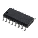
| 描述 | IC SWITCH QUAD CMOS 16SOIC |
| 产品分类 | |
| 品牌 | Vishay Siliconix |
| 数据手册 | |
| 产品图片 |
|
| 产品型号 | DG308BDY-T1-E3 |
| rohs | 无铅 / 符合限制有害物质指令(RoHS)规范要求 |
| 产品系列 | - |
| 供应商器件封装 | 16-SOIC N |
| 其它名称 | DG308BDY-T1-E3DKR |
| 功能 | |
| 包装 | Digi-Reel® |
| 安装类型 | 表面贴装 |
| 导通电阻 | 160 欧姆 |
| 封装/外壳 | 16-SOIC(0.154",3.90mm 宽) |
| 工作温度 | -40°C ~ 85°C |
| 标准包装 | 1 |
| 电压-电源,单/双 (±) | 12V, ±15V |
| 电压源 | 单/双电源 |
| 电流-电源 | 1µA |
| 电路 | 4 x SPST - NC |


PDF Datasheet 数据手册内容提取
CG2 / DG2 VISHAY Vishay Semiconductors Standard Sinterglass Diode Features • Specially designed for clamping circuits, horizon- tal deflection systems and damper applications (cid:127) High temperature metallurgically bonded con- struction (cid:127) Cavity-free glass passivated junction (cid:127) 2.0 ampere operation at T = 50°C with no ther- amb mal runaway (cid:127) Hermetically sealed package 17031 Mechanical Data Polarity: Color band denotes cathode end Case: DO-204AP Sintered glass case Mounting Position: Any Terminals: Solder plated axial leads, solderable per Weight: approx. 560 mg MILSTD- 750, Method 2026 Parts Table Part Type differentiation Package CG2 V = 1400 V DO-204AP(G-1) RRM DG2 V = 1500 V DO-204AP(G-1) RRM Absolute Maximum Ratings T = 25°C, unless otherwise specified amb Parameter Test condition Part Symbol Value Unit Reverse voltage = Repetitive see electrical characteristics CG2 V = V 1400 V R RRM peak reverse voltage DG2 V = V 1500 V R RRM Maximum average forward 0.375 " (9.5 mm) lead length at I 2.0 A F(AV) rectified current T = 50°C amb Peak forward surge current 8.3 ms single half sine wave I 40 A FSM superimposed on rated load (JEDEC Method) Maximum full load reverse 0.375 " (9.5 mm) lead length at I 200 µA R(AV) current full cycle average T =100°C amb Operating junction and storage T, T - 55 to + 175 °C J STG temperature range Maximum Thermal Resistance T = 25°C, unless otherwise specified amb Parameter Test condition Symbol Value Unit Typical thermal resistance 1) RθJA 55 K/W 1) Thermal resistance from junction to ambient at 0.375 " (9.5 mm) lead length, P.C.B. mounted Document Number 86082 www.vishay.com Rev. 1.3, 11-Aug-04 1
CG2 / DG2 VISHAY Vishay Semiconductors Electrical Characteristics T = 25°C, unless otherwise specified amb Parameter Test condition Part Symbol Min Typ. Max Unit Maximum instantaneous I = 2.0 A V 1.1 V F F forward voltage Maximum reverse current V = V , T = 25°C I 5.0 µA R RRM amb R V = V , T = 100°C I 100 µA R RRM amb R Maximum reverse recovery time I = 0.5 A, I = 50 mA CG2 t 15 µs F R rr DG2 t 20 µs rr I = 0.5 A, I = 1.0 A, I = 0.25 A CG2 t 1.0 1.5 µs F R r rr DG2 t 1.0 1.5 µs rr Typical junction capacitance V = 4.0 V, f = 1 MHz C 15 pF R j Typical Characteristics (T = 25 °C unless otherwise specified) amb A) 2.0 A) 10 ( Resistiveor ( Current 1.5 InductiveL0o.a3d75"(9.5mm) Current TJ=150°C Rectified 1.0 LeadILpekn/IgAtVh=π Forward 1 orward 0.5 CapacitanceLoad neous 0.1 TJ=25°C eF Ipk/IAV=51.00 nta PulseWidth=300µs ag 20 sta 1%DutyCycle ver 0 In0.01 A 0 25 50 75 100 125 150 175 0.4 0.6 0.8 1.0 1.2 1.4 1.6 gcg2_01 AmbientTemperature(°C) gcg2_03 InstantaneousForwardVoltage(V) Figure1. Forward Current Derating Curve Figure3. Typical Instantaneous Forward Characteristics 50 A) 10 A) 8.3msSingleHalfSine-Wave µ( nt( 40 (JEDECMethod) ent Curre TNJo=Lo2a5d°CCondition Curr 1 TJ=125°C e e 30 s urg ver S e R ward 20 TJ=TJmax. ous 0.1 or ne kF 10 nta a a Pe nst 0.01 TJ=25°C 0 I 1 10 100 0 20 40 60 80 100 gcg2_02 NumberofCyclesat60Hz gcg2_04 PercentofRatedPeakReverseVoltage(%) Figure2. Maximum Non-Repetitive Peak Forward Surge Current Figure4. Typical Reverse Characteristics www.vishay.com Document Number 86082 2 Rev. 1.3, 11-Aug-04
CG2 / DG2 VISHAY Vishay Semiconductors 30 TJ=25°C F) f=1.0MHz p Vsig=50mVp-p ( e nc 10 a cit a p a C n o cti n u J 1 1 10 100 gcg2_05 ReverseVoltage(V) Figure5. Typical Junction Capacitance Package Dimensions in mm (Inches) 0.86(0.034) 0.71(0.028) 25.4(1.0) DIA. MIN. 6.1(0.240) MAX. 3.8(0.150) 2.5(0.100) DIA. 25.4(1.0) MIN. 17030 Document Number 86082 www.vishay.com Rev. 1.3, 11-Aug-04 3
CG2 / DG2 VISHAY Vishay Semiconductors Ozone Depleting Substances Policy Statement It is the policy of Vishay Semiconductor GmbH to 1. Meet all present and future national and international statutory requirements. 2. Regularly and continuously improve the performance of our products, processes, distribution and operatingsystems with respect to their impact on the health and safety of our employees and the public, as well as their impact on the environment. It is particular concern to control or eliminate releases of those substances into the atmosphere which are known as ozone depleting substances (ODSs). The Montreal Protocol (1987) and its London Amendments (1990) intend to severely restrict the use of ODSs and forbid their use within the next ten years. Various national and international initiatives are pressing for an earlier ban on these substances. Vishay Semiconductor GmbH has been able to use its policy of continuous improvements to eliminate the use of ODSs listed in the following documents. 1. Annex A, B and list of transitional substances of the Montreal Protocol and the London Amendments respectively 2. Class I and II ozone depleting substances in the Clean Air Act Amendments of 1990 by the Environmental Protection Agency (EPA) in the USA 3. Council Decision 88/540/EEC and 91/690/EEC Annex A, B and C (transitional substances) respectively. Vishay Semiconductor GmbH can certify that our semiconductors are not manufactured with ozone depleting substances and do not contain such substances. We reserve the right to make changes to improve technical design and may do so without further notice. Parameters can vary in different applications. All operating parameters must be validated for each customer application by the customer. Should the buyer use Vishay Semiconductors products for any unintended or unauthorized application, the buyer shall indemnify Vishay Semiconductors against all claims, costs, damages, and expenses, arising out of, directly or indirectly, any claim of personal damage, injury or death associated with such unintended or unauthorized use. Vishay Semiconductor GmbH, P.O.B. 3535, D-74025 Heilbronn, Germany Telephone: 49 (0)7131 67 2831, Fax number: 49 (0)7131 67 2423 www.vishay.com Document Number 86082 4 Rev. 1.3, 11-Aug-04
Legal Disclaimer Notice Vishay Disclaimer All product specifications and data are subject to change without notice. Vishay Intertechnology, Inc., its affiliates, agents, and employees, and all persons acting on its or their behalf (collectively, “Vishay”), disclaim any and all liability for any errors, inaccuracies or incompleteness contained herein or in any other disclosure relating to any product. Vishay disclaims any and all liability arising out of the use or application of any product described herein or of any information provided herein to the maximum extent permitted by law. The product specifications do not expand or otherwise modify Vishay’s terms and conditions of purchase, including but not limited to the warranty expressed therein, which apply to these products. No license, express or implied, by estoppel or otherwise, to any intellectual property rights is granted by this document or by any conduct of Vishay. The products shown herein are not designed for use in medical, life-saving, or life-sustaining applications unless otherwise expressly indicated. Customers using or selling Vishay products not expressly indicated for use in such applications do so entirely at their own risk and agree to fully indemnify Vishay for any damages arising or resulting from such use or sale. Please contact authorized Vishay personnel to obtain written terms and conditions regarding products designed for such applications. Product names and markings noted herein may be trademarks of their respective owners. Document Number: 91000 www.vishay.com Revision: 18-Jul-08 1
Mouser Electronics Authorized Distributor Click to View Pricing, Inventory, Delivery & Lifecycle Information: V ishay: CG2-E3/54 DG308BDY-T1-E3 CG2/4 DG2/4