ICGOO在线商城 > 集成电路(IC) > 接口 - 模拟开关,多路复用器,多路分解器 > DG2706DN-T1-E4

 Datasheet下载
- 型号: DG2706DN-T1-E4
- 制造商: Vishay
- 库位|库存: xxxx|xxxx
- 要求:
| 数量阶梯 | 香港交货 | 国内含税 |
| +xxxx | $xxxx | ¥xxxx |
查看当月历史价格
查看今年历史价格
DG2706DN-T1-E4产品简介:
ICGOO电子元器件商城为您提供DG2706DN-T1-E4由Vishay设计生产,在icgoo商城现货销售,并且可以通过原厂、代理商等渠道进行代购。 DG2706DN-T1-E4价格参考。VishayDG2706DN-T1-E4封装/规格:接口 - 模拟开关,多路复用器,多路分解器, 4 Circuit IC Switch 2:1 5.5 Ohm 16-miniQFN (1.8x2.6)。您可以下载DG2706DN-T1-E4参考资料、Datasheet数据手册功能说明书,资料中有DG2706DN-T1-E4 详细功能的应用电路图电压和使用方法及教程。
| 参数 | 数值 |
| 产品目录 | 集成电路 (IC)半导体 |
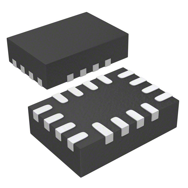
| 描述 | IC SWITCH QUAD SPDT 16-MINIQFN模拟开关 IC Quad SPDT Hi-Speed Low Voltage |
| 产品分类 | |
| 品牌 | Vishay SiliconixVishay / Siliconix |
| 产品手册 | |
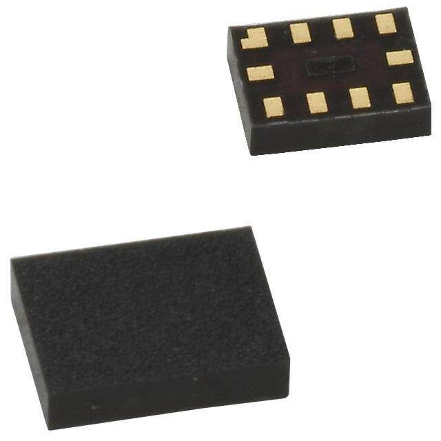
| 产品图片 |
|
| rohs | 符合RoHS无铅 / 符合限制有害物质指令(RoHS)规范要求 |
| 产品系列 | 开关 IC,模拟开关 IC,Vishay / Siliconix DG2706DN-T1-E4- |
| 数据手册 | |
| 产品型号 | DG2706DN-T1-E4DG2706DN-T1-E4 |
| 产品种类 | 模拟开关 IC |
| 供应商器件封装 | 16-迷你型QFN(1.8x2.6) |
| 其它名称 | DG2706DN-T1-E4CT |
| 功能 | |
| 包装 | 剪切带 (CT) |
| 商标 | Vishay / Siliconix |
| 安装类型 | 表面贴装 |
| 安装风格 | SMD/SMT |
| 导通电阻 | 5.5 欧姆 |
| 导通电阻—最大值 | 8 Ohms |
| 封装 | Reel |
| 封装/外壳 | 16-WFQFN |
| 封装/箱体 | miniQFN-16 |
| 工作温度 | -40°C ~ 85°C |
| 工作电源电压 | 3 V |
| 工厂包装数量 | 6000 |
| 开关数量 | 4 |
| 开关电流—最大值 | +/- 250 mA |
| 开关配置 | SPDT |
| 最大功率耗散 | 525 mW |
| 最大工作温度 | + 85 C |
| 最小工作温度 | - 40 C |
| 标准包装 | 1 |
| 电压-电源,单/双 (±) | 1.65 V ~ 4.3 V |
| 电压源 | 单电源 |
| 电流-电源 | 1µA |
| 电源电压-最大 | 4.3 V |
| 电源电压-最小 | 1.65 V |
| 电源电流—最大值 | 0.001 mA |
| 电路 | 4 x SPDT |
| 空闲时间—最大值 | 35 ns |
| 系列 | DG2706 |
| 运行时间—最大值 | 45 ns |
| 零件号别名 | DG2706DN-E4 |


PDF Datasheet 数据手册内容提取
DG2706 Vishay Siliconix High Speed, Low Voltage, 3 , Quad SPDT CMOS Analog Switch DESCRIPTION FEATURES The DG2706 is a high speed, low voltage, low • Operation voltage range: 1.65 V to 4.3 V On-resistance, quad SPDT (single pole double throw) (cid:129) Guaranteed On-resistance: 3.0 at 3.15 V analog switch. It operates from a 1.65 V to 4.3 V single (cid:129) Low voltage logic threshold power supply and achieves 3 switch On-resistance. When (cid:129) Low crosstalk: - 70 dB turned on, each switch conducts equally in both directions. (cid:129) High off-isolation: - 90 dB Its switch on resistance flatness is 0.6 and channel to (cid:129) Ultra small package: miniQFN16 of 1.8 mm x 2.6 mm channel matching is of 0.3 when powered with single 3.15 V supply. All channels guaranteed break before make APPLICATIONS switching. (cid:129) Dual SIM card switch Control logic input has 0.5 V to 1.65 V logic threshold. It features a 190 MHz - 3 dB bandwidth, - 90 dB crosstalk and (cid:129) A/V and analog signal routing - 70 dB off-isolation at 1 MHz. (cid:129) Battery operated devices The DG2706 is an ideal fit for low voltage battery powered (cid:129) Data acquisition systems devices switching audio, video, multi-media data streams, (cid:129) Communications systems and control signals between different functional circuits or (cid:129) Medical and ATE equipments ports. The DG2707 comes in a small miniQFN-16 lead package (1.8 mm x 2.6 mm x 0.75 mm). As a committed partner to community and the environment, Vishay Siliconix manufactures this product with the lead(Pb)-free device terminations and is 100 % RoHS compliant. FUNCTIONAL BLOCK DIAGRAM AND PIN CONFIGURATION miniQFN-16L NO4 GND IN1 NC3 12 11 10 9 COM4 13 8 COM3 NC4 14 7 NO3 VXX NO1 15 6 NC2 COM1 16 5 COM2 1 2 3 4 Pin 1: LONG LEAD C1 V+ N2 O2 N I N Top View Device Marking: VXX Traceability Code: V is DG2706DN XX = Date/Lot ORDERING INFORMATION Temp. Range Package Part Number - 40 °C to 85 °C miniQFN-16 DG2706DN-T1-E4 Document Number: 68392 www.vishay.com S11-0176-Rev. B, 07-Feb-11 1
DG2706 Vishay Siliconix TRUTH TABLE DG2706 QUAD SPDT, miniQFN-16L Select Input On Switches IN1 (Pin 10) IN2 (Pin 3) Description (Pin) Common (Pin) 0 X NC1 (Pin 1) COM1 (Pin 16) 1 X NO1 (Pin 15) 0 X NC4 (Pin 14) COM4 (Pin 13) 1 X NO4 (Pin 12) 0 NC2 (Pin 6) X COM2 (Pin 5) 1 NO2 (Pin 4) 0 NC3 (Pin 9) X COM3 (Pin 3) 1 NO3 (Pin 7) ABSOLUTE MAXIMUM RATINGS (T = 25 °C, unless otherwise noted) A Parameter Limit Unit V+ - 0.3 to 5.0 Reference to GND V IN, COM, NC, NOa - 0.3 to (V+ + 0.3) Current (Any terminal except NO, NC or COM) 30 Continuous Current (NO, NC, or COM) ± 250 mA Peak Current (Pulsed at 1 ms, 10 % Duty Cycle) ± 500 Storage Temperature (D Suffix) - 65 to 150 °C Thermal Resistance (Package)b miniQFN-16 152 °C/W Power Dissipation (Package)b miniQFN-16c, d 525 mW Notes: a.Signals on NC, NO, or COM or IN exceeding V+ will be clamped by internal diodes. Limit forward diode current to maximum current ratings. b.All leads welded or soldered to PC board. c. Derate 6.6 mW/°C above 70 °C d.Manual soldering with iron is not recommended for leadless components. The miniQFN-16 is a leadless package. The end of the lead terminal is exposed copper (not plated) as a result of the singulation process in manufacturing. A solder fillet at the exposed copper lip cannot be guaranteed and is not required to ensure adequate bottom side solder interconnection. www.vishay.com Document Number: 68392 2 S11-0176-Rev. B, 07-Feb-11
DG2706 Vishay Siliconix SPECIFICATIONS (V+ = 3.15 V) Limits - 40 °C to 85 °C Test Conditions Parameter Symbol Otherwise Unless Specified Temp.b Min.d Typ.c Max.d Unit Analog Switch Analog Signal Rangee V R Full 0 V+ V ANALOG DS(on) Room 3 5.5 On-Resistance R V+ = 3.15 V, I = 10 mA, V = 1.0 V DS(on) NO/NC COM Full 6 R Match R V+ = 3.15 V, I = 10 mA, V = 1.0 V Room 0.3 ON (ON) NO/NC COM RON Resistance Flatness RON V+ = 3.15 V, INO/NC = 10 mA, Room 0.6 Room - 5 5 I NO/NC(off) Channel Off Leakage V+ = 3.6 V, V = 0.5 V/3 V, Full - 10 10 NO/NC Current VCOM = 3 V/0.5 V Room - 5 5 I nA COM(off) Full - 10 10 Channel-On Leakage Room - 10 10 I V+ = 3.6 V, V , V = 3 V/0.5 V Current COM(on) NO/NC COM Full - 20 20 Digital Control Input High Voltage V Full 1.65 INH V Input Low Voltage V Full 0.4 INL Input Current I or I V = 0 or V+ Full - 1 1 µA INL INH IN Dynamic Characteristics Room 1 Break-Before-Make Time t BBM Full 5 Room 20 45 Enable Turn-On Time t V , V = 1.5 V, R = 50 , C = 35 pF ns ON(EN) NO NC L L Full 55 Room 15 35 Enable Turn-Off Time t OFF(EN) Full 45 Charge Injectiond Q C = 1 nF, R = 0 , V = 2 V Room 3 pC INJ L GEN NC/NO Off-Isolationd OIRR Room - 70 V+ = 3.15 V, f = 1 MHz, R = 50 , C = 5 pF dB Crosstalkd, f X L L Room - 90 TALK Bandwidthd BW V+ = 3.15 V, R = 50 , C = 5 pF, - 3 dB Room 190 MHz L L Total Harmonic Distortiond THD V+ = 3.15 V, R = 600 Room 0.02 % LOAD CS 16 N , N Off Capacitanced NC(off) O C CS V+ = 3.15 V, f = 1 MHz Room 15 pF NO(on) Channel-On Capacitanced C 31 COM(on) Power Supply Power Supply Range V+ 1.65 4.3 V Power Supply Current I+ V = 0 or V+ Full 1 µA IN Notes: a. Room = 25 °C, Full = as determined by the operating suffix. b. The algebraic convention whereby the most negative value is a minimum and the most positive a maximum, is used in this data sheet. c. Typical values are for design aid only, not guaranteed nor subject to production testing. d. Guarantee by design, not subjected to production test. e. V = input voltage to perform proper function. IN f. Crosstalk measured between channels. Stresses beyond those listed under “Absolute Maximum Ratings” may cause permanent damage to the device. These are stress ratings only, and functional operation of the device at these or any other conditions beyond those indicated in the operational sections of the specifications is not implied. Exposure to absolute maximum rating conditions for extended periods may affect device reliability. Document Number: 68392 www.vishay.com S11-0176-Rev. B, 07-Feb-11 3
DG2706 Vishay Siliconix TYPICAL CHARACTERISTICS (T = 25°C, unless otherwise noted) A 26 40 24 T = 25 °C ION = 10 mA 35 22 COM V+ = 1.65 V, ION = 10 mA ΩResistance () 11124680 V+ = 1.65 V ΩResistance () 223050 + +8 52 5°C °C On- 12 On- - 40 °C - N 10 - N 15 O O R 8 R 10 6 V+ = 3.15 V V+ = 3.6 V 5 4 2 0 0 0.5 1.0 1.5 2.0 2.5 3.0 3.5 4.0 0 0.5 1.0 1.5 2.0 VD - Analog Voltage (V) VD - Analog Voltage (V) R vs. V and Single Supply Voltage R vs. Analog Voltage and Temperature ON D ON 5 10 DG2706 V+ = 3.15 V, ION = 10 mA RL = 600 Ω VSignal = 1 VRMS 4 1 Ω) e ( + 85 °C c V+ = 1.65 V n sta + 25 °C %) esi 3 D ( 0.1 R H On- - 40 °C T V+ = 3.15 V - N O R 2 0.01 V+ = 3.6 V 1 0 0 0.5 1.0 1.5 2.0 2.5 3.0 3.5 4.0 10 100 1000 10000 100000 VD - Analog Voltage (V) Frequency (Hz) R vs. Analog Voltage and Temperature Switching Threshold vs. Supply Voltage ON 5 10 mA V+ = 3.6 V, ION = 10 mA 1 mA Ωstance () 4 + 85 °C urrent (A) 11000 µµAA R - On-ResiON 23 - 40 °C + 25 °C I+ - Supply C 110100 µnnAAA VV++ == 33..165 V V V+ = 1.65 V 1 nA 1 100 pA 0 0.5 1.0 1.5 2.0 2.5 3.0 3.5 4.0 10 100 1K 10K 100K 1M 10M VD - Analog Voltage (V) Input Switching Frequency (Hz) R vs. Analog Voltage and Temperature Supply Current vs. Input Switching Frequency ON www.vishay.com Document Number: 68392 4 S11-0176-Rev. B, 07-Feb-11
DG2706 Vishay Siliconix TYPICAL CHARACTERISTICS (T = 25°C, unless otherwise noted) A 1000 10 V+ = 3.15 V Loss 0 - 10 V+ = 3.15 V eakage Currrent (pA) 11000 ICOM(on) INO/NC(off) (dB)s, OIRR, X TALK ----- 6543200000 RL = 50 Ω OIRR XTALK L s o - 70 L ICOM(off) - 80 - 90 1 - 100 - 60 - 40 - 20 0 20 40 60 80 100 120 140 100K 1M 10M 100M 1G Temperature (°C) Frequency (Hz) Leakage Current vs. Temperature Insertion Loss, Off-Isolation Crosstalk vs. Frequency 1.5 1.4 1.3 V) d ( 1.2 ol sh 1.1 e hr T 1.0 g n hi 0.9 c wit S 0.8 - T V 0.7 0.6 0.5 1.0 1.5 2.0 2.5 3.0 3.5 4.0 4.5 5.0 V+ - Supply Voltage (V) Switching Threshold vs. Supply Voltage Document Number: 68392 www.vishay.com S11-0176-Rev. B, 07-Feb-11 5
DG2706 Vishay Siliconix TEST CIRCUITS V+ LInopguict VINH 50 % ttrf << 55 nnss V+ VINL Switch Output Switch NO or NC COM Input VOUT Logic 0.9 x VOUT IN Switch Input RL CL Output GND 50 Ω 35 pF 0 V tON tOFF 0 V Logic "1" = Switch on CL (includes fixture and stray capacitance) Logic input waveforms inverted for switches that have the opposite logic sense. VOUT = VCOM(R +RLR ) L ON Figure 1. Switching Time V+ Logic VINH tr < 5 ns V+ Input tf < 5 ns NO COM VINL VNO VO NC VNC RL CL 50 Ω 35 pF VNC = VNO IN VO 90 % GND Switch 0 V Output tD tD CL (includes fixture and stray capacitance) Figure 2. Break-Before-Make Interval V+ Rgen NC or NO V+ COM VOUT ΔVOUT VOUT + IN IN CL = 1 nF On On Vgen VIN = 0 - V+ Off GND Q = ΔVOUT x CL IN depends on switch configuration: input polarity determined by sense of switch. Figure 3. Charge Injection www.vishay.com Document Number: 68392 6 S11-0176-Rev. B, 07-Feb-11
DG2706 Vishay Siliconix TEST CIRCUITS V+ V+ 10 nF 10 nF V+ NC or NO V+ 0 V, 2.4 V COM IN Meter COM COM IN HP4192A 0 V, 2.4 V Impedance Analyzer RL GND NC or NO or Equivalent GND f = 1 MHz Analyzer V COM OffIsolation = 20log V NO /NC Figure 4. Off-Isolation Figure 5. Channel Off/On Capacitance Vishay Siliconix maintains worldwide manufacturing capability. Products may be manufactured at one of several qualified locations. Reliability data for Silicon Technology and Package Reliability represent a composite of all qualified locations. For related documents such as package/tape drawings, part marking, and reliability data, see www.vishay.com/ppg?68392. Document Number: 68392 www.vishay.com S11-0176-Rev. B, 07-Feb-11 7
Package Information www.vishay.com Vishay Siliconix Thin miniQFN16 Case Outline A D B Terminal tip 1(46) x b 00..1005MM CCAB 12 11 10 9 9 10 11 12 13 8 8 13 C 14 7 7 14 E 10 15 6 6 15 0. 16 5 5 16 L1 1 2 3 4 4 3 2 1 Pin #1 identifier (5) 15 x L e 0.10C Top view Bottom view 0.10C C A 0.10C Seating plane A3 Side view MILLIMETERS (1) INCHES DIMENSIONS MIN. NOM. MAX. MIN. NOM. MAX. A 0.50 0.55 0.60 0.020 0.022 0.024 A1 0 - 0.05 0 - 0.002 A3 0.15 ref. 0.006 ref. b 0.15 0.20 0.25 0.006 0.008 0.010 D 2.50 2.60 2.70 0.098 0.102 0.106 e 0.40 BSC 0.016 BSC E 1.70 1.80 1.90 0.067 0.071 0.075 L 0.35 0.40 0.45 0.014 0.016 0.018 L1 0.45 0.50 0.55 0.018 0.020 0.022 N (3) 16 16 Nd (3) 4 4 Ne (3) 4 4 Notes (1) Use millimeters as the primary measurement. (2) Dimensioning and tolerances conform to ASME Y14.5M. - 1994. (3) N is the number of terminals. Nd and Ne is the number of terminals in each D and E site respectively. (4) Dimensions b applies to plated terminal and is measured between 0.15 mm and 0.30 mm from terminal tip. (5) The pin 1 identifier must be existed on the top surface of the package by using identification mark or other feature of package body. (6) Package warpage max. 0.05 mm. ECN: T16-0226-Rev. B, 09-May-16 DWG: 6023 Revision: 09-May-16 1 Document Number: 64694 For technical questions, contact: analogswitchtechsupport@vishay.com THIS DOCUMENT IS SUBJECT TO CHANGE WITHOUT NOTICE. THE PRODUCTS DESCRIBED HEREIN AND THIS DOCUMENT ARE SUBJECT TO SPECIFIC DISCLAIMERS, SET FORTH AT www.vishay.com/doc?91000
PAD Pattern Vishay Siliconix RECOMMENDED MINIMUM PADS FOR MINI QFN 16L 0.562 (0.0221) 0.400 (0.0157) 1 0.225 (0.0089) 2.900 (0.1142) 0.463 (0.0182) 1.200 (0.0472) 2.100 (0.0827) Mounting Footprint Dimensions in mm (inch) Document Number: 66557 www.vishay.com Revision: 05-Mar-10 1
Legal Disclaimer Notice www.vishay.com Vishay Disclaimer ALL PRODUCT, PRODUCT SPECIFICATIONS AND DATA ARE SUBJECT TO CHANGE WITHOUT NOTICE TO IMPROV E RELIABILITY, FUNCTION OR DESIGN OR OTHERWISE. Vishay Intertechnology, Inc., its affiliates, agents, and employees, and all persons acting on its or their behalf (collectively, “Vishay”), disclaim any and all liability for any errors, inaccuracies or incompleteness contained in any datasheet or in any other disclosure relating to any product. Vishay makes no warranty, representation or guarantee regarding the suitability of the products for any particular purpose o r the continuing production of any product. To the maximum extent permitted by applicable law, Vishay disclaims (i) any and all liability arising out of the application or use of any product, (ii) any and all liability, including without limitation special, consequential or incidental damages, and (iii) any and all implied warranties, including warranties of fitness for particular purpose, non-infringement and merchantability. Statements regarding the suitability of products for certain types of applications are based on Vishay’s knowledge of typical requirements that are often placed on Vishay products in generic applications. Such statements are not binding statements about the suitability of products for a particular application. It is the customer’s responsibility to validate that a particular product with the properties described in the product specification is suitable for use in a particular application. Parameters provided in datasheets and / or specifications may vary in different applications and performance may vary over time. All operating parameters, including typical parameters, must be validated for each customer application by the customer’s technical experts. Product specifications do not expand or otherwise modify Vishay’s terms and conditions of purchase, including but not limited to the warranty expressed therein. Except as expressly indicated in writing, Vishay products are not designed for use in medical, life-saving, or life-sustainin g applications or for any other application in which the failure of the Vishay product could result in personal injury or death. Customers using or selling Vishay products not expressly indicated for use in such applications do so at their own risk . Please contact authorized Vishay personnel to obtain written terms and conditions regarding products designed for such applications. No license, express or implied, by estoppel or otherwise, to any intellectual property rights is granted by this documen t or by any conduct of Vishay. Product names and markings noted herein may be trademarks of their respective owners. © 2019 VISHAY INTERTECHNOLOGY, INC. ALL RIGHTS RESERVED Revision: 01-Jan-2019 1 Document Number: 91000