 Datasheet下载
- 型号: DF6A6.8FUT1G
- 制造商: ON Semiconductor
- 库位|库存: xxxx|xxxx
- 要求:
| 数量阶梯 | 香港交货 | 国内含税 |
| +xxxx | $xxxx | ¥xxxx |
查看当月历史价格
查看今年历史价格
DF6A6.8FUT1G产品简介:
ICGOO电子元器件商城为您提供DF6A6.8FUT1G由ON Semiconductor设计生产,在icgoo商城现货销售,并且可以通过原厂、代理商等渠道进行代购。 DF6A6.8FUT1G价格参考。ON SemiconductorDF6A6.8FUT1G封装/规格:TVS - 二极管, 。您可以下载DF6A6.8FUT1G参考资料、Datasheet数据手册功能说明书,资料中有DF6A6.8FUT1G 详细功能的应用电路图电压和使用方法及教程。
| 参数 | 数值 |
| 产品目录 | |
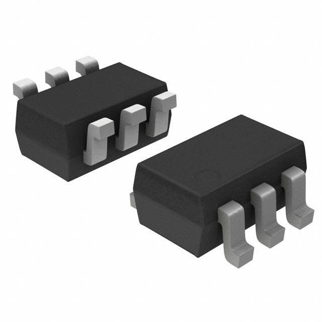
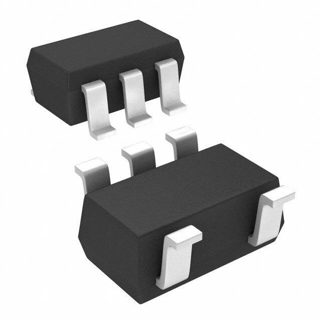
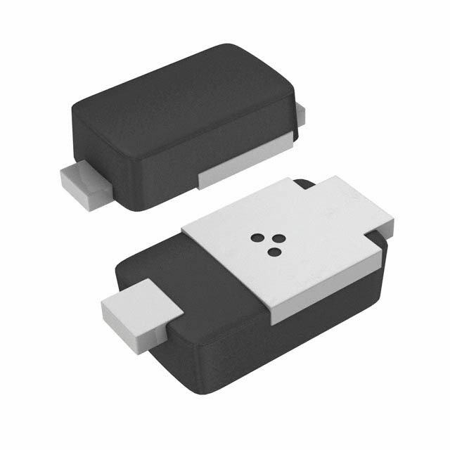
| 描述 | TVS DIODE 5VWM SC886TVS二极管阵列 6.4V 75W TVS Quad Array |
| 产品分类 | |
| 品牌 | ON Semiconductor |
| 产品手册 | |
| 产品图片 |
|
| rohs | 符合RoHS无铅 / 符合限制有害物质指令(RoHS)规范要求 |
| 产品系列 | 二极管与整流器,TVS二极管,TVS二极管阵列,ON Semiconductor DF6A6.8FUT1G- |
| 数据手册 | |
| 产品型号 | DF6A6.8FUT1G |
| PCN设计/规格 | |
| 不同频率时的电容 | 40pF @ 1MHz |
| 产品种类 | TVS二极管阵列 |
| 供应商器件封装 | SC-88/SC70-6/SOT-363 |
| 其它名称 | DF6A6.8FUT1GOSDKR |
| 击穿电压 | 6.4 V |
| 功率-峰值脉冲 | 75W |
| 包装 | Digi-Reel® |
| 单向通道 | 4 |
| 双向通道 | - |
| 商标 | ON Semiconductor |
| 安装类型 | 表面贴装 |
| 安装风格 | SMD/SMT |
| 封装 | Reel |
| 封装/外壳 | 6-TSSOP,SC-88,SOT-363 |
| 封装/箱体 | SC-70-6 |
| 尺寸 | 1.25 mm W x 2 mm L |
| 峰值脉冲功率耗散 | 75 W |
| 工作温度 | -55°C ~ 150°C |
| 工作电压 | 5 V |
| 工厂包装数量 | 3000 |
| 应用 | 通用 |
| 最大工作温度 | + 150 C |
| 最小工作温度 | - 55 C |
| 极性 | Unidirectional |
| 标准包装 | 1 |
| 电压-击穿(最小值) | 6.4V |
| 电压-反向关态(典型值) | 5V |
| 电压-箝位(最大值)@Ipp | - |
| 电流-峰值脉冲(10/1000µs) | - |
| 电源线路保护 | 无 |
| 端接类型 | SMD/SMT |
| 类型 | 齐纳 |
| 系列 | DF6A6.8FUT1 |
| 通道 | 4 Channels |


- 商务部:美国ITC正式对集成电路等产品启动337调查
- 曝三星4nm工艺存在良率问题 高通将骁龙8 Gen1或转产台积电
- 太阳诱电将投资9.5亿元在常州建新厂生产MLCC 预计2023年完工
- 英特尔发布欧洲新工厂建设计划 深化IDM 2.0 战略
- 台积电先进制程称霸业界 有大客户加持明年业绩稳了
- 达到5530亿美元!SIA预计今年全球半导体销售额将创下新高
- 英特尔拟将自动驾驶子公司Mobileye上市 估值或超500亿美元
- 三星加码芯片和SET,合并消费电子和移动部门,撤换高东真等 CEO
- 三星电子宣布重大人事变动 还合并消费电子和移动部门
- 海关总署:前11个月进口集成电路产品价值2.52万亿元 增长14.8%


PDF Datasheet 数据手册内容提取
DF6A6.8FUT Quad Array for ESD Protection This quad voltage suppressor is designed for applications requiring transient overvoltage protection capability. It is intended for use in voltage and ESD sensitive equipment such as computers, printers, business machines, communication systems, medical equipment, and http://onsemi.com other applications. Its quad junction common anode design protects four separate lines using only one package. These devices are ideal for situations where board space is at a premium. 1 6 Specification Features • 2 5 SC−88 Package Allows Four Separate Unidirectional Configurations • Low Leakage < 1 (cid:2)A @ 5 Volt 3 4 • Breakdown Voltage: 6.4 − 7.2 Volt @ 5 mA • Low Capacitance (40 pF typical) • ESD Protection Meeting 61000−4−2 Level 4 and 16 kV Human Body Model MARKING • DIAGRAM These are Pb−Free Devices Mechanical Characteristics 1 6 • Void Free, Transfer−Molded, Thermosetting Plastic Case SC−88 • Corrosion Resistant Finish, Easily Solderable CASE 419B−02 68(cid:2) M(cid:2) • Package Designed for Optimal Automated Board Assembly 1 • Small Package Size for High Density Applications 68 = Specific Device Code M = Date Code MAXIMUM RATINGS (TA = 25°C unless otherwise noted) (cid:2) = Pb−Free Package (Note: Microdot may be in either location.) Rating Symbol Value Unit Peak Power Dissipation @ 8 x 20 (cid:2)s Ppk 75 Watts ORDERING INFORMATION (Note 1) Steady State Power Dissipation PD 385 mW Device Package Shipping† (Note 2) DF6A6.8FUT1G SC−88 3000/Tape & Reel Thermal Resistance − R(cid:3)JA (Pb−Free) Junction−to−Ambient 328 °C/W DF6A6.8FUT2G SC−88 3000/Tape & Reel Derate Above 25°C 3.0 mW/°C (Pb−Free) Maximum Junction Temperature TJmax 150 °C †For information on tape and reel specifications, Operating Junction and Storage TJ, Tstg −55 to °C including part orientation and tape sizes, please Temperature Range +150 refer to our Tape and Reel Packaging Specifications Brochure, BRD8011/D. ESD Discharge VPP kV MIL STD 883C − Method 3015−6 16 IEC61000−4−2, Air Discharge 16 IEC61000−4−2, Contact Discharge 8 Lead Solder Temperature TL 260 °C (10 seconds duration) Stresses exceeding Maximum Ratings may damage the device. Maximum Ratings are stress ratings only. Functional operation above the Recommended Operating Conditions is not implied. Extended exposure to stresses above the Recommended Operating Conditions may affect device reliability. 1. Per Waveform Figure 1 2. Mounted on FR−5 Board = 1.0 X 0.75 X 0.062 in. © Semiconductor Components Industries, LLC, 2012 1 Publication Order Number: October, 2012 − Rev. 2 DF6A6.8FUT1/D
DF6A6.8FUT I IF VBRVRWM V IR VF IT V−I Curve ELECTRICAL CHARACTERISTICS Typical Max Max Breakdown Voltage Leakage Current Capacitance Max ZZ @ ZZK @ VBR @ 5 mA (Volts) IRM @ VRWM = 5 V @ 0 V Bias VF @ IF = 10 mA 5 mA 0.5 mA Device Device Marking Min Nom Max ((cid:2)A) (pF) (V) ((cid:3)) ((cid:3)) DF6A6.8FUT1G 68 6.4 6.8 7.2 1.0 40 1.25 30 300 DF6A6.8FUT2G 68 6.4 6.8 7.2 1.0 40 1.25 30 300 100 50 tr PEAK VALUE IRSM @ 8 (cid:2)s 90 ENT 80 PULSE WIDTH (tP) IS DEFINED pF) 45 E CURR 7600 APESA TKH ACTU RPOREINNTT W DHEECRAYE =T H8E (cid:2)s TANCE (ENCY 4305 ULS 50 HALF VALUE IRSM/2 @ 20 (cid:2)s PACIEQU 30 P AR AK 40 L Cz F 25 E 30 AH OF P 20 tP YPIC1 M 20 % T 15 10 0 10 0 20 40 60 80 0 1 2 3 4 5 t, TIME ((cid:2)s) BIAS VOLTAGE (VOLTS) Figure 1. 8 × 20 (cid:2)s Pulse Waveform Figure 2. Capacitance 1 10 S) P M A) A NT ( 0.1 NT ( E E R R R R 8 x 20 (cid:2)s per Figure 1 U U C C D 0.01 E R S A L W U FOR0.001 AK P , F PE I , p p 0.0001 I 1 0.6 0.7 0.8 0.9 1.0 1.1 1.2 8 9 10 11 12 VF, FORWARD VOLTAGE (VOLTS) VC, CLAMPING VOLTAGE (VOLTS) Figure 3. Forward Voltage Figure 4. Clamping Voltage versus Peak Pulse Current http://onsemi.com 2
DF6A6.8FUT PACKAGE DIMENSIONS SC−88/SC70−6/SOT−363 CASE 419B−02 ISSUE W D e NOTES: 1. DIMENSIONING AND TOLERANCING PER ANSI Y14.5M, 1982. 2. CONTROLLING DIMENSION: INCH. 3. 419B−01 OBSOLETE, NEW STANDARD 419B−02. 6 5 4 MILLIMETERS INCHES HE −E− DAIM 0M.8IN0 N0O.9M5 M1.A10X 0.M03IN1 0N.0O3M7 0M.0A43X A1 0.00 0.05 0.10 0.000 0.002 0.004 1 2 3 A3 0.20 REF 0.008 REF b 0.10 0.21 0.30 0.004 0.008 0.012 C 0.10 0.14 0.25 0.004 0.005 0.010 D 1.80 2.00 2.20 0.070 0.078 0.086 b6 PL E 1.15 1.25 1.35 0.045 0.049 0.053 0.2 (0.008) M E M e 0.65 BSC 0.026 BSC L 0.10 0.20 0.30 0.004 0.008 0.012 HE 2.00 2.10 2.20 0.078 0.082 0.086 A3 A C A1 L SOLDERING FOOTPRINT* 0.50 0.0197 0.65 0.025 0.65 0.025 0.40 0.0157 1.9 0.0748 (cid:2) mm (cid:3) SCALE 20:1 inches *For additional information on our Pb−Free strategy and soldering details, please download the ON Semiconductor Soldering and Mounting Techniques Reference Manual, SOLDERRM/D. ON Semiconductor and are registered trademarks of Semiconductor Components Industries, LLC (SCILLC). SCILLC owns the rights to a number of patents, trademarks, copyrights, trade secrets, and other intellectual property. A listing of SCILLC’s product/patent coverage may be accessed at www.onsemi.com/site/pdf/Patent−Marking.pdf. SCILLC reserves the right to make changes without further notice to any products herein. SCILLC makes no warranty, representation or guarantee regarding the suitability of its products for any particular purpose, nor does SCILLC assume any liability arising out of the application or use of any product or circuit, and specifically disclaims any and all liability, including without limitation special, consequential or incidental damages. “Typical” parameters which may be provided in SCILLC data sheets and/or specifications can and do vary in different applications and actual performance may vary over time. All operating parameters, including “Typicals” must be validated for each customer application by customer’s technical experts. SCILLC does not convey any license under its patent rights nor the rights of others. SCILLC products are not designed, intended, or authorized for use as components in systems intended for surgical implant into the body, or other applications intended to support or sustain life, or for any other application in which the failure of the SCILLC product could create a situation where personal injury or death may occur. Should Buyer purchase or use SCILLC products for any such unintended or unauthorized application, Buyer shall indemnify and hold SCILLC and its officers, employees, subsidiaries, affiliates, and distributors harmless against all claims, costs, damages, and expenses, and reasonable attorney fees arising out of, directly or indirectly, any claim of personal injury or death associated with such unintended or unauthorized use, even if such claim alleges that SCILLC was negligent regarding the design or manufacture of the part. SCILLC is an Equal Opportunity/Affirmative Action Employer. This literature is subject to all applicable copyright laws and is not for resale in any manner. PUBLICATION ORDERING INFORMATION LITERATURE FULFILLMENT: N. American Technical Support: 800−282−9855 Toll Free ON Semiconductor Website: www.onsemi.com Literature Distribution Center for ON Semiconductor USA/Canada P.O. Box 5163, Denver, Colorado 80217 USA Europe, Middle East and Africa Technical Support: Order Literature: http://www.onsemi.com/orderlit Phone: 303−675−2175 or 800−344−3860 Toll Free USA/Canada Phone: 421 33 790 2910 Fax: 303−675−2176 or 800−344−3867 Toll Free USA/Canada Japan Customer Focus Center For additional information, please contact your local Email: orderlit@onsemi.com Phone: 81−3−5817−1050 Sales Representative http://onsemi.com DF6A6_8FUT1/D 3
Mouser Electronics Authorized Distributor Click to View Pricing, Inventory, Delivery & Lifecycle Information: O N Semiconductor: DF6A6.8FUT1 DF6A6.8FUT1G DF6A6.8FUT2G SZDF6A6.8FUT1G