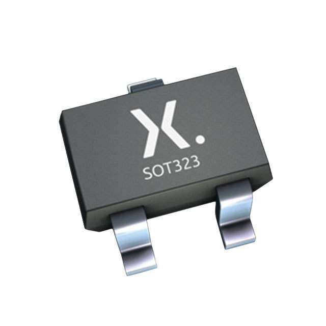
ICGOO在线商城 > DF2B6.8M1ACT(TPL3)
- 型号: DF2B6.8M1ACT(TPL3)
- 制造商: Toshiba America Electronic Components, Inc.
- 库位|库存: xxxx|xxxx
- 要求:
| 数量阶梯 | 香港交货 | 国内含税 |
| +xxxx | $xxxx | ¥xxxx |
查看当月历史价格
查看今年历史价格
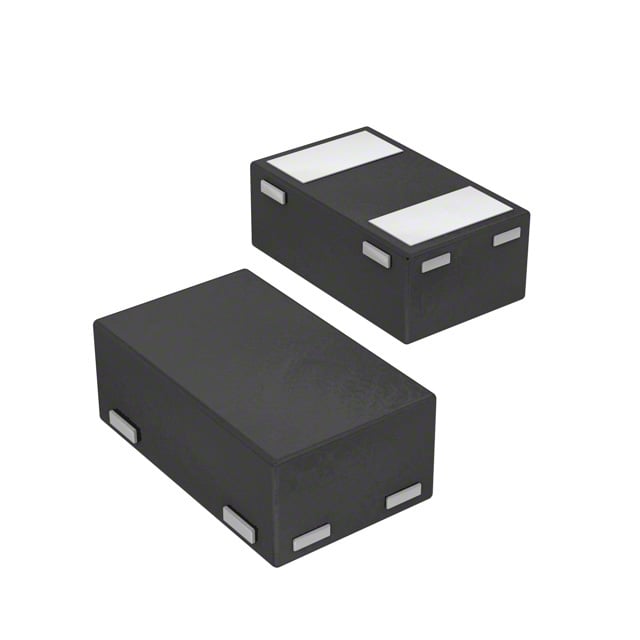
DF2B6.8M1ACT(TPL3)产品简介:
ICGOO电子元器件商城为您提供DF2B6.8M1ACT(TPL3)由Toshiba America Electronic Components, Inc.设计生产,在icgoo商城现货销售,并且可以通过原厂、代理商等渠道进行代购。 提供DF2B6.8M1ACT(TPL3)价格参考以及Toshiba America Electronic Components, Inc.DF2B6.8M1ACT(TPL3)封装/规格参数等产品信息。 你可以下载DF2B6.8M1ACT(TPL3)参考资料、Datasheet数据手册功能说明书, 资料中有DF2B6.8M1ACT(TPL3)详细功能的应用电路图电压和使用方法及教程。
| 参数 | 数值 |
| 产品目录 | |
| 描述 | TVS DIODE 5VWM 12VC CST2ESD 抑制器 ESD Diode 6V BI 0.3pF 0.5 IR 1 LN |
| 产品分类 | |
| 品牌 | ToshibaToshiba Semiconductor and Storage |
| 产品手册 | http://www.semicon.toshiba.co.jp/info/docget.jsp?type=datasheet&lang=en&pid=DF2B6.8M1ACT |
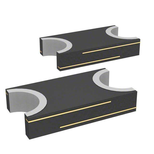
| 产品图片 |
|
| rohs | 符合RoHS无铅 / 符合限制有害物质指令(RoHS)规范要求 |
| 产品系列 | Toshiba DF2B6.8M1ACT(TPL3)- |
| 数据手册 | http://www.semicon.toshiba.co.jp/info/docget.jsp?type=datasheet&lang=en&pid=DF2B6.8M1ACT |
| 产品型号 | DF2B6.8M1ACT(TPL3)DF2B6.8M1ACT(TPL3) |
| 不同频率时的电容 | 0.3pF @ 1MHz |
| 产品培训模块 | http://www.digikey.cn/PTM/IndividualPTM.page?site=cn&lang=zhs&ptm=30275 |
| 产品种类 | ESD 抑制器 |
| 供应商器件封装 | CST2 |
| 其它名称 | DF2B6.8M1ACT(TPL3)DKR |
| 击穿电压 | 6 V |
| 功率-峰值脉冲 | - |
| 包装 | Digi-Reel® |
| 单向通道 | - |
| 双向通道 | 1 |
| 商标 | Toshiba |
| 安装类型 | 表面贴装 |
| 封装 | Reel |
| 封装/外壳 | SOD-882 |
| 封装/箱体 | SOD-882 |
| 工作温度 | - |
| 工厂包装数量 | 10000 |
| 应用 | 通用 |
| 标准包装 | 1 |
| 特色产品 | http://www.digikey.cn/product-highlights/zh/esd-protection-diodes/52610 |
| 电压-击穿(最小值) | 6V |
| 电压-反向关态(典型值) | 5V(最小值) |
| 电压-箝位(最大值)@Ipp | 12V (标准) |
| 电容 | 0.5 pF |
| 电流-峰值脉冲(10/1000µs) | 1A (8/20µs) |
| 电源线路保护 | 无 |
| 端接类型 | SMD/SMT |
| 类型 | 转向装置(轨至轨) |



- 商务部:美国ITC正式对集成电路等产品启动337调查
- 曝三星4nm工艺存在良率问题 高通将骁龙8 Gen1或转产台积电
- 太阳诱电将投资9.5亿元在常州建新厂生产MLCC 预计2023年完工
- 英特尔发布欧洲新工厂建设计划 深化IDM 2.0 战略
- 台积电先进制程称霸业界 有大客户加持明年业绩稳了
- 达到5530亿美元!SIA预计今年全球半导体销售额将创下新高
- 英特尔拟将自动驾驶子公司Mobileye上市 估值或超500亿美元
- 三星加码芯片和SET,合并消费电子和移动部门,撤换高东真等 CEO
- 三星电子宣布重大人事变动 还合并消费电子和移动部门
- 海关总署:前11个月进口集成电路产品价值2.52万亿元 增长14.8%


PDF Datasheet 数据手册内容提取
DF2B6.8M1ACT ESD Protection Diodes Silicon Epitaxial Planar DDDDFFFF2222BBBB6666....8888MMMM1111AAAACCCCTTTT 1111.... GGGGeeeennnneeeerrrraaaallll The DF2B6.8M1ACT is a TVS diode (ESD protection diode) protects semiconductor devices used in mobile device interfaces and other applications to protect against static electricity and noise. The DF2B6.8M1ACT provide to protect the latter part well by the low dynamic resistance. Furthermore, it is optimum the high speed signal application for the low capacitance performance. The DF2B6.8M1ACT is housed in an ultra-compact package (1.0 mm × 0.6 mm) to meet applications that require a small footprint. 2222.... AAAApppppppplllliiiiccccaaaattttiiiioooonnnnssss Mobile Equipment Smartphones Tablets Notebook PCs Desktop PCs Note: This product is designed for protection against electrostatic discharge (ESD) and is not intended for any other purpose, including, but not limited to, voltage regulation. 3333.... FFFFeeeeaaaattttuuuurrrreeeessss (1) Suitable for use with a 5.0 V signal line. (VRWM ≤ 5.0 V) (2) Protects devices with its high ESD performance. (VESD = ±12 kV (Contact), VESD = ±15 kV (Air) @IEC61000-4-2) (3) Low dynamic resistance protects semiconductor devices from static electricity and noise. (RDYN = 0.8 Ω (typ.)) (4) Compact package is suitable for use in high density board layouts such as in mobile devices. (1.0 mm × 0.6 mm size (Nickname: CST2)) 4444.... PPPPaaaacccckkkkaaaaggggiiiinnnngggg CST2 Start of commercial production 2012-02 ©2017-2018 1 2018-02-02 Toshiba Electronic Devices & Storage Corporation Rev.11.0
DF2B6.8M1ACT 5555.... EEEExxxxaaaammmmpppplllleeee ooooffff CCCCiiiirrrrccccuuuuiiiitttt DDDDiiiiaaaaggggrrrraaaammmm 6666.... QQQQuuuuiiiicccckkkk RRRReeeeffffeeeerrrreeeennnncccceeee DDDDaaaattttaaaa Characteristics Symbol Note Test Condition Min Typ. Max Unit Working peak reverse voltage V (Note 1) 5.0 V RWM Total capacitance C V = 0 V, f = 1 MHz 0.3 0.5 pF t R Dynamic resistance R (Note 2) 0.8 Ω DYN Electrostatic discharge voltage V (Note 3) 12 kV ESD (IEC61000-4-2) (Contact) Note 1:Recommended operating condition. Note 2:TLP parameters: Z0 = 50 Ω, tp = 100 ns, tr = 300 ps, averaging window: t1 = 30 ns to t2 = 60 ns, extraction of dynamic resistance using least squares fit of TLP characteristics between I = 8 A and I = 16 A. PP1 PP2 Note 3:Criterion: No damage to devices. ©2017-2018 2 2018-02-02 Toshiba Electronic Devices & Storage Corporation Rev.11.0
DF2B6.8M1ACT 6666....1111.... EEEESSSSDDDD CCCCllllaaaammmmpppp WWWWaaaavvvveeeeffffoooorrrrmmmm ((((NNNNooootttteeee)))) FFFFiiiigggg.... 6666....1111....1111 ++++8888 kkkkVVVV FFFFiiiigggg.... 6666....1111....2222 ----8888 kkkkVVVV FFFFiiiigggg.... 6666....1111....3333 IIIIEEEECCCC66661111000000000000----4444----2222 ((((CCCCoooonnnnttttaaaacccctttt)))) Note: The above characteristics curves are presented for reference only and not guaranteed by production test, unless otherwise noted. 6666....2222.... CCCCllllaaaammmmpppp VVVVoooollllttttaaaaggggeeee ---- PPPPeeeeaaaakkkk PPPPuuuullllsssseeee CCCCuuuurrrrrrrreeeennnntttt ((((VVVVCCCC ---- IIIIPPPPPPPP)))) ((((NNNNooootttteeee)))) FFFFiiiigggg.... 6666....2222....1111 VVVVCCCC ---- IIIIPPPPPPPP FFFFiiiigggg.... 6666....2222....2222 BBBBaaaasssseeeedddd oooonnnn IIIIEEEECCCC66661111000000000000----4444----5555 8888////22220000 µµµµssss ppppuuuullllsssseeee.... Note: The above characteristics curves are presented for reference only and not guaranteed by production test, unless otherwise noted. ©2017-2018 3 2018-02-02 Toshiba Electronic Devices & Storage Corporation Rev.11.0
DF2B6.8M1ACT 7777.... AAAAbbbbssssoooolllluuuutttteeee MMMMaaaaxxxxiiiimmmmuuuummmm RRRRaaaattttiiiinnnnggggssss ((((NNNNooootttteeee)))) ((((UUUUnnnnlllleeeessssssss ooootttthhhheeeerrrrwwwwiiiisssseeee ssssppppeeeecccciiiiffffiiiieeeedddd,,,, TTTTaaaa ==== 22225555 )))) Characteristics Symbol Note Rating Unit Electrostatic discharge voltage (IEC61000-4-2) (Contact) V (Note 1) ±12 kV ESD Electrostatic discharge voltage (IEC61000-4-2) (Air) ±15 Peak pulse power (tp = 8/20 µs) P 50 W PK Peak pulse current (tp = 8/20 µs) I (Note 2) 2.5 A PP Junction temperature T 150 j Storage temperature T -55 to 150 stg Note: Using continuously under heavy loads (e.g. the application of high temperature/current/voltage and the significant change in temperature, etc.) may cause this product to decrease in the reliability significantly even if the operating conditions (i.e. operating temperature/current/voltage, etc.) are within the absolute maximum ratings. Please design the appropriate reliability upon reviewing the Toshiba Semiconductor Reliability Handbook ("Handling Precautions"/"Derating Concept and Methods") and individual reliability data (i.e. reliability test report and estimated failure rate, etc). Note 1:According to IEC61000-4-2. Note 2:According to IEC61000-4-5. 8888.... EEEElllleeeeccccttttrrrriiiiccccaaaallll CCCChhhhaaaarrrraaaacccctttteeeerrrriiiissssttttiiiiccccssss ((((UUUUnnnnlllleeeessssssss ooootttthhhheeeerrrrwwwwiiiisssseeee ssssppppeeeecccciiiiffffiiiieeeedddd,,,, TTTTaaaa ==== 22225555 )))) V : Working peak reverse voltage RWM V : Reverse breakdown voltage BR I : Reverse breakdown current BR I : Reverse current R V : Clamp voltage C I : Peak pulse current PP R : Dynamic resistance DYN FFFFiiiigggg.... 8888....1111 DDDDeeeeffffiiiinnnniiiittttiiiioooonnnnssss ooooffff EEEElllleeeeccccttttrrrriiiiccccaaaallll CCCChhhhaaaarrrraaaacccctttteeeerrrriiiissssttttiiiiccccssss Characteristics Symbol Note Test Condition Min Typ. Max Unit Working peak reverse voltage V (Note 1) 5.0 V RWM Total capacitance C V = 0 V, f = 1 MHz 0.3 0.5 pF t R Dynamic resistance R (Note 2) 0.8 Ω DYN Reverse breakdown voltage V I = 1 mA 6.0 11.0 V BR BR Reverse current I V = 5.0 V 0.01 0.5 µA R RWM Clamp voltage V (Note 3) I = 1 A 12 V C PP I = 2.5 A 15 20 PP Note 1:Recommended operating condition. Note 2:TLP parameters: Z0 = 50 Ω, tp = 100 ns, tr = 300 ps, averaging window: t1 = 30 ns to t2 = 60 ns, extraction of dynamic resistance using least squares fit of TLP characteristics between I = 8 A and I = 16 A. PP1 PP2 Note 3:Based on IEC61000-4-5 8/20 µs pulse. ©2017-2018 4 2018-02-02 Toshiba Electronic Devices & Storage Corporation Rev.11.0
DF2B6.8M1ACT 9999.... CCCChhhhaaaarrrraaaacccctttteeeerrrriiiissssttttiiiiccccssss CCCCuuuurrrrvvvveeeessss ((((NNNNooootttteeee)))) FFFFiiiigggg.... 9999....1111 IIII ---- VVVV FFFFiiiigggg.... 9999....2222 IIIIRRRR ---- VVVVRRRR FFFFiiiigggg.... 9999....3333 CCCCtttt ---- VVVVRRRR FFFFiiiigggg.... 9999....4444 CCCCtttt ---- ffff FFFFiiiigggg.... 9999....5555 SSSS22221111 ---- ffff Note: The above characteristics curves are presented for reference only and not guaranteed by production test, unless otherwise noted. ©2017-2018 5 2018-02-02 Toshiba Electronic Devices & Storage Corporation Rev.11.0
DF2B6.8M1ACT 11110000.... IIIInnnntttteeeerrrrnnnnaaaallll CCCCiiiirrrrccccuuuuiiiitttt ((((NNNNooootttteeee)))) 1: Pin 1 2: Pin 2 Note: Connect Pin 2 to GND when using Pin 1 for I/O. Connect Pin 1 to GND when using Pin 2 for I/O. 11111111.... MMMMaaaarrrrkkkkiiiinnnngggg ((((TTTToooopppp vvvviiiieeeewwww)))) 11112222.... LLLLaaaannnndddd PPPPaaaatttttttteeeerrrrnnnn DDDDiiiimmmmeeeennnnssssiiiioooonnnnssss ((((ffffoooorrrr rrrreeeeffffeeeerrrreeeennnncccceeee oooonnnnllllyyyy)))) UUUUnnnniiiitttt:::: mmmmmmmm ©2017-2018 6 2018-02-02 Toshiba Electronic Devices & Storage Corporation Rev.11.0
DF2B6.8M1ACT PPPPaaaacccckkkkaaaaggggeeee DDDDiiiimmmmeeeennnnssssiiiioooonnnnssss Unit: mm Weight: 0.7 mg (typ.) Package Name(s) Nickname: CST2 ©2017-2018 7 2018-02-02 Toshiba Electronic Devices & Storage Corporation Rev.11.0
DF2B6.8M1ACT RRRREEEESSSSTTTTRRRRIIIICCCCTTTTIIIIOOOONNNNSSSS OOOONNNN PPPPRRRROOOODDDDUUUUCCCCTTTT UUUUSSSSEEEE Toshiba Corporation and its subsidiaries and affiliates are collectively referred to as "TOSHIBA". Hardware, software and systems described in this document are collectively referred to as "Product". • TOSHIBA reserves the right to make changes to the information in this document and related Product without notice. • This document and any information herein may not be reproduced without prior written permission from TOSHIBA. Even with TOSHIBA's written permission, reproduction is permissible only if reproduction is without alteration/omission. • Though TOSHIBA works continually to improve Product's quality and reliability, Product can malfunction or fail. Customers are responsible for complying with safety standards and for providing adequate designs and safeguards for their hardware, software and systems which minimize risk and avoid situations in which a malfunction or failure of Product could cause loss of human life, bodily injury or damage to property, including data loss or corruption. Before customers use the Product, create designs including the Product, or incorporate the Product into their own applications, customers must also refer to and comply with (a) the latest versions of all relevant TOSHIBA information, including without limitation, this document, the specifications, the data sheets and application notes for Product and the precautions and conditions set forth in the "TOSHIBA Semiconductor Reliability Handbook" and (b) the instructions for the application with which the Product will be used with or for. Customers are solely responsible for all aspects of their own product design or applications, including but not limited to (a) determining the appropriateness of the use of this Product in such design or applications; (b) evaluating and determining the applicability of any information contained in this document, or in charts, diagrams, programs, algorithms, sample application circuits, or any other referenced documents; and (c) validating all operating parameters for such designs and applications. TTTTOOOOSSSSHHHHIIIIBBBBAAAA AAAASSSSSSSSUUUUMMMMEEEESSSS NNNNOOOO LLLLIIIIAAAABBBBIIIILLLLIIIITTTTYYYY FFFFOOOORRRR CCCCUUUUSSSSTTTTOOOOMMMMEEEERRRRSSSS'''' PPPPRRRROOOODDDDUUUUCCCCTTTT DDDDEEEESSSSIIIIGGGGNNNN OOOORRRR AAAAPPPPPPPPLLLLIIIICCCCAAAATTTTIIIIOOOONNNNSSSS.... • PPPPRRRROOOODDDDUUUUCCCCTTTT IIIISSSS NNNNEEEEIIIITTTTHHHHEEEERRRR IIIINNNNTTTTEEEENNNNDDDDEEEEDDDD NNNNOOOORRRR WWWWAAAARRRRRRRRAAAANNNNTTTTEEEEDDDD FFFFOOOORRRR UUUUSSSSEEEE IIIINNNN EEEEQQQQUUUUIIIIPPPPMMMMEEEENNNNTTTTSSSS OOOORRRR SSSSYYYYSSSSTTTTEEEEMMMMSSSS TTTTHHHHAAAATTTT RRRREEEEQQQQUUUUIIIIRRRREEEE EEEEXXXXTTTTRRRRAAAAOOOORRRRDDDDIIIINNNNAAAARRRRIIIILLLLYYYY HHHHIIIIGGGGHHHH LLLLEEEEVVVVEEEELLLLSSSS OOOOFFFF QQQQUUUUAAAALLLLIIIITTTTYYYY AAAANNNNDDDD////OOOORRRR RRRREEEELLLLIIIIAAAABBBBIIIILLLLIIIITTTTYYYY,,,, AAAANNNNDDDD////OOOORRRR AAAA MMMMAAAALLLLFFFFUUUUNNNNCCCCTTTTIIIIOOOONNNN OOOORRRR FFFFAAAAIIIILLLLUUUURRRREEEE OOOOFFFF WWWWHHHHIIIICCCCHHHH MMMMAAAAYYYY CCCCAAAAUUUUSSSSEEEE LLLLOOOOSSSSSSSS OOOOFFFF HHHHUUUUMMMMAAAANNNN LLLLIIIIFFFFEEEE,,,, BBBBOOOODDDDIIIILLLLYYYY IIIINNNNJJJJUUUURRRRYYYY,,,, SSSSEEEERRRRIIIIOOOOUUUUSSSS PPPPRRRROOOOPPPPEEEERRRRTTTTYYYY DDDDAAAAMMMMAAAAGGGGEEEE AAAANNNNDDDD////OOOORRRR SSSSEEEERRRRIIIIOOOOUUUUSSSS PPPPUUUUBBBBLLLLIIIICCCC IIIIMMMMPPPPAAAACCCCTTTT ((((""""UUUUNNNNIIIINNNNTTTTEEEENNNNDDDDEEEEDDDD UUUUSSSSEEEE"""")))).... Except for specific applications as expressly stated in this document, Unintended Use includes, without limitation, equipment used in nuclear facilities, equipment used in the aerospace industry, medical equipment, equipment used for automobiles, trains, ships and other transportation, traffic signaling equipment, equipment used to control combustions or explosions, safety devices, elevators and escalators, devices related to electric power, and equipment used in finance-related fields. IIIIFFFF YYYYOOOOUUUU UUUUSSSSEEEE PPPPRRRROOOODDDDUUUUCCCCTTTT FFFFOOOORRRR UUUUNNNNIIIINNNNTTTTEEEENNNNDDDDEEEEDDDD UUUUSSSSEEEE,,,, TTTTOOOOSSSSHHHHIIIIBBBBAAAA AAAASSSSSSSSUUUUMMMMEEEESSSS NNNNOOOO LLLLIIIIAAAABBBBIIIILLLLIIIITTTTYYYY FFFFOOOORRRR PPPPRRRROOOODDDDUUUUCCCCTTTT.... For details, please contact your TOSHIBA sales representative. • Do not disassemble, analyze, reverse-engineer, alter, modify, translate or copy Product, whether in whole or in part. • Product shall not be used for or incorporated into any products or systems whose manufacture, use, or sale is prohibited under any applicable laws or regulations. • The information contained herein is presented only as guidance for Product use. No responsibility is assumed by TOSHIBA for any infringement of patents or any other intellectual property rights of third parties that may result from the use of Product. No license to any intellectual property right is granted by this document, whether express or implied, by estoppel or otherwise. • AAAABBBBSSSSEEEENNNNTTTT AAAA WWWWRRRRIIIITTTTTTTTEEEENNNN SSSSIIIIGGGGNNNNEEEEDDDD AAAAGGGGRRRREEEEEEEEMMMMEEEENNNNTTTT,,,, EEEEXXXXCCCCEEEEPPPPTTTT AAAASSSS PPPPRRRROOOOVVVVIIIIDDDDEEEEDDDD IIIINNNN TTTTHHHHEEEE RRRREEEELLLLEEEEVVVVAAAANNNNTTTT TTTTEEEERRRRMMMMSSSS AAAANNNNDDDD CCCCOOOONNNNDDDDIIIITTTTIIIIOOOONNNNSSSS OOOOFFFF SSSSAAAALLLLEEEE FFFFOOOORRRR PPPPRRRROOOODDDDUUUUCCCCTTTT,,,, AAAANNNNDDDD TTTTOOOO TTTTHHHHEEEE MMMMAAAAXXXXIIIIMMMMUUUUMMMM EEEEXXXXTTTTEEEENNNNTTTT AAAALLLLLLLLOOOOWWWWAAAABBBBLLLLEEEE BBBBYYYY LLLLAAAAWWWW,,,, TTTTOOOOSSSSHHHHIIIIBBBBAAAA ((((1111)))) AAAASSSSSSSSUUUUMMMMEEEESSSS NNNNOOOO LLLLIIIIAAAABBBBIIIILLLLIIIITTTTYYYY WWWWHHHHAAAATTTTSSSSOOOOEEEEVVVVEEEERRRR,,,, IIIINNNNCCCCLLLLUUUUDDDDIIIINNNNGGGG WWWWIIIITTTTHHHHOOOOUUUUTTTT LLLLIIIIMMMMIIIITTTTAAAATTTTIIIIOOOONNNN,,,, IIIINNNNDDDDIIIIRRRREEEECCCCTTTT,,,, CCCCOOOONNNNSSSSEEEEQQQQUUUUEEEENNNNTTTTIIIIAAAALLLL,,,, SSSSPPPPEEEECCCCIIIIAAAALLLL,,,, OOOORRRR IIIINNNNCCCCIIIIDDDDEEEENNNNTTTTAAAALLLL DDDDAAAAMMMMAAAAGGGGEEEESSSS OOOORRRR LLLLOOOOSSSSSSSS,,,, IIIINNNNCCCCLLLLUUUUDDDDIIIINNNNGGGG WWWWIIIITTTTHHHHOOOOUUUUTTTT LLLLIIIIMMMMIIIITTTTAAAATTTTIIIIOOOONNNN,,,, LLLLOOOOSSSSSSSS OOOOFFFF PPPPRRRROOOOFFFFIIIITTTTSSSS,,,, LLLLOOOOSSSSSSSS OOOOFFFF OOOOPPPPPPPPOOOORRRRTTTTUUUUNNNNIIIITTTTIIIIEEEESSSS,,,, BBBBUUUUSSSSIIIINNNNEEEESSSSSSSS IIIINNNNTTTTEEEERRRRRRRRUUUUPPPPTTTTIIIIOOOONNNN AAAANNNNDDDD LLLLOOOOSSSSSSSS OOOOFFFF DDDDAAAATTTTAAAA,,,, AAAANNNNDDDD ((((2222)))) DDDDIIIISSSSCCCCLLLLAAAAIIIIMMMMSSSS AAAANNNNYYYY AAAANNNNDDDD AAAALLLLLLLL EEEEXXXXPPPPRRRREEEESSSSSSSS OOOORRRR IIIIMMMMPPPPLLLLIIIIEEEEDDDD WWWWAAAARRRRRRRRAAAANNNNTTTTIIIIEEEESSSS AAAANNNNDDDD CCCCOOOONNNNDDDDIIIITTTTIIIIOOOONNNNSSSS RRRREEEELLLLAAAATTTTEEEEDDDD TTTTOOOO SSSSAAAALLLLEEEE,,,, UUUUSSSSEEEE OOOOFFFF PPPPRRRROOOODDDDUUUUCCCCTTTT,,,, OOOORRRR IIIINNNNFFFFOOOORRRRMMMMAAAATTTTIIIIOOOONNNN,,,, IIIINNNNCCCCLLLLUUUUDDDDIIIINNNNGGGG WWWWAAAARRRRRRRRAAAANNNNTTTTIIIIEEEESSSS OOOORRRR CCCCOOOONNNNDDDDIIIITTTTIIIIOOOONNNNSSSS OOOOFFFF MMMMEEEERRRRCCCCHHHHAAAANNNNTTTTAAAABBBBIIIILLLLIIIITTTTYYYY,,,, FFFFIIIITTTTNNNNEEEESSSSSSSS FFFFOOOORRRR AAAA PPPPAAAARRRRTTTTIIIICCCCUUUULLLLAAAARRRR PPPPUUUURRRRPPPPOOOOSSSSEEEE,,,, AAAACCCCCCCCUUUURRRRAAAACCCCYYYY OOOOFFFF IIIINNNNFFFFOOOORRRRMMMMAAAATTTTIIIIOOOONNNN,,,, OOOORRRR NNNNOOOONNNNIIIINNNNFFFFRRRRIIIINNNNGGGGEEEEMMMMEEEENNNNTTTT.... • Do not use or otherwise make available Product or related software or technology for any military purposes, including without limitation, for the design, development, use, stockpiling or manufacturing of nuclear, chemical, or biological weapons or missile technology products (mass destruction weapons). Product and related software and technology may be controlled under the applicable export laws and regulations including, without limitation, the Japanese Foreign Exchange and Foreign Trade Law and the U.S. Export Administration Regulations. Export and re-export of Product or related software or technology are strictly prohibited except in compliance with all applicable export laws and regulations. • Please contact your TOSHIBA sales representative for details as to environmental matters such as the RoHS compatibility of Product. Please use Product in compliance with all applicable laws and regulations that regulate the inclusion or use of controlled substances, including without limitation, the EU RoHS Directive. TTTTOOOOSSSSHHHHIIIIBBBBAAAA AAAASSSSSSSSUUUUMMMMEEEESSSS NNNNOOOO LLLLIIIIAAAABBBBIIIILLLLIIIITTTTYYYY FFFFOOOORRRR DDDDAAAAMMMMAAAAGGGGEEEESSSS OOOORRRR LLLLOOOOSSSSSSSSEEEESSSS OOOOCCCCCCCCUUUURRRRRRRRIIIINNNNGGGG AAAASSSS AAAA RRRREEEESSSSUUUULLLLTTTT OOOOFFFF NNNNOOOONNNNCCCCOOOOMMMMPPPPLLLLIIIIAAAANNNNCCCCEEEE WWWWIIIITTTTHHHH AAAAPPPPPPPPLLLLIIIICCCCAAAABBBBLLLLEEEE LLLLAAAAWWWWSSSS AAAANNNNDDDD RRRREEEEGGGGUUUULLLLAAAATTTTIIIIOOOONNNNSSSS.... ©2017-2018 8 2018-02-02 Toshiba Electronic Devices & Storage Corporation Rev.11.0
Mouser Electronics Authorized Distributor Click to View Pricing, Inventory, Delivery & Lifecycle Information: T oshiba: DF2B6.8M1ACT(TPL3) DF2B6.8M1ACT,L3F
.jpg)
 Datasheet下载
