
 Datasheet下载
- 型号: DCP022405P
- 制造商: Texas Instruments
- 库位|库存: xxxx|xxxx
- 要求:
| 数量阶梯 | 香港交货 | 国内含税 |
| +xxxx | $xxxx | ¥xxxx |
查看当月历史价格
查看今年历史价格
DCP022405P产品简介:
ICGOO电子元器件商城为您提供DCP022405P由Texas Instruments设计生产,在icgoo商城现货销售,并且可以通过原厂、代理商等渠道进行代购。 DCP022405P价格参考¥76.10-¥126.91。Texas InstrumentsDCP022405P封装/规格:直流转换器, 隔离模块 DC/DC 转换器 1 输出 5V 400mA 21.6V - 26.4V 输入。您可以下载DCP022405P参考资料、Datasheet数据手册功能说明书,资料中有DCP022405P 详细功能的应用电路图电压和使用方法及教程。
| 参数 | 数值 |
| 产品目录 | |
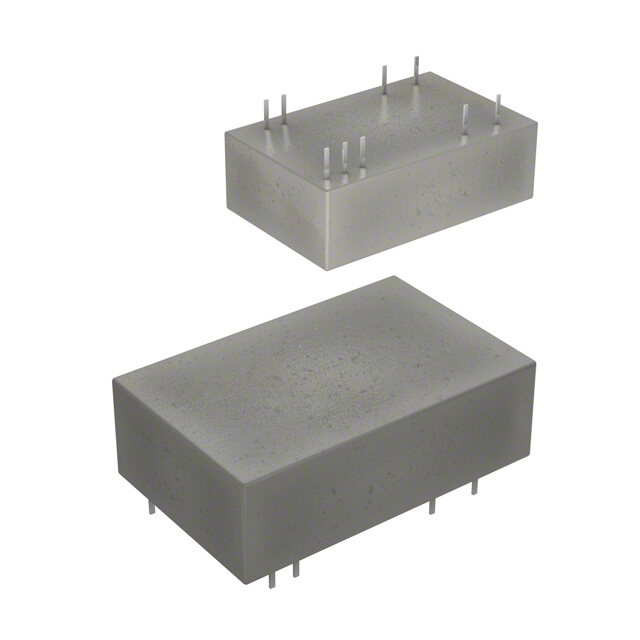
| 描述 | IC REG ISOLATED 5V 0.4A 7DIP隔离式DC/DC转换器 Mini 2W Iso Unreg DC/DC Converter |
| 产品分类 | DC DC ConvertersDC/DC转换器 |
| 品牌 | Texas Instruments |
| 产品手册 | |
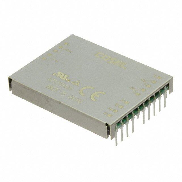
| 产品图片 |
|
| rohs | 符合RoHS无铅 / 符合限制有害物质指令(RoHS)规范要求 |
| 产品系列 | 隔离式DC/DC转换器,Texas Instruments DCP022405PDCP02 |
| 数据手册 | |
| 产品型号 | DCP022405P |
| 产品 | Isolated |
| 产品目录页面 | |
| 产品种类 | 隔离式DC/DC转换器 |
| 制造商产品页 | http://www.ti.com/general/docs/suppproductinfo.tsp?distId=10&orderablePartNumber=DCP022405P |
| 功率(W)-制造系列 | 2W |
| 功率(W)-最大值 | 65mW |
| 包装 | 管件 |
| 商标 | Texas Instruments |
| 大小/尺寸 | 0.78" 长 x 0.33" 宽 x 0.21" 高 (19.7mm x 8.3mm x 5.3mm) |
| 安装类型 | 通孔 |
| 安装风格 | Through Hole |
| 封装 | Tube |
| 封装/外壳 | 14-DIP(0.300",7.62mm),7 引线 |
| 封装/箱体尺寸 | PDIP-7 |
| 工作温度 | -40°C ~ 85°C |
| 工作温度范围 | - 40 C to + 85 C |
| 工厂包装数量 | 25 |
| 效率 | 81% |
| 标准包装 | 25 |
| 特性 | OTP |
| 电压-输入(最大值) | 26.4V |
| 电压-输入(最小值) | 21.6V |
| 电压-输出1 | 5V |
| 电压-输出2 | - |
| 电压-输出3 | - |
| 电压-隔离 | 1kV(1000V) |
| 电流-输出(最大值) | 400mA |
| 类型 | 隔离模块 |
| 系列 | DCP022405 |
| 输入电压范围 | 21.6 V to 26.4 V |
| 输出功率 | 2 W |
| 输出数 | 1 |
| 输出电压—通道1 | 5.35 V |
| 输出电流—通道1 | 400 mA |
| 输出端数量 | 1 |


- 商务部:美国ITC正式对集成电路等产品启动337调查
- 曝三星4nm工艺存在良率问题 高通将骁龙8 Gen1或转产台积电
- 太阳诱电将投资9.5亿元在常州建新厂生产MLCC 预计2023年完工
- 英特尔发布欧洲新工厂建设计划 深化IDM 2.0 战略
- 台积电先进制程称霸业界 有大客户加持明年业绩稳了
- 达到5530亿美元!SIA预计今年全球半导体销售额将创下新高
- 英特尔拟将自动驾驶子公司Mobileye上市 估值或超500亿美元
- 三星加码芯片和SET,合并消费电子和移动部门,撤换高东真等 CEO
- 三星电子宣布重大人事变动 还合并消费电子和移动部门
- 海关总署:前11个月进口集成电路产品价值2.52万亿元 增长14.8%

PDF Datasheet 数据手册内容提取
Product Sample & Technical Tools & Support & Folder Buy Documents Software Community DCP020503,DCP020505,DCP020507,DCP020509,DCP020515D,DCP021205 DCP021212,DCP021212D,DCP021515,DCP022405,DCP022405D,DCP022415D SBVS011L–MARCH2000–REVISEDMAY2015 DCP02x 2-W, Isolated, Unregulated DC/DC Converter Modules 1 Features 3 Description • 1-kVIsolation(Operational) The DCP02 series is a family of 2-W, isolated, 1 unregulated DC/DC converter modules. Requiring a • Device-to-DeviceSynchronization minimum of external components and including on- • EN55022ClassBEMCPerformance chip device protection, the DCP02 series of devices • UL1950RecognizedComponent provide extra features such as output disable and synchronizationofswitchingfrequencies. • 7-PinPDIPand12-PinSOPPackages This combination of features and small size makes 2 Applications theDCP02seriesofdevicessuitableforawiderange of applications, and is an easy-to-use solution in • SignalPathIsolation applicationsrequiringsignalpathisolation. • GroundLoopElimination WARNING: This product has operational isolation • DataAcquisition and is intended for signal isolation only. It should not • IndustrialControlandInstrumentation be used as a part of a safety isolation circuit requiring • TestEquipment reinforced isolation. See definitions in the Feature Descriptionsection. DeviceInformation(1) PARTNUMBER PACKAGE BODYSIZE(NOM) PDIP(7) 19.18mm×10.60mm DCP02xxxx SOP(12) 17.90mm×10.33mm (1) For all available packages, see the orderable addendum at theendofthedatasheet. . . SingleOutputBlockDiagram DualOutputBlockDiagram OSC Divide- OSC Divide- SYNC 800 by-2 +VOUT SYNC 800 by-2 +VOUT kHz Reset kHz Reset PSotawgeer ±VOUT PSotawgeer COM Watchdog Watchdog Startup Startup ±VOUT PSU PSU Thermal Thermal Shutdown Shutdown +VS +VS Power Controller Power Controller ±VS ±VS . . . . 1 An IMPORTANT NOTICE at the end of this data sheet addresses availability, warranty, changes, use in safety-critical applications, intellectualpropertymattersandotherimportantdisclaimers.PRODUCTIONDATA.
DCP020503,DCP020505,DCP020507,DCP020509,DCP020515D,DCP021205 DCP021212,DCP021212D,DCP021515,DCP022405,DCP022405D,DCP022415D SBVS011L–MARCH2000–REVISEDMAY2015 www.ti.com Table of Contents 1 Features.................................................................. 1 8.4 DeviceFunctionalModes........................................11 2 Applications........................................................... 1 9 ApplicationandImplementation........................ 13 3 Description............................................................. 1 9.1 ApplicationInformation............................................13 4 RevisionHistory..................................................... 2 9.2 TypicalApplication .................................................13 5 DeviceComparisonTable..................................... 3 10 PowerSupplyRecommendations..................... 16 6 PinConfigurationandFunctions......................... 4 11 Layout................................................................... 17 11.1 LayoutGuidelines.................................................17 7 Specifications......................................................... 5 11.2 LayoutExample....................................................17 7.1 AbsoluteMaximumRatings......................................5 12 DeviceandDocumentationSupport................. 19 7.2 ESDRatings ............................................................5 7.3 RecommendedOperatingConditions.......................5 12.1 DeviceSupport ....................................................19 7.4 ThermalInformation..................................................5 12.2 DocumentationSupport .......................................19 7.5 ElectricalCharacteristics...........................................6 12.3 CommunityResources..........................................19 7.6 SwitchingCharacteristics..........................................6 12.4 RelatedLinks........................................................20 7.7 TypicalCharacteristics..............................................7 12.5 Trademarks...........................................................20 12.6 ElectrostaticDischargeCaution............................20 8 DetailedDescription.............................................. 8 12.7 Glossary................................................................20 8.1 Overview...................................................................8 13 Mechanical,Packaging,andOrderable 8.2 FunctionalBlockDiagrams.......................................8 Information........................................................... 20 8.3 FeatureDescription...................................................9 4 Revision History ChangesfromRevisionK(February2008)toRevisionL Page • UpdatedFeatures .................................................................................................................................................................. 1 • AddedESDRatingstable,FeatureDescriptionsection,DeviceFunctionalModessection,Applicationand Implementationsection,PowerSupplyRecommendationssection,Layoutsection,DeviceandDocumentation Supportsection,andMechanical,Packaging,andOrderableInformationsection................................................................ 1 • AddedDualOutputBlockDiagram......................................................................................................................................... 1 • Renamedpin"0V"to"COM"(outputsidecommonpin)intable............................................................................................ 4 • Renamedpin"V "to"+V "(inputvoltagepin)intable.......................................................................................................... 4 S S • Renamedpin"0V"to"–V "(inputsidecommonpin)intable................................................................................................ 4 S • AddedRecommendedOperatingConditionstable................................................................................................................ 5 • AddedThermalInformationtable........................................................................................................................................... 5 • AddedinformationtotheISOLATIONsectionoftheElectricalCharacteristicstable ........................................................... 6 • AddedIsolationsectiontotheFeatureDescriptionsection................................................................................................... 9 • AddedatypicalapplicationdesigntotheApplicationInformationsection........................................................................... 13 2 SubmitDocumentationFeedback Copyright©2000–2015,TexasInstrumentsIncorporated ProductFolderLinks:DCP020503 DCP020505 DCP020507 DCP020509 DCP020515D DCP021205DCP021212 DCP021212D DCP021515 DCP022405 DCP022405D DCP022415D
DCP020503,DCP020505,DCP020507,DCP020509,DCP020515D,DCP021205 DCP021212,DCP021212D,DCP021515,DCP022405,DCP022405D,DCP022415D www.ti.com SBVS011L–MARCH2000–REVISEDMAY2015 5 Device Comparison Table OUTPUT DEVICE LOAD NOLOAD BARRIER INPUT EFFICIENCY VOLTAGE OUTPUT REGULATION CURRENT CAPACITANCE NDUEMVBICEER VOVLST(AVG)E VNOM7@5%VLSO(TAYDP)(V) C(UmRAR)E(N1)T 10%LOTAOD1(20)0% 0%IQ(LmOAA)D 100%(%L)OAD VISOC=ISO75(p0VF)rms MIN TYP MAX MIN TYP MAX MAX TYP MAX TYP TYP TYP DCP020503P 3.13 3.3 3.46 600 19 30 18 74 26 DCP020503U DCP020505P 4.75 5 5.25 400 14 20 18 80 22 DCP020505U DCP020507P 4.5 5 5.5 6.65 7 7.35 285 14 25 20 81 30 DCP020507U DCP020509P 8.55 9 9.45 222 12 20 23 82 31 DCP020509U DCP020515DP ±14.25 ±15 ±15.75 133(3) 11 20 27 85 24 DCP020515DU DCP021205P 4.75 5 5.25 400 7 15 14 83 33 DCP021205U DCP021212P 10.8 12 13.2 11.4 12 12.6 166 7 20 15 87 47 DCP021212U DCP021212DP ±11.4 ±12 ±12.6 166(3) 6 20 16 88 35 DCP021212DU DCP021515P 13.5 15 16.5 14.25 15 15.75 133 6 20 15 88 42 DCP021515U DCP022405P 4.75 5 5.25 400 6 15 13 81 33 DCP022405U DCP022405DP 21.6 24 26.4 ±4.75 ±5 ±5.25 400(3) 6 15 12 80 22 DCP022405DU DCP022415DP ±14.25 ±15 ±15.75 133(3) 6 25 16 79 44 DCP022415DU (1) P =2W OUT(max) (2) Loadregulation=(V at10%load–V at100%)/V at75%load OUT OUT OUT (3) I +I OUT1 OUT2 Copyright©2000–2015,TexasInstrumentsIncorporated SubmitDocumentationFeedback 3 ProductFolderLinks:DCP020503 DCP020505 DCP020507 DCP020509 DCP020515D DCP021205DCP021212 DCP021212D DCP021515 DCP022405 DCP022405D DCP022415D
DCP020503,DCP020505,DCP020507,DCP020509,DCP020515D,DCP021205 DCP021212,DCP021212D,DCP021515,DCP022405,DCP022405D,DCP022415D SBVS011L–MARCH2000–REVISEDMAY2015 www.ti.com 6 Pin Configuration and Functions NVAPackage NVAPackage 7-PinPDIP(SingleOutput) 7-PinPDIP(DualOutput) (TopView) (TopView) +VS 1 14 SYNC +VS 1 14 SYNC –VS 2 –VS 2 DCP02 DCP02 –V 5 COM 5 OUT +V 6 +V 6 OUT OUT NC 7 8 NC -V 7 8 NC OUT DVBPACKAGE DVBPackage 12-PinSOP(SingleOutput) 12-PinSOP(DualOutput) (TopView) (TopView) +VS 1 28 SYNC +VS 1 28 SYNC –VS 2 27 NC –VS 2 27 NC –VS 3 26 NC –VS 3 26 NC DCP02 DCP02 –V 12 17 NC COM 12 17 NC OUT +VOUT 13 16 NC +VOUT 13 16 NC NC 14 15 NC -VOUT 14 15 NC PinFunctions NUMBER PNIANME DVB DVB NVA NVA I/O(1) DESCRIPTION (DUAL) (SINGLE) (DUAL) (SINGLE) COM 12 — 5 — O Outputsidecommon 14 15 15 7 16 16 NC 8 — Noconnection 17 17 26 26 8 27 27 SynchronizationPin-Synchronizemultipledevicesbyconnecting SYNC 28 28 14 14 I theirSYNCpinstogether.Pullingthispinlowdisablestheinternal oscillator. +V 13 13 6 6 O Positiveoutputvoltage OUT –V 14 12 7 5 O Negativeoutputvoltage OUT +V 1 1 1 1 I Inputvoltage S 2 2 –V 2 2 I Inputsidecommon S 3 3 (1) I=Input,O=Output 4 SubmitDocumentationFeedback Copyright©2000–2015,TexasInstrumentsIncorporated ProductFolderLinks:DCP020503 DCP020505 DCP020507 DCP020509 DCP020515D DCP021205DCP021212 DCP021212D DCP021515 DCP022405 DCP022405D DCP022415D
DCP020503,DCP020505,DCP020507,DCP020509,DCP020515D,DCP021205 DCP021212,DCP021212D,DCP021515,DCP022405,DCP022405D,DCP022415D www.ti.com SBVS011L–MARCH2000–REVISEDMAY2015 7 Specifications 7.1 Absolute Maximum Ratings overoperatingfree-airtemperaturerange(unlessotherwisenoted) (1) MIN MAX UNIT 5-Vinputdevices 7 12-Vinputdevices 15 Inputvoltage V 15-Vinputdevices 18 24-Vinputdevices 29 Storagetemperature,T –60 125 °C stg (1) StressesbeyondthoselistedunderAbsoluteMaximumRatingsmaycausepermanentdamagetothedevice.Thesearestressratings only,whichdonotimplyfunctionaloperationofthedeviceattheseoranyotherconditionsbeyondthoseindicatedunderRecommended OperatingConditions.Exposuretoabsolute-maximum-ratedconditionsforextendedperiodsmayaffectdevicereliability. 7.2 ESD Ratings VALUE UNIT Human-bodymodel(HBM),perANSI/ESDA/JEDECJS-001(1) ±1000 V(ESD) Electrostaticdischarge Charged-devicemodel(CDM),perJEDECspecificationJESD22- V C101(2) ±250 (1) JEDECdocumentJEP155statesthat500-VHBMallowssafemanufacturingwithastandardESDcontrolprocess. (2) JEDECdocumentJEP157statesthat250-VCDMallowssafemanufacturingwithastandardESDcontrolprocess. 7.3 Recommended Operating Conditions overoperatingfree-airtemperaturerange(unlessotherwisenoted) MIN NOM MAX UNIT 5-Vinputdevices 4.5 5 5.5 12-Vinputdevices 10.8 12 13.2 InputVoltage V 15-Vinputdevices 13.5 15 16.5 24-Vinputdevices 21.6 24 26.4 Operatingtemperature –40 85 °C 7.4 Thermal Information DCP020x DCP020x THERMALMETRIC(1) NVA(PDIP) DVB(SOP) UNIT 7PINS 12PINS R Junction-to-ambientthermalresistance 61 61 θJA R Junction-to-case(top)thermalresistance 19 19 θJC(top) R Junction-to-boardthermalresistance 24 24 θJB °C/W ψ Junction-to-topcharacterizationparameter 7 7 JT ψ Junction-to-boardcharacterizationparameter 24 24 JB R Junction-to-case(bottom)thermalresistance N/A N/A θJC(bot) (1) Formoreinformationabouttraditionalandnewthermalmetrics,seetheSemiconductorandICPackageThermalMetricsapplication report,SPRA953. Copyright©2000–2015,TexasInstrumentsIncorporated SubmitDocumentationFeedback 5 ProductFolderLinks:DCP020503 DCP020505 DCP020507 DCP020509 DCP020515D DCP021205DCP021212 DCP021212D DCP021515 DCP022405 DCP022405D DCP022415D
DCP020503,DCP020505,DCP020507,DCP020509,DCP020515D,DCP021205 DCP021212,DCP021212D,DCP021515,DCP022405,DCP022405D,DCP022415D SBVS011L–MARCH2000–REVISEDMAY2015 www.ti.com 7.5 Electrical Characteristics overoperatingfree-airtemperaturerange(unlessotherwisenoted) PARAMETER TESTCONDITIONS MIN TYP MAX UNIT OUTPUT P Outputpower I =100%(fullload) 2 W OUT LOAD V Outputvoltageripple C =1μF,I =50% 20 mV RIPPLE OUT LOAD PP –40°C≤T ≤25°C 0.046 %/°C A Voltagevs.Temperature 25°C≤T ≤85°C 0.016 %/°C A INPUT V Inputvoltagerange –10% 10% S ISOLATION Voltage 1 kVrms 1-secondflashtest dV/dt 500 V/s V Isolation LeakageCurrent 30 nA ISO Continuousworking DC 60 VDC voltageacrossisolation barrier AC 42.5 VAC LINEREGULATION I ≥10%loadcurrentandconstant, OUT 1% 15% V (min)toV (typ) S S Outputvoltage I ≥10%loadcurrentandconstant, OUT 1% 15% V (typ)toV (max) S S RELIABILITY Demonstrated T =55°C 75 FITS A THERMALSHUTDOWN Dietemperatureat T 150 °C SD shutdown I Shutdowncurrent 3 mA SD 7.6 Switching Characteristics overoperatingfree-airtemperaturerange(unlessotherwisenoted) PARAMETER TESTCONDITIONS MIN TYP MAX UNIT f Oscillatorfrequency f =f /2 800 kHz OSC SW OSC V Low-levelinputvoltage,SYNC 0 0.4 V IL I Inputcurrent,SYNC V =2V 75 µA SYNC SYNC t Disabletime 2 µs DISABLE C CapacitanceloadingonSYNCpin(1) External 3 pF SYNC (1) TheapplicationreportExternalSynchronizationoftheDCP01/02SeriesofDC/DCConverters(SBAA035)describesthisconfiguration. 6 SubmitDocumentationFeedback Copyright©2000–2015,TexasInstrumentsIncorporated ProductFolderLinks:DCP020503 DCP020505 DCP020507 DCP020509 DCP020515D DCP021205DCP021212 DCP021212D DCP021515 DCP022405 DCP022405D DCP022415D
DCP020503,DCP020505,DCP020507,DCP020509,DCP020515D,DCP021205 DCP021212,DCP021212D,DCP021515,DCP022405,DCP022405D,DCP022415D www.ti.com SBVS011L–MARCH2000–REVISEDMAY2015 7.7 Typical Characteristics T =25°C,unlessotherwisenoted. A 60 5.04 Series 1 A) 50 Series 2 5.02 µ Series 3 B/ 40 el (d 30 e (V) 5.00 ev ag 4.98 k Emission L 12000 Output Volt 44..9964 a Pe ±10 4.92 ±20 4.90 0.15 1 10 30 ±40 ±20 0 20 40 60 80 100 Frequency (MHz) Temperature (°C) DCP020505P I =400mA DCP020505P 75%LoadCurrent LOAD Figure1.ConductedEmmisionsvs.Frequency Figure2.OutputVoltagevs.Temperature 5.4 2.5 5.3 2.0 V) W) oltage ( 5.2 ower ( 1.5 V P ut 5.1 ut 1.0 p p ut ut O O 5.0 0.5 4.9 0 0 20 40 60 80 100 ±50 ±25 0 25 50 75 100 Load (%) Temperature (°C) DCP021205P DCP021205P I =400mA LOAD Figure3.OutputVoltagevs.OutputCurrent Figure4.OutputPowervs.Temperature 100 450 COUT = 1 µF 400 80 )P-P 350 COUT = 0.1 µF V y (%) 60 ple (m 320500 c p cien 40 C Ri 200 Effi ut A 150 p 20 ut 100 O DCP021212DP 50 DCP021205P 0 0 0 25 50 75 100 0 100 200 300 400 Load (%) Load Current (mA) DCP020505P (20MHz bandwidth) Figure5.Efficiencyvs.PercentLoadCurrent Figure6.OutputACRipplevs.LoadCurrent Copyright©2000–2015,TexasInstrumentsIncorporated SubmitDocumentationFeedback 7 ProductFolderLinks:DCP020503 DCP020505 DCP020507 DCP020509 DCP020515D DCP021205DCP021212 DCP021212D DCP021515 DCP022405 DCP022405D DCP022415D
DCP020503,DCP020505,DCP020507,DCP020509,DCP020515D,DCP021205 DCP021212,DCP021212D,DCP021515,DCP022405,DCP022405D,DCP022415D SBVS011L–MARCH2000–REVISEDMAY2015 www.ti.com 8 Detailed Description 8.1 Overview The DCP02 offers up to 2 W of isolated, unregulated output power from a 5-V, 12-V, 15-V, or 24-V input source with a typical efficiency of up to 89%. This efficiency is achieved through highly integrated packaging technology and the implementation of a custom power stage and control device. The DCP02 devices are specified for operationalisolationonly.ThecircuitdesignusesanadvancedBiCMOS/DMOSprocess. 8.2 Functional Block Diagrams Oscillator Divide-by-2 +VOUT SYNC 800 kHz Reset Power Stage –VOUT Watchdog Startup PSU Thermal Shutdown +VS Power Controller –VS Figure7. SingleOutputDevice Oscillator Divide-by-2 +VOUT SYNC 800 kHz Reset Power COM Stage Watchdog Startup –VOUT PSU Thermal Shutdown +VS Power Controller –VS Figure8. DualOutputDevice 8 SubmitDocumentationFeedback Copyright©2000–2015,TexasInstrumentsIncorporated ProductFolderLinks:DCP020503 DCP020505 DCP020507 DCP020509 DCP020515D DCP021205DCP021212 DCP021212D DCP021515 DCP022405 DCP022405D DCP022415D
DCP020503,DCP020505,DCP020507,DCP020509,DCP020515D,DCP021205 DCP021212,DCP021212D,DCP021515,DCP022405,DCP022405D,DCP022415D www.ti.com SBVS011L–MARCH2000–REVISEDMAY2015 8.3 Feature Description 8.3.1 Isolation UnderwritersLaboratories,UL™definesseveralclassesofisolationthatareusedinmodernpowersupplies. Safety extra low voltage (SELV) is defined by UL (UL1950 E199929) as a secondary circuit which is so designated and protected that under normal and single fault conditions the voltage between any two accessible parts, or between an accessible part and the equipment earthing terminal for operational isolation does not exceedsteadystate42Vpeakor60V formorethan1second. DC 8.3.1.1 OperationorFunctionalIsolation Operational or functional isolation is defined by the use of a high-potential (hipot) test only. Typically, this isolation is defined as the use of insulated wire in the construction of the transformer as the primary isolation barrier. The hipot one-second duration test (dielectric voltage, withstand test) is a production test used to verify that the isolation barrier is functioning. Products with operational isolation should never be used as an element in asafety-isolationsystem. 8.3.1.2 BasicorEnhancedIsolation Basic or enhanced isolation is defined by specified creepage and clearance limits between the primary and secondarycircuitsofthepowersupply.Basicisolationistheuseofanisolationbarrierinadditiontotheinsulated wire in the construction of the transformer. Input and output circuits must also be physically separated by specifieddistances. 8.3.1.3 ContinuousVoltage For a device that has no specific safety agency approvals (operational isolation), the continuous voltage that can be applied across the part in normal operation is less than 42.4 V , or 60 V . Ensure that both input and RMS DC output voltages maintain normal SELV limits. The isolation test voltage represents a measure of immunity to transientvoltages. WARNING Do not use the device as an element of a safety isolation system when SELV is exceeded Ifthedeviceisexpectedtofunctioncorrectlywithmorethan42.4V or60V appliedcontinuouslyacrossthe RMS DC isolation barrier, then the circuitry on both sides of the barrier must be regarded as operating at an unsafe voltage, and further isolation or insulation systems must form a barrier between these circuits and any user- accessiblecircuitryaccordingtosafetystandardrequirements. 8.3.1.4 IsolationVoltage Hipot test, flash-tested, withstand voltage, proof voltage, dielectric withstand voltage, and isolation test voltage are all terms that relate to the same thing: a test voltage applied for a specified time across a component designed to provide electrical isolation to verify the integrity of that isolation. TI’s DCP02 series of dc-dc convertersareall100%productiontestedat1.0kV foronesecond. AC 8.3.1.5 RepeatedHigh-VoltageIsolationTesting Repeatedhigh-voltageisolationtestingofabarriercomponentcandegradetheisolationcapability,dependingon materials, construction, and environment. The DCP02 series of dc-dc converters have toroidal, enameled, wire isolation transformers with no additional insulation between the primary and secondary windings. While a device can be expected to withstand several times the stated test voltage, the isolation capability depends on the wire insulation. Any material, including this enamel (typically polyurethane), is susceptible to eventual chemical degradation when subject to very-high applied voltages. Therefore, strictly limit the number of high-voltage tests and repeated high-voltage isolation testing. However, if it is absolutely required, reduce the voltage by 20% from specifiedtestvoltagewithadurationlimitofonesecondpertest. Copyright©2000–2015,TexasInstrumentsIncorporated SubmitDocumentationFeedback 9 ProductFolderLinks:DCP020503 DCP020505 DCP020507 DCP020509 DCP020515D DCP021205DCP021212 DCP021212D DCP021515 DCP022405 DCP022405D DCP022415D
DCP020503,DCP020505,DCP020507,DCP020509,DCP020515D,DCP021205 DCP021212,DCP021212D,DCP021515,DCP022405,DCP022405D,DCP022415D SBVS011L–MARCH2000–REVISEDMAY2015 www.ti.com Feature Description (continued) 8.3.2 PowerStage The DCP02 series of devices use a push-pull, center-tapped topology. The DCP02 devices switch at 400 kHz (divide-by-2froman800-kHzoscillator). 8.3.3 OscillatorAndWatchdogCircuit The onboard, 800-kHz oscillator generates the switching frequency via a divide-by-2 circuit. The oscillator can be synchronizedtootherDCP02-seriesdevicecircuitsoranexternalsource,andisusedtominimizesystemnoise. A watchdog circuit checks the operation of the oscillator circuit. The oscillator can be disabled by pulling the SYNC pin low. When the SYNC pin goes low, the output pins transition into tri-state mode, which occurs within 2μs. 8.3.4 ThermalShutdown TheDCP02seriesofdevicesareprotectedbyathermal-shutdowncircuit. If the on-chip temperature rises above 150°C, the device shuts down. Normal operation resumes as soon as the temperaturefallsbelow150°C. 8.3.5 Synchronization In the event that more than one DC/DC converter is needed onboard, beat frequencies and other electrical interference can be generated. This interference occurs because of the small variations in switching frequencies betweentheDC/DCconverters. The DCP02 series of devices overcome this interference by allowing devices to be synchronized to one another. Up to eight devices can be synchronized by connecting the SYNC pins together, taking care to minimize the capacitance of tracking. Stray capacitance (greater than 3 pF) has the effect of reducing the switching frequency, orevenstoppingtheoscillatorcircuit.ThemaximumrecommendedvoltageappliedtotheSYNCpinis3.0V. For an application that uses more than eight synchronized devices use an external device to drive the SYNC pins. The application report External Synchronization of the DCP01/02 Series of DC/DC Converters (SBAA035) describesthisconfiguration. NOTE During the start-up period, all synchronized devices draw maximum current from the input simultaneously. If the input voltage falls below approximately 4 V, the devices may not start up. A 2.2-μF capacitor should be connected close to each device'sinputpin. 8.3.6 Construction The basic construction of the DCP02 series of devices is the same as standard integrated circuits. The molded package contains no substrate. The DCP02 series of devices are constructed using an IC, rectifier diodes, and a wound magnetic toroid on a leadframe. Because the package contains no solder, the devices do not require any specialprintedcircuitboard(PCB)assemblyprocessing.ThisarchitectureresultsinanisolatedDC/DCconverter withinherentlyhighreliability. 8.3.7 ThermalManagement Duetothehighpowerdensityofthisdevice,itisadvisabletoprovidegroundplanesontheinputandoutput. 10 SubmitDocumentationFeedback Copyright©2000–2015,TexasInstrumentsIncorporated ProductFolderLinks:DCP020503 DCP020505 DCP020507 DCP020509 DCP020515D DCP021205DCP021212 DCP021212D DCP021515 DCP022405 DCP022405D DCP022415D
DCP020503,DCP020505,DCP020507,DCP020509,DCP020515D,DCP021205 DCP021212,DCP021212D,DCP021515,DCP022405,DCP022405D,DCP022415D www.ti.com SBVS011L–MARCH2000–REVISEDMAY2015 8.4 Device Functional Modes 8.4.1 Disable/Enable(SYNCpin) Any of the DCP02 series devices can be disabled or enabled by driving the SYNC pin using an open drain CMOS gate. If the SYNC pin is pulled low, the DCP02 becomes disabled. The disable time depends upon the external loading. The internal disable function is implemented in 2 μs. Removal of the pull down causes the DCP02tobeenabled. Capacitive loading on the SYNC pin should be minimized (≤ 3 pF) in order to prevent a reduction in the oscillator frequency. The application report External Synchronization of the DCP01/02 Series of DC/DC Converters (SBAA035) describesdisable/enablecontrolcircuitry. 8.4.2 Decoupling 8.4.2.1 RippleReduction The high switching frequency of 400 kHz allows simple filtering. To reduce ripple, it is recommended that a minimum of 1-μF capacitor be used on the V pin. For dual output devices, decouple both of the outputs to the OUT COMpin.A2.2-μFcapacitorontheinputisalsorecommended. 8.4.2.2 ConnectingtheDCP02inSeries Multiple DCP02 isolated 2W DC/DC converters can be connected in series to provide non-standard voltage rails. ThisconfigurationispossiblebyusingthefloatingoutputsprovidedbythegalvanicisolationoftheDCP02. Connect the +V from one DCP02 to the –V of another (see Figure 9). If the SYNC pins are tied together, OUT OUT the self-synchronization feature of the DCP02 prevents beat frequencies on the voltage rails. The SYNC feature oftheDCP02allowseasyseriesconnectionwithoutexternalfiltering,thusminimizingcost. Theoutputsofadual-outputDCP02canalsobeconnectedinseriestoprovidetwotimesthemagnitudeofV , OUT asshowninFigure10.Forexample,connectadual-output,15-V,DCP022415Ddevicetoprovidea30-Vrail. All 5-V, 12-V, and 15-V input voltage designs require a2.2-μF, low-ESR ceramic input capacitor, while 24-V input applicationsrequireonly0.47μFofinputcapacitance. VIN +VS +VOUT1 CIN COUT SYNC DCP 02 1.0 µF –VS –VOUT1 VOUT1 + VOUT2 VS +VOUT2 CIN COUT SYNC DCP 02 1.0 µF –VS –VOUT2 Figure9. MultipleDCP02DevicesConnectedinSeries VIN +VS +VOUT +VOUT COUT CIN DCP 02 1.0 µF –VOUT –VOUT COUT 1.0 µF –VS COM Figure10. DualOutputDevicesConnectedinSeries Copyright©2000–2015,TexasInstrumentsIncorporated SubmitDocumentationFeedback 11 ProductFolderLinks:DCP020503 DCP020505 DCP020507 DCP020509 DCP020515D DCP021205DCP021212 DCP021212D DCP021515 DCP022405 DCP022405D DCP022415D
DCP020503,DCP020505,DCP020507,DCP020509,DCP020515D,DCP021205 DCP021212,DCP021212D,DCP021515,DCP022405,DCP022405D,DCP022415D SBVS011L–MARCH2000–REVISEDMAY2015 www.ti.com 8.4.2.3 ConnectingtheDCP02inParallel If the output power from one DCP02 is not sufficient, it is possible to parallel the outputs of multiple DCP02s, as shown in Figure 11, ( applies to single output devices only). The SYNC feature allows easy synchronization to preventpower-railbeatfrequenciesatnoadditionalfilteringcost. All 5-V, 12-V, and 15-V input voltage designs require a 2.2-μF, low-ESR, ceramic input capacitor, while 24-V inputapplicationsrequireonly0.47 μFofinputcapacitance. VIN +VS +VOUT1 SYNC DCP 02 COUT CIN 1.0 µF –VS –VOUT1 2 × Power Out +VS +VOUT2 DCP 02 COUT CIN SYNC 1.0 µF –VS –VOUT2 GND Figure11. MultipleDCP02DevicesConnectedinParallel 12 SubmitDocumentationFeedback Copyright©2000–2015,TexasInstrumentsIncorporated ProductFolderLinks:DCP020503 DCP020505 DCP020507 DCP020509 DCP020515D DCP021205DCP021212 DCP021212D DCP021515 DCP022405 DCP022405D DCP022415D
DCP020503,DCP020505,DCP020507,DCP020509,DCP020515D,DCP021205 DCP021212,DCP021212D,DCP021515,DCP022405,DCP022405D,DCP022415D www.ti.com SBVS011L–MARCH2000–REVISEDMAY2015 9 Application and Implementation NOTE Information in the following applications sections is not part of the TI component specification, and TI does not warrant its accuracy or completeness. TI’s customers are responsible for determining suitability of components for their purposes. Customers should validateandtesttheirdesignimplementationtoconfirmsystemfunctionality. 9.1 Application Information 9.2 Typical Application VIN +VS +VOUT +VOUT CIN SYNC DCP02 COUT 2.2 µF 1.0 µF –VS –VOUT –VOUT Figure12. TypicalDCP020505Application 9.2.1 DesignRequirements For this design example, use the parameters listed in Table 1 and follow the design procedures shown in DetailedDesignProceduresection. Table1.DesignExampleParameters PARAMETER VALUE UNIT V Inputvoltage 5 V (+VS) V Outputvoltage 5 V (+VOUT) I Outputcurrentrating 400 mA OUT f Operatingfrequency 400 kHz SW 9.2.2 DCP020505ApplicationCurves 100 5.9 90 5.7 80 V) 5.5 %) 70 e ( Efficiency ( 5600 utput Voltag 55..13 O 4.9 40 4.7 30 20 4.5 0 20 40 60 80 100 0 20 40 60 80 100 Load Current (%) C001 Load Current (%) C004 DCP020505Efficiency DCP020505LoadRegulation Figure13.DCP020505Efficiency Figure14.DCP020505LoadRegulation Copyright©2000–2015,TexasInstrumentsIncorporated SubmitDocumentationFeedback 13 ProductFolderLinks:DCP020503 DCP020505 DCP020507 DCP020509 DCP020515D DCP021205DCP021212 DCP021212D DCP021515 DCP022405 DCP022405D DCP022415D
DCP020503,DCP020505,DCP020507,DCP020509,DCP020515D,DCP021205 DCP021212,DCP021212D,DCP021515,DCP022405,DCP022405D,DCP022415D SBVS011L–MARCH2000–REVISEDMAY2015 www.ti.com 9.2.3 DetailedDesignProcedure 9.2.3.1 InputCapacitor For all 5-V, 12-V, and 15-V input voltage designs, select a 2.2-μF low-ESR ceramic input capacitor to ensure a goodstartupperformance.24-Vinputapplicationsrequireonly0.47-μFofinputcapacitance. 9.2.3.2 OutputCapacitor ForanyDCP02design,selecta1.0-μFlow-ESRceramicoutputcapacitortoreduceoutputripple. 9.2.3.3 SYNCPin Inastand-aloneapplication,leavetheSYNCpinfloating. 9.2.4 PCBDesign The copper losses (resistance and inductance) can be minimized by the use of mutual ground and power planes (tracks) where possible. If that is not possible, use wide tracks to reduce the losses. If several devices are being powered from a common power source, a star-connected system for the track must be deployed; devices must not be connected in series, as this will cascade the resistive losses. The position of the decoupling capacitors is important. They must be as close to the devices as possible in order to reduce losses. See the PCB Layout sectionformoredetails. 9.2.5 DecouplingCeramicCapacitors All capacitors have losses because of internal equivalent series resistance (ESR), and to a lesser degree, equivalent series inductance (ESL). Values for ESL are not always easy to obtain. However, some manufacturers provide graphs of frequency versus capacitor impedance. These graphs typically show the capacitor impedance falling as frequency is increased (as shown in Figure 15). In Figure 15, X is the reactance C due to the capacitance, X is the reactance due to the ESL, and f is the resonant frequency. As the frequency L 0 increases, the impedance stops decreasing and begins to rise. The point of minimum impedance indicates the resonant frequency of the capacitor. This frequency is where the components of capacitance and inductance reactanceareofequalmagnitude.Beyondthispoint,thecapacitorisnoteffectiveasacapacitor. Ÿ ) ce (Z n a d e p m pacitor I XC XL a C 0 f0 Frequency (Hz) Figure15. CapacitorImpedancevsFrequency At f , X = X ; however, there is a 180° phase difference resulting in cancellation of the imaginary component. 0 C L The resulting effect is that the impedance at the resonant point is the real part of the complex impedance; namely, the value of the ESR. The resonant frequency must be well above the 800-kHz switching frequency of theDCPandDCVs. 14 SubmitDocumentationFeedback Copyright©2000–2015,TexasInstrumentsIncorporated ProductFolderLinks:DCP020503 DCP020505 DCP020507 DCP020509 DCP020515D DCP021205DCP021212 DCP021212D DCP021515 DCP022405 DCP022405D DCP022415D
DCP020503,DCP020505,DCP020507,DCP020509,DCP020515D,DCP021205 DCP021212,DCP021212D,DCP021515,DCP022405,DCP022405D,DCP022415D www.ti.com SBVS011L–MARCH2000–REVISEDMAY2015 The effect of the ESR is to cause a voltage drop within the capacitor. The value of this voltage drop is simply the productoftheESRandthetransientloadcurrent,asshowninEquation1. V =V –(ESR×I ) IN PK TR where • V isthevoltageatthedeviceinput IN • V isthemaximumvalueofthevoltageonthecapacitorduringcharge PK • I isthetransientloadcurrent (1) TR The other factor that affects the performance is the value of the capacitance. However, for the input and the full waveoutputs(single-outputvoltagedevices),ESRisthedominantfactor. 9.2.6 InputCapacitorandtheEffectsofESR If the input decoupling capacitor is not ceramic (and has an ESR greater than 20 mΩ), then at the instant the power transistors switch on, the voltage at the input pins falls momentarily. If the voltage falls below approximately 4 V, the DCP detects an undervoltage condition and switches the DCP drive circuits to the off state. This detection is carried out as a precaution against a genuine low input voltage condition that could slow down or even stop the internal circuits from operating correctly. A slow-down or stoppage results in the drive transistorsbeingturnedontoolong,causingsaturationofthetransformeranddestructionofthedevice. Following detection of a low input voltage condition, the device switches off the internal drive circuits until the input voltage returns to a safe value, at which time the device tries to restart. If the input capacitor is still unable to maintain the input voltage, shutdown recurs. This process repeats until the input capacitor charges sufficiently tostartthedevicecorrectly. Normal startup should occur in approximately 1 ms after power is applied to the device. If a considerably longer startup duration time is encountered, it is likely that either (or both) the input supply or the capacitors are not performingadequately. For5-Vto15-Vinputdevices,a2.2-μF,low-ESRceramiccapacitorensuresagoodstartupperformance.For24- V input voltage devices, 0.47 μF ceramic capacitors are recommended. Tantalum capacitors are not recommended, since most do not have low-ESR values and will degrade performance. If tantalum capacitors mustbeused,closeattentionmustbepaidtoboththeESRandvoltageasderatedbythevendor. NOTE Duringthestart-upperiod,thesedevicesmaydrawmaximumcurrentfromtheinput supply. If the input voltage falls below approximately 4 V, the devices may not start up.Connecta2.2-μFceramiccapacitorclosetotheinputpins. 9.2.7 RippleandNoise A good quality, low-ESR ceramic capacitor placed as close as practical across the input reduces reflected ripple andensuresasmoothstartup. A good quality, low-ESR ceramic capacitor placed as close as practical across the rectifier output terminal and output ground gives the best ripple and noise performance. See DC-to-DC Converter Noise Reduction (SBVA012),formoreinformationonnoiserejection. 9.2.7.1 OutputRippleCalculationExample The following example shows that increasing the capacitance has a much smaller effect on the output ripple voltagethandoesreducingthevalueoftheESRforthefiltercapacitor. TocalculatetheoutputrippleforaDCP020505device: • V =5V OUT • I =0.4A OUT • Atfulloutputpower,theloadresistoris12.5Ω • Outputcapacitorof1μF,ESRof0.1Ω • Capacitordischargetime1%of800kHz(ripplefrequency t =0.0125μs DIS Copyright©2000–2015,TexasInstrumentsIncorporated SubmitDocumentationFeedback 15 ProductFolderLinks:DCP020503 DCP020505 DCP020507 DCP020509 DCP020515D DCP021205DCP021212 DCP021212D DCP021515 DCP022405 DCP022405D DCP022415D
DCP020503,DCP020505,DCP020507,DCP020509,DCP020515D,DCP021205 DCP021212,DCP021212D,DCP021515,DCP022405,DCP022405D,DCP022415D SBVS011L–MARCH2000–REVISEDMAY2015 www.ti.com τ=C ×R LOAD τ=1×10-6×12.5=12.5μs V =V (1– EXP(–t /τ)) DIS O DIS V =5mV DIS Bycontrast,thevoltagedroppedbecauseofESR: V =I ×ESR ESR LOAD V =40mV ESR Ripplevoltage=45mV 9.2.8 DualDCP02OutputVoltage The voltage output for dual DCP02 devices is half wave rectified; therefore, the discharge time is 1.25 μs. Repeatingtheabovecalculationsusingthe100%loadresistanceof25Ω (0.2Aperoutput),theresultsare: τ=25 μs t =1.25 μs DIS V =244mV DIS V =20mV ESR RippleVoltage=266mV This time, it is the capacitor discharging that contributes to the largest component of ripple. Changing the output filterto10μF,andrepeatingthecalculations,theresultis: RippleVoltage=45mV. Thisvalueiscomposedofalmostequalcomponents. The previous calculations are offered as a guideline only. Capacitor parameters usually have large tolerances andcanbesusceptibletoenvironmentalconditions. 9.2.9 OptimizingPerformance Optimum performance can only be achieved if the device is correctly supported. The very nature of a switching converter requires power to be instantly available when it switches on. If the converter has DMOS switching transistors, the fast edges will create a high current demand on the input supply. This transient load placed on the input is supplied by the external input decoupling capacitor, thus maintaining the input voltage. Therefore, the input supply does not see this transient (this is an analogy to high-speed digital circuits). The positioning of the capacitoriscriticalandmustbeplacedascloseaspossibletotheinputpinsandconnectedviaalow-impedance path. Theoptimumperformanceprimarilydependsontwofactors: • Connectionoftheinputandoutputcircuitsforminimalloss. • Theabilityofthedecouplingcapacitorstomaintaintheinputandoutputvoltagesataconstantlevel. 10 Power Supply Recommendations The DCP02 is a switching power supply, and as such can place high peak current demands on the input supply. Inordertoavoidthesupplyfallingmomentarilyduringthefastswitchingpulses,groundandpowerplanesshould be used to connect the power to the input of DCP02. If this connection is not possible, then the supplies must be connectedinastarformationwiththetracesmadeaswideaspossible. 16 SubmitDocumentationFeedback Copyright©2000–2015,TexasInstrumentsIncorporated ProductFolderLinks:DCP020503 DCP020505 DCP020507 DCP020509 DCP020515D DCP021205DCP021212 DCP021212D DCP021515 DCP022405 DCP022405D DCP022415D
DCP020503,DCP020505,DCP020507,DCP020509,DCP020515D,DCP021205 DCP021212,DCP021212D,DCP021515,DCP022405,DCP022405D,DCP022415D www.ti.com SBVS011L–MARCH2000–REVISEDMAY2015 11 Layout 11.1 Layout Guidelines Duetothehighpowerdensityofthesedevices,providegroundplanesontheinputandoutput. Figure 19 and Figure 17 illustrate a printed circuit board (PCB) layout for the two conventional (DCP01/02, DCV01),andtwoSOPsurface-mountpackages(DCP02U).Figure16 showstheschematic. Including input power and ground planes provides a low-impedance path for the input power. For the output, the COM signal connects via a ground plane, while the connections for the positive and negative voltage outputs conductviawidetracesinordertominimizelosses. Theoutputshouldbetakenfromthedeviceusinggroundandpowerplanes,therebyensuringminimumlosses. Thelocationofthedecouplingcapacitorsincloseproximitytotheirrespectivepinsensureslowlossesduetothe effects of stray inductance, thus improving the ripple performance. This location is of particular importance to the input decoupling capacitor, because this capacitor supplies the transient current associated with the fast switchingwaveformsofthepowerdrivecircuits. Allow the unused SYNC pin, to remain configured as a floating pad. It is advisable to place a guard ring (connected to input ground) or annulus connected around this pin to avoid any noise pick up. When connecting a SYNC pin to one or more SYNC design the linking trace to be short and narrow to avoid stray capacitance. Ensure that no other trace is in close proximity to this trace SYNC trace to decrease the stray capacitance on thispin.Thestraycapacitanceaffectstheperformanceoftheoscillator. 11.2 Layout Example CON1 CON3 VS1 1 +VS SYNC 14 JP1 VS3 1 +VS SYNC 28 JP1 C1 C11 NC 27 0V1 2 –VS 0V3 2 –VS NC 26 DCP02xxxxP 3 –VS +V1 C3 C2-1 C2 6 +VOUT +V3 13 +VOUT C13 C12 R1 R5 DCP02xxxxU 5 COM 12 COM COM1 C5 C4-1 C4 COM3 C14 C15 R2 R6 – V1 7 –VOUT – V3 14 –VOUT CON2 CON4 VS2 1 +VS SYNC 14 JP2 VS4 1 +VS SYNC 28 JP2 C6 C16 NC 27 0V2 2 –VS 0V4 2 –VS NC 26 DCP02xxxxP 3 –VS +V2 C8 C7-1 C7 6 +VOUT +V4 13 +VOUT C17 C18 R3 R7 DCP02xxxxU 5 COM 12 COM COM2 C10 C9-1 C9 COM4 C20 C19 R4 R8 – V2 7 –VOUT – V4 14 –VOUT Figure16.PCBSchematic,PPackage Figure17.PCBSchematic,UPackage Copyright©2000–2015,TexasInstrumentsIncorporated SubmitDocumentationFeedback 17 ProductFolderLinks:DCP020503 DCP020505 DCP020507 DCP020509 DCP020515D DCP021205DCP021212 DCP021212D DCP021515 DCP022405 DCP022405D DCP022415D
DCP020503,DCP020505,DCP020507,DCP020509,DCP020515D,DCP021205 DCP021212,DCP021212D,DCP021515,DCP022405,DCP022405D,DCP022415D SBVS011L–MARCH2000–REVISEDMAY2015 www.ti.com Layout Example (continued) Figure18. PCBLayoutExample,Component-SideView Figure19. PCBLayoutExample,Non-Component-SideView 18 SubmitDocumentationFeedback Copyright©2000–2015,TexasInstrumentsIncorporated ProductFolderLinks:DCP020503 DCP020505 DCP020507 DCP020509 DCP020515D DCP021205DCP021212 DCP021212D DCP021515 DCP022405 DCP022405D DCP022415D
DCP020503,DCP020505,DCP020507,DCP020509,DCP020515D,DCP021205 DCP021212,DCP021212D,DCP021515,DCP022405,DCP022405D,DCP022415D www.ti.com SBVS011L–MARCH2000–REVISEDMAY2015 12 Device and Documentation Support 12.1 Device Support 12.1.1 DeviceNomenclature DCP02 05 03 (D) (P) Basic model number: 2-W product Voltage input: 5, 12,15, or 24 Voltage output: 3, 5, 7, 9 or 15 Output type: S (single) or D (dual) Package code: P = 7-pin PDIP (NVA package) U = 12-pin SOP (DVB package) Figure20. SupplementalOrderingInformation 12.2 Documentation Support 12.2.1 RelatedDocumentation DC-to-DCConverterNoiseReduction(SBVA012) ExternalSynchronizationoftheDCP01/02SeriesofDC/DCConverters (SBAA035) OptimizingPerformanceoftheDCP01/02SeriesofDC/DCConverters (SBVA013) 12.3 Community Resources The following links connect to TI community resources. Linked contents are provided "AS IS" by the respective contributors. They do not constitute TI specifications and do not necessarily reflect TI's views; see TI's Terms of Use. TIE2E™OnlineCommunity TI'sEngineer-to-Engineer(E2E)Community.Createdtofostercollaboration amongengineers.Ate2e.ti.com,youcanaskquestions,shareknowledge,exploreideasandhelp solveproblemswithfellowengineers. DesignSupport TI'sDesignSupport QuicklyfindhelpfulE2Eforumsalongwithdesignsupporttoolsand contactinformationfortechnicalsupport. Copyright©2000–2015,TexasInstrumentsIncorporated SubmitDocumentationFeedback 19 ProductFolderLinks:DCP020503 DCP020505 DCP020507 DCP020509 DCP020515D DCP021205DCP021212 DCP021212D DCP021515 DCP022405 DCP022405D DCP022415D
DCP020503,DCP020505,DCP020507,DCP020509,DCP020515D,DCP021205 DCP021212,DCP021212D,DCP021515,DCP022405,DCP022405D,DCP022415D SBVS011L–MARCH2000–REVISEDMAY2015 www.ti.com 12.4 Related Links The table below lists quick access links. Categories include technical documents, support and community resources,toolsandsoftware,andquickaccesstosampleorbuy. Table2.RelatedLinks TECHNICAL TOOLS& SUPPORT& PARTS PRODUCTFOLDER SAMPLE&BUY DOCUMENTS SOFTWARE COMMUNITY DCP020503 Clickhere Clickhere Clickhere Clickhere Clickhere DCP020505 Clickhere Clickhere Clickhere Clickhere Clickhere DCP020507 Clickhere Clickhere Clickhere Clickhere Clickhere DCP020509 Clickhere Clickhere Clickhere Clickhere Clickhere DCP020515D Clickhere Clickhere Clickhere Clickhere Clickhere DCP021205 Clickhere Clickhere Clickhere Clickhere Clickhere DCP021212 Clickhere Clickhere Clickhere Clickhere Clickhere DCP021212D Clickhere Clickhere Clickhere Clickhere Clickhere DCP021515 Clickhere Clickhere Clickhere Clickhere Clickhere DCP022405 Clickhere Clickhere Clickhere Clickhere Clickhere DCP022405D Clickhere Clickhere Clickhere Clickhere Clickhere DCP022415D Clickhere Clickhere Clickhere Clickhere Clickhere 12.5 Trademarks E2EisatrademarkofTexasInstruments. UnderwritersLaboratories,ULaretrademarksofULLLC. Allothertrademarksarethepropertyoftheirrespectiveowners. 12.6 Electrostatic Discharge Caution Thesedeviceshavelimitedbuilt-inESDprotection.Theleadsshouldbeshortedtogetherorthedeviceplacedinconductivefoam duringstorageorhandlingtopreventelectrostaticdamagetotheMOSgates. 12.7 Glossary SLYZ022—TIGlossary. Thisglossarylistsandexplainsterms,acronyms,anddefinitions. 13 Mechanical, Packaging, and Orderable Information The following pages include mechanical, packaging, and orderable information. This information is the most current data available for the designated devices. This data is subject to change without notice and revision of thisdocument.Forbrowser-basedversionsofthisdatasheet,refertotheleft-handnavigation. 20 SubmitDocumentationFeedback Copyright©2000–2015,TexasInstrumentsIncorporated ProductFolderLinks:DCP020503 DCP020505 DCP020507 DCP020509 DCP020515D DCP021205DCP021212 DCP021212D DCP021515 DCP022405 DCP022405D DCP022415D
PACKAGE OPTION ADDENDUM www.ti.com 6-Feb-2020 PACKAGING INFORMATION Orderable Device Status Package Type Package Pins Package Eco Plan Lead/Ball Finish MSL Peak Temp Op Temp (°C) Device Marking Samples (1) Drawing Qty (2) (6) (3) (4/5) DCP020503P ACTIVE PDIP NVA 7 25 Pb-Free NIPDAU N / A for Pkg Type -40 to 85 DCP020503P (RoHS) DCP020503U ACTIVE SOP DVB 12 28 Pb-Free NIPDAU Level-3-260C-168 HR -40 to 85 DCP020503U (RoHS) DCP020505P ACTIVE PDIP NVA 7 25 Pb-Free NIPDAU N / A for Pkg Type -40 to 85 DCP020505P (RoHS) DCP020505U ACTIVE SOP DVB 12 28 Pb-Free NIPDAU Level-3-260C-168 HR -40 to 85 DCP020505U (RoHS) DCP020505U/1K ACTIVE SOP DVB 12 1000 Pb-Free NIPDAU Level-3-260C-168 HR -40 to 85 DCP020505U (RoHS) DCP020505UE4 ACTIVE SOP DVB 12 28 Pb-Free NIPDAU Level-3-260C-168 HR -40 to 85 DCP020505U (RoHS) DCP020507P ACTIVE PDIP NVA 7 25 Pb-Free NIPDAU N / A for Pkg Type -40 to 85 DCP020507P (RoHS) DCP020507U ACTIVE SOP DVB 12 28 Pb-Free NIPDAU Level-3-260C-168 HR -40 to 85 DCP020507U (RoHS) DCP020507U/1K ACTIVE SOP DVB 12 1000 Pb-Free NIPDAU Level-3-260C-168 HR -40 to 85 DCP020507U (RoHS) DCP020509P ACTIVE PDIP NVA 7 25 Pb-Free NIPDAU N / A for Pkg Type -40 to 85 DCP020509P (RoHS) DCP020509U ACTIVE SOP DVB 12 28 Pb-Free NIPDAU Level-3-260C-168 HR -40 to 85 DCP020509U (RoHS) DCP020515DP ACTIVE PDIP NVA 7 25 Pb-Free NIPDAU N / A for Pkg Type -40 to 85 DCP020515DP (RoHS) DCP020515DU ACTIVE SOP DVB 12 28 Pb-Free NIPDAU Level-3-260C-168 HR -40 to 85 DCP020515DU (RoHS) DCP020515DU/1K ACTIVE SOP DVB 12 1000 Pb-Free NIPDAU Level-3-260C-168 HR -40 to 85 DCP020515DU (RoHS) DCP021205P ACTIVE PDIP NVA 7 25 Pb-Free NIPDAU N / A for Pkg Type -40 to 85 DCP021205P (RoHS) DCP021205PE4 ACTIVE PDIP NVA 7 25 Pb-Free NIPDAU N / A for Pkg Type -40 to 85 DCP021205P (RoHS) DCP021205U ACTIVE SOP DVB 12 28 Pb-Free NIPDAU Level-3-260C-168 HR -40 to 85 DCP021205U (RoHS) Addendum-Page 1
PACKAGE OPTION ADDENDUM www.ti.com 6-Feb-2020 Orderable Device Status Package Type Package Pins Package Eco Plan Lead/Ball Finish MSL Peak Temp Op Temp (°C) Device Marking Samples (1) Drawing Qty (2) (6) (3) (4/5) DCP021205U/1K ACTIVE SOP DVB 12 1000 Pb-Free NIPDAU Level-3-260C-168 HR -40 to 85 DCP021205U (RoHS) DCP021212DP ACTIVE PDIP NVA 7 25 Pb-Free NIPDAU N / A for Pkg Type -40 to 85 DCP021212DP (RoHS) DCP021212DU ACTIVE SOP DVB 12 28 Pb-Free NIPDAU Level-3-260C-168 HR -40 to 85 DCP021212DU (RoHS) DCP021212DU/1K ACTIVE SOP DVB 12 1000 Pb-Free NIPDAU Level-3-260C-168 HR -40 to 85 DCP021212DU (RoHS) DCP021212P ACTIVE PDIP NVA 7 25 Pb-Free NIPDAU N / A for Pkg Type -40 to 85 DCP021212P (RoHS) DCP021212U ACTIVE SOP DVB 12 28 Pb-Free NIPDAU Level-3-260C-168 HR -40 to 85 DCP021212U (RoHS) DCP021212U/1K ACTIVE SOP DVB 12 1000 Pb-Free NIPDAU Level-3-260C-168 HR -40 to 85 DCP021212U (RoHS) DCP021515P ACTIVE PDIP NVA 7 25 Pb-Free NIPDAU N / A for Pkg Type -40 to 85 DCP021515P (RoHS) DCP021515U ACTIVE SOP DVB 12 28 Pb-Free NIPDAU Level-3-260C-168 HR -40 to 85 DCP021515U (RoHS) DCP021515U/1K ACTIVE SOP DVB 12 1000 Pb-Free NIPDAU Level-3-260C-168 HR -40 to 85 DCP021515U (RoHS) DCP022405DP ACTIVE PDIP NVA 7 25 Pb-Free NIPDAU N / A for Pkg Type -40 to 85 DCP022405DP (RoHS) DCP022405DU ACTIVE SOP DVB 12 28 Pb-Free NIPDAU Level-3-260C-168 HR -40 to 85 DCP022405DU (RoHS) DCP022405P ACTIVE PDIP NVA 7 25 Pb-Free NIPDAU N / A for Pkg Type -40 to 85 DCP022405P (RoHS) DCP022405U ACTIVE SOP DVB 12 28 Pb-Free NIPDAU Level-3-260C-168 HR -40 to 85 DCP022405U (RoHS) DCP022415DP ACTIVE PDIP NVA 7 25 Pb-Free NIPDAU N / A for Pkg Type -40 to 85 DCP022415DP (RoHS) DCP022415DU ACTIVE SOP DVB 12 28 Pb-Free NIPDAU Level-3-260C-168 HR -40 to 85 DCP022415DU (RoHS) DCP022415DU/1K ACTIVE SOP DVB 12 1000 Pb-Free NIPDAU Level-3-260C-168 HR -40 to 85 DCP022415DU (RoHS) (1) The marketing status values are defined as follows: Addendum-Page 2
PACKAGE OPTION ADDENDUM www.ti.com 6-Feb-2020 ACTIVE: Product device recommended for new designs. LIFEBUY: TI has announced that the device will be discontinued, and a lifetime-buy period is in effect. NRND: Not recommended for new designs. Device is in production to support existing customers, but TI does not recommend using this part in a new design. PREVIEW: Device has been announced but is not in production. Samples may or may not be available. OBSOLETE: TI has discontinued the production of the device. (2) RoHS: TI defines "RoHS" to mean semiconductor products that are compliant with the current EU RoHS requirements for all 10 RoHS substances, including the requirement that RoHS substance do not exceed 0.1% by weight in homogeneous materials. Where designed to be soldered at high temperatures, "RoHS" products are suitable for use in specified lead-free processes. TI may reference these types of products as "Pb-Free". RoHS Exempt: TI defines "RoHS Exempt" to mean products that contain lead but are compliant with EU RoHS pursuant to a specific EU RoHS exemption. Green: TI defines "Green" to mean the content of Chlorine (Cl) and Bromine (Br) based flame retardants meet JS709B low halogen requirements of <=1000ppm threshold. Antimony trioxide based flame retardants must also meet the <=1000ppm threshold requirement. (3) MSL, Peak Temp. - The Moisture Sensitivity Level rating according to the JEDEC industry standard classifications, and peak solder temperature. (4) There may be additional marking, which relates to the logo, the lot trace code information, or the environmental category on the device. (5) Multiple Device Markings will be inside parentheses. Only one Device Marking contained in parentheses and separated by a "~" will appear on a device. If a line is indented then it is a continuation of the previous line and the two combined represent the entire Device Marking for that device. (6) Lead/Ball Finish - Orderable Devices may have multiple material finish options. Finish options are separated by a vertical ruled line. Lead/Ball Finish values may wrap to two lines if the finish value exceeds the maximum column width. Important Information and Disclaimer:The information provided on this page represents TI's knowledge and belief as of the date that it is provided. TI bases its knowledge and belief on information provided by third parties, and makes no representation or warranty as to the accuracy of such information. Efforts are underway to better integrate information from third parties. TI has taken and continues to take reasonable steps to provide representative and accurate information but may not have conducted destructive testing or chemical analysis on incoming materials and chemicals. TI and TI suppliers consider certain information to be proprietary, and thus CAS numbers and other limited information may not be available for release. In no event shall TI's liability arising out of such information exceed the total purchase price of the TI part(s) at issue in this document sold by TI to Customer on an annual basis. Addendum-Page 3
PACKAGE OUTLINE DVB0012A SOP - 2.65 mm max height SCALE 0.900 PLASTIC SMALL OUTLINE C 10.65 10.01 SEATING PLANE PIN 1 ID A AREA 0.1 C 8X 1.27 28 1 18.1 17.7 2X 16.51 NOTE 3 14 15 0.51 12X 7.6 0.33 B 7.4 0.25 C A B 0.32 TYP 2.65 MAX 0.23 SEE DETAIL A 8 1.27 0.3 0 0.40 0.1 DETAIL A TYPICAL 4222497/A 10/2015 NOTES: 1. All linear dimensions are in millimeters. Dimensions in parenthesis are for reference only. Dimensioning and tolerancing per ASME Y14.5M. 2. This drawing is subject to change without notice. 3. This dimension does not include mold flash, protrusions, or gate burrs. Mold flash, protrusions, or gate burrs shall not exceed 0.15 mm per side. 4. Reference JEDEC registration MS-013. www.ti.com
EXAMPLE BOARD LAYOUT DVB0012A SOP - 2.65 mm max height PLASTIC SMALL OUTLINE 12X (2) SYMM 1 28 12X (0.6) (R0.05) TYP SYMM (16.51) 8X (1.27) 14 15 (9.3) LAND PATTERN EXAMPLE SCALE:6X SOLDER MASK METAL METAL UNDER SOLDER MASK OPENING SOLDER MASK OPENING 0.07 MAX 0.07 MIN ALL AROUND ALL AROUND NON SOLDER MASK SOLDER MASK DEFINED DEFINED SOLDER MASK DETAILS 4222497/A 10/2015 NOTES: (continued) 5. Publication IPC-7351 may have alternate designs. 6. Solder mask tolerances between and around signal pads can vary based on board fabrication site. www.ti.com
EXAMPLE STENCIL DESIGN DVB0012A SOP - 2.65 mm max height PLASTIC SMALL OUTLINE 12X (2) SYMM 1 28 12X (0.6) (R0.05) SYMM (16.51) 8X (1.27) 14 15 (9.3) SOLDER PASTE EXAMPLE BASED ON 0.125 mm THICK STENCIL SCALE:6X 4222497/A 10/2015 NOTES: (continued) 7. Laser cutting apertures with trapezoidal walls and rounded corners may offer better paste release. IPC-7525 may have alternate design recommendations. 8. Board assembly site may have different recommendations for stencil design. www.ti.com
None
IMPORTANTNOTICEANDDISCLAIMER TI PROVIDES TECHNICAL AND RELIABILITY DATA (INCLUDING DATASHEETS), DESIGN RESOURCES (INCLUDING REFERENCE DESIGNS), APPLICATION OR OTHER DESIGN ADVICE, WEB TOOLS, SAFETY INFORMATION, AND OTHER RESOURCES “AS IS” AND WITH ALL FAULTS, AND DISCLAIMS ALL WARRANTIES, EXPRESS AND IMPLIED, INCLUDING WITHOUT LIMITATION ANY IMPLIED WARRANTIES OF MERCHANTABILITY, FITNESS FOR A PARTICULAR PURPOSE OR NON-INFRINGEMENT OF THIRD PARTY INTELLECTUAL PROPERTY RIGHTS. These resources are intended for skilled developers designing with TI products. You are solely responsible for (1) selecting the appropriate TI products for your application, (2) designing, validating and testing your application, and (3) ensuring your application meets applicable standards, and any other safety, security, or other requirements. These resources are subject to change without notice. TI grants you permission to use these resources only for development of an application that uses the TI products described in the resource. Other reproduction and display of these resources is prohibited. No license is granted to any other TI intellectual property right or to any third party intellectual property right. TI disclaims responsibility for, and you will fully indemnify TI and its representatives against, any claims, damages, costs, losses, and liabilities arising out of your use of these resources. TI’s products are provided subject to TI’s Terms of Sale (www.ti.com/legal/termsofsale.html) or other applicable terms available either on ti.com or provided in conjunction with such TI products. TI’s provision of these resources does not expand or otherwise alter TI’s applicable warranties or warranty disclaimers for TI products. Mailing Address: Texas Instruments, Post Office Box 655303, Dallas, Texas 75265 Copyright © 2020, Texas Instruments Incorporated