ICGOO在线商城 > 集成电路(IC) > 数据采集 - 数模转换器 > DAC8412EPZ
 Datasheet下载
- 型号: DAC8412EPZ
- 制造商: Analog
- 库位|库存: xxxx|xxxx
- 要求:
| 数量阶梯 | 香港交货 | 国内含税 |
| +xxxx | $xxxx | ¥xxxx |
查看当月历史价格
查看今年历史价格
DAC8412EPZ产品简介:
ICGOO电子元器件商城为您提供DAC8412EPZ由Analog设计生产,在icgoo商城现货销售,并且可以通过原厂、代理商等渠道进行代购。 DAC8412EPZ价格参考。AnalogDAC8412EPZ封装/规格:数据采集 - 数模转换器, 12 位 数模转换器 4 28-PDIP。您可以下载DAC8412EPZ参考资料、Datasheet数据手册功能说明书,资料中有DAC8412EPZ 详细功能的应用电路图电压和使用方法及教程。
Analog Devices Inc.(简称ADI)的DAC8412EPZ是一款高精度、低功耗的16位数模转换器(DAC),属于数据采集系统中的关键组件。它广泛应用于需要精确控制和信号生成的领域,尤其适用于工业自动化、测试测量设备、通信系统以及医疗仪器等应用场景。

 工业自动化
在工业自动化中,DAC8412EPZ可用于精密控制系统,例如伺服电机控制、机器人运动控制等。它能够将数字信号转换为模拟电压或电流,从而精确控制执行机构的动作。其高分辨率和低噪声特性确保了系统的稳定性和准确性,减少了误差和抖动,提高了生产效率和产品质量。

 测试测量设备
在测试测量设备中,DAC8412EPZ可以用于生成高精度的波形信号,如正弦波、方波等。这些信号可以作为参考源,用于校准其他测量设备或测试电路性能。其内置的基准电压源和温度补偿功能使得输出信号更加稳定可靠,满足高精度测试的需求。

 通信系统
在通信系统中,DAC8412EPZ可用于信号调制和解调,特别是在软件定义无线电(SDR)和无线通信模块中。它可以将基带数字信号转换为模拟射频信号,实现高效的数据传输。其低功耗特性有助于延长电池寿命,特别适合便携式通信设备。

 医疗仪器
在医疗仪器中,DAC8412EPZ可以用于心电图(ECG)、脑电图(EEG)等生理信号监测设备。它能够生成精确的刺激信号,帮助医生进行诊断和治疗。其高精度和低噪声特性确保了信号的真实性和可靠性,保障了患者的健康和安全。

总之,DAC8412EPZ凭借其高性能和可靠性,在多个领域中发挥着重要作用,为各种应用场景提供了精确的信号生成和控制能力。
| 参数 | 数值 |
| 产品目录 | 集成电路 (IC)半导体 |
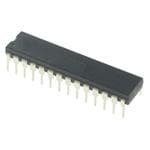
| 描述 | IC DAC 12BIT QUAD V-OUT 28DIP数模转换器- DAC Quad 12-Bit Vout w/ Readback |
| 产品分类 | |
| 品牌 | Analog Devices |
| 产品手册 | |
| 产品图片 |
|
| rohs | 符合RoHS无铅 / 符合限制有害物质指令(RoHS)规范要求 |
| 产品系列 | 数据转换器IC,数模转换器- DAC,Analog Devices DAC8412EPZ- |
| 数据手册 | |
| 产品型号 | DAC8412EPZ |
| PCN其它 | |
| 产品培训模块 | http://www.digikey.cn/PTM/IndividualPTM.page?site=cn&lang=zhs&ptm=19145http://www.digikey.cn/PTM/IndividualPTM.page?site=cn&lang=zhs&ptm=18614http://www.digikey.cn/PTM/IndividualPTM.page?site=cn&lang=zhs&ptm=26125http://www.digikey.cn/PTM/IndividualPTM.page?site=cn&lang=zhs&ptm=26140http://www.digikey.cn/PTM/IndividualPTM.page?site=cn&lang=zhs&ptm=26150http://www.digikey.cn/PTM/IndividualPTM.page?site=cn&lang=zhs&ptm=26147 |
| 产品种类 | 数模转换器- DAC |
| 位数 | 12 |
| 供应商器件封装 | 28-PDIP |
| 分辨率 | 12 bit |
| 包装 | 管件 |
| 商标 | Analog Devices |
| 安装类型 | 通孔 |
| 封装 | Tube |
| 封装/外壳 | 28-DIP(0.600",15.24mm) |
| 封装/箱体 | PDIP-28 |
| 工作温度 | -40°C ~ 85°C |
| 工厂包装数量 | 13 |
| 建立时间 | 6µs |
| 接口类型 | Parallel |
| 数据接口 | 并联 |
| 最大工作温度 | + 85 C |
| 最小工作温度 | - 40 C |
| 标准包装 | 13 |
| 电压参考 | External |
| 电压源 | 单电源 |
| 电源电压-最大 | 5.25 V |
| 电源电压-最小 | 4.75 V |
| 积分非线性 | +/- 2 LSB |
| 稳定时间 | 10 us |
| 系列 | DAC8412 |
| 结构 | R-2R |
| 转换器数 | 4 |
| 转换器数量 | 4 |
| 输出数和类型 | 4 电压,单极4 电压,双极 |
| 输出类型 | Voltage |
| 采样比 | 167 Ksps |
| 采样率(每秒) | 167k |


PDF Datasheet 数据手册内容提取
Quad, 12-Bit DAC Voltage Output with Readback Data Sheet DAC8412/DAC8413 FEATURES FUNCTIONAL BLOCK DIAGRAM +5 V to ±15 V operation VLOGIC VDD VREFH Unipolar or bipolar operation 12 DATA I/O INPUT OUTPUT True voltage output I/O PORT REG A REG A DAC A VOUTA Double-buffered inputs DGND Reset to minimum (DAC8413) or center scale (DAC8412) RINEPGU TB ORUETGP UBT DAC B VOUTB A0 Fast bus access time Readback RA/W1 COLNOTGRICOL RINEPGU TC ORUETGP UCT DAC C VOUTC CS RINEPGU TD ORUETGP UDT DAC D VOUTD APPLICATIONS RESET DAuigtiotmallayt icco tnetsrto ellqeudi pcamliebnrta t ion LDAC VREFL VSS 00274-001 Servo controls Figure 1. Process control equipment GENERAL DESCRIPTION The DAC8412/DAC8413 are quad, 12-bit voltage output They can be operated from a wide variety of supply and reference DACs with readback capability. Built using a complementary voltages with supplies ranging from single +5 V to ±15 V, and BiCMOS process, these monolithic DACs offer the user very references from +2.5 V to ±10 V. Power dissipation is less than high package density. 330 mW with ±15 V supplies and only 60 mW with a +5 V supply. Output voltage swing is set by the two reference inputs V For MIL-STD-883 applications, contact your local Analog REFH and V . By setting the V input to 0 V and V to a Devices, Inc. sales office for the DAC8412/DAC8413/883 data REFL REFL REFH positive voltage, the DAC provides a unipolar positive output sheet, which specifies operation over the −55°C to +125°C range. A similar configuration with V at 0 V and V at a temperature range. All 883 parts are also available on Standard REFH REFL negative voltage provides a unipolar negative output range. Military Drawings 5962-91 76401MXA through 76404M3A. Bipolar outputs are configured by connecting both VREFH and 0.500 V to nonzero voltages. This method of setting output voltage REFL 0.375 +125°C range has advantages over other bipolar offsetting methods +25°C because it is not dependent on internal and external resistors B) 0.250 S with different temperature coefficients. L R ( 0.125 O Digital controls allow the user to load or read back data from any R R E 0 DAC, load any DAC, and transfer data to all DACs at one time. Y T –55°C An active low RESET loads all DAC output registers to midscale ARI–0.125 E for the DAC8412 and zero scale for the DAC8413. LIN–0.250 VVDSSD == –+1155VV The DAC8412/DAC8413 are available in 28-lead plastic DIP, VREFH = +10V –0.375 VREFL = –10V 28-lead ceramic DIP, 28-lead PLCC, and 28-lead LCC packages. TA = –55°C, +25°C, +125°C –0.5000 512 10D24IGIT1A5L3 6INPU2T0 4C6ODE2 5(D48ecim2a5l)60 3072 4096 00274-002 Figure 2. INL vs. Code Over Temperature Rev. G Document Feedback Information furnished by Analog Devices is believed to be accurate and reliable. However, no responsibility is assumed by Analog Devices for its use, nor for any infringements of patents or other One Technology Way, P.O. Box 9106, Norwood, MA 02062-9106, U.S.A. rights of third parties that may result from its use. Specifications subject to change without notice. No license is granted by implication or otherwise under any patent or patent rights of Analog Devices. Tel: 781.329.4700 ©2000–2013 Analog Devices, Inc. All rights reserved. Trademarks and registered trademarks are the property of their respective owners. Technical Support www.analog.com
DAC8412/DAC8413 Data Sheet TABLE OF CONTENTS Features .............................................................................................. 1 Introduction ................................................................................ 14 Applications ....................................................................................... 1 DACs ............................................................................................ 14 Functional Block Diagram .............................................................. 1 Glitch ............................................................................................ 14 General Description ......................................................................... 1 Reference Inputs ......................................................................... 14 aRevision History ............................................................................. 2 Digital I/O ................................................................................... 14 Specifications ..................................................................................... 3 Coding ......................................................................................... 14 Electrical Characteristics ............................................................. 3 Supplies ........................................................................................ 15 Absolute Maximum Ratings ............................................................ 7 Amplifiers .................................................................................... 15 Thermal Resistance ...................................................................... 7 Reference Configurations .......................................................... 16 ESD Caution .................................................................................. 7 Single +5 V Supply Operation .................................................. 17 Pin Configuration and Function Descriptions ............................. 8 Outline Dimensions ....................................................................... 18 Typical Performance Characteristics ............................................. 9 Ordering Guide .......................................................................... 20 Theory of Operation ...................................................................... 14 REVISION HISTORY 4/13—Rev. F to Rev. G Changed Reference Low Input Current from 0 mA (min), 2 mA (typ), 2.75 mA (max) to −2.75 mA (min), −2 mA (typ), 0 mA (max); Table 1 ......................................................................... 3 Changes to Reference Configurations Section ........................... 17 9/09—Rev. E to Rev. F Updated Figure Numbering .............................................. Universal Removed Figure 7 ............................................................................. 6 Changes to Ordering Guide .......................................................... 20 6/07—Rev. D to Rev. E Updated Format .................................................................. Universal Added CERDIP Package .................................................... Universal Changes to Specifications Section .................................................. 3 Changes to Absolute Maximum Ratings Section ......................... 7 Updated Outline Dimensions ....................................................... 18 Changes to Ordering Guide .......................................................... 20 3/00—Rev. C to Rev. D Rev. G | Page 2 of 20
Data Sheet DAC8412/DAC8413 SPECIFICATIONS ELECTRICAL CHARACTERISTICS V = +15.0 V, V = −15.0 V, V = +5.0 V, V = +10.0 V, V = −10.0 V,−40°C ≤ T ≤ +85°C, unless otherwise noted.1 DD SS LOGIC REFH REFL A Table 1. Parameter Symbol Conditions Min Typ Max Unit ACCURACY Integral Nonlinearity Error INL E grade ±0.25 ±0.5 LSB F grade ±1 LSB Differential Nonlinearity Error DNL Monotonic over temperature −1 LSB Min-Scale Error V R = 2 kΩ ±2 LSB ZSE L Full-Scale Error V R = 2 kΩ ±2 LSB FSE L Min-Scale Temperature Coefficient TCV R = 2 kΩ 15 ppm/°C ZSE L Full-Scale Temperature Coefficient TCV R = 2 kΩ 20 ppm/°C FSE L Linearity Matching Adjacent DAC Matching ±1 LSB REFERENCE Positive Reference Input Voltage Range2 V + 2.5 V − 2.5 V REFL DD Negative Reference Input Voltage Range2 −10 V − 2.5 V REFH Reference High Input Current I −2.75 +1.5 +2.75 mA REFH Reference Low Input Current I −2.75 −2 0 mA REFL Large Signal Bandwidth BW −3 dB, V = 0 V to 10 V p-p 160 kHz REFH AMPLIFIER CHARACTERISTICS Output Current I R = 2 kΩ, C = 100 pF –5 +5 mA OUT L L Settling Time t To 0.01%, 10 V step, R = 1 kΩ 10 μs S L Slew Rate SR 10% to 90% 2.2 V/μs Analog Crosstalk 72 dB LOGIC CHARACTERISTICS Logic Input High Voltage V T = 25°C 2.4 V INH A Logic Input Low Voltage V T = 25°C 0.8 V INL A Logic Output High Voltage V I = 0.4 mA 2.4 V OH OH Logic Output Low Voltage V I = −1.6 mA 0.4 V OL OL Logic Input Current I 1 μA IN Input Capacitance C 8 pF IN Digital Feedthrough3 V = 2.5 V, V = 0 V 5 nV-sec REFH REFL LOGIC TIMING CHARACTERISTICS3, 4 Chip Select Write Pulse Width t 80 ns WCS Write Setup t t = 80 ns 0 ns WS WCS Write Hold t t = 80 ns 0 ns WH WCS Address Setup t 0 ns AS Address Hold t 0 ns AH Load Setup t 70 ns LS Load Hold t 30 ns LH Write Data Setup t t = 80 ns 20 ns WDS WCS Write Data Hold t t = 80 ns 0 ns WDH WCS Load Data Pulse Width t 170 ns LDW Reset Pulse Width t 140 ns RESET Chip Select Read Pulse Width t 130 ns RCS Read Data Hold t t = 130 ns 0 ns RDH RCS Read Data Setup t t = 130 ns 0 ns RDS RCS Data to High-Z t C = 10 pF 200 ns DZ L Chip Select to Data t C = 100 pF 160 ns CSD L Rev. G | Page 3 of 20
DAC8412/DAC8413 Data Sheet Parameter Symbol Conditions Min Typ Max Unit SUPPLY CHARACTERISTICS Power Supply Sensitivity PSS 14.25 V ≤ V ≤ 15.75 V 150 ppm/V DD Positive Supply Current I V = 2.5 V 8.5 12 mA DD REFH Negative Supply Current I −10 −6.5 mA SS Power Dissipation P 330 mW DISS 1 All supplies can be varied ±5%, and operation is guaranteed. Device is tested with nominal supplies. 2 Operation is guaranteed over this reference range, but linearity is neither tested nor guaranteed. 3 All parameters are guaranteed by design. 4 All input control signals are specified with tr = tf = 5 ns (10% to 90% of 5 V) and timed from a voltage level of 1.6 V. V = V = +5.0 V ± 5%, V = 0.0 V, V = +2.5 V, V = 0.0 V, V = –5.0 V ± 5%, V = −2.5 V, −40°C ≤ T ≤ +85°C, DD LOGIC SS REFH REFL SS REFL A unless otherwise noted.1 Table 2. Parameter Symbol Conditions Min Typ Max Units ACCURACY Integral Nonlinearity Error INL E grade ±0.5 ±1 LSB F grade ±2 LSB V = 0.0 V, E grade2 ±2 LSB SS V = 0.0 V, F grade2 ±4 LSB SS Differential Nonlinearity Error DNL Monotonic over temperature –1 LSB Min-Scale Error V V = −5.0 V ±4 LSB ZSE SS Full-Scale Error V V = −5.0 V ±4 LSB FSE SS Min-Scale Error V V = 0.0 V ±8 LSB ZSE SS Full-Scale Error V V = 0.0 V ±8 LSB FSE SS Min-Scale Temperature Coefficient TCV 100 ppm/°C ZSE Full-Scale Temperature Coefficient TCV 100 ppm/°C FSE Linearity Matching Adjacent DAC matching ±1 LSB REFERENCE Positive Reference Input Voltage Range3 V + 2.5 V − 2.5 V REFL DD Negative Reference Input Voltage Range V = 0.0 V 0 V − 2.5 V SS REFH V = −5.0 V –2.5 V − 2.5 V SS REFH Reference High Input Current I Code 0x000 –1.0 +1.0 mA REFH Large Signal Bandwidth BW −3 dB, V = 0 V to 2.5 V p-p 450 kHz REFH AMPLIFIER CHARACTERISTICS Output Current I R = 2 kΩ, C = 100 pF –1.25 +1.25 mA OUT L L Settling Time t To 0.01%, 2.5 V step, R = 1 kΩ 7 μs S L Slew Rate SR 10% to 90% 2.2 V/μs LOGIC CHARACTERISTICS Logic Input High Voltage V T = 25°C 2.4 V INH A Logic Input Low Voltage V T = 25°C 0.8 V INL A Logic Output High Voltage V I = 0.4 mA 2.4 V OH OH Logic Output Low Voltage V I = −1.6 mA 0.45 V OL OL Logic Input Current I 1 μA IN Input Capacitance C 8 pF IN LOGIC TIMING CHARACTERISTICS4, 5 Chip Select Write Pulse Width t 150 ns WCS Write Setup t t = 150 ns 0 ns WS WCS Write Hold t t = 150 ns 0 ns WH WCS Address Setup t 0 ns AS Address Hold t 0 ns AH Load Setup t 70 ns LS Load Hold t 50 ns LH Rev. G | Page 4 of 20
Data Sheet DAC8412/DAC8413 Parameter Symbol Conditions Min Typ Max Units Write Data Setup t t = 150 ns 20 ns WDS WCS Write Data Hold t t = 150 ns 0 ns WDH WCS Load Data Pulse Width t 180 ns LDW Reset Pulse Width t 150 ns RESET Chip Select Read Pulse Width t 170 ns RCS Read Data Hold t t = 170 ns 20 ns RDH RCS Read Data Setup t t = 170 ns 0 ns RDS RCS Data to High-Z t C = 10 pF 200 ns DZ L Chip Select to Data t C = 100 pF 320 ns CSD L SUPPLY CHARACTERISTICS Power Supply Sensitivity PSS 100 ppm/V Positive Supply Current I 7 12 mA DD Negative Supply Current I V = −5.0 V −10 mA SS SS Power Dissipation P V = 0 V 60 mW DISS SS V = −5.0 V 110 mW SS 1 All supplies can be varied ±5%, and operation is guaranteed. Device is tested with VDD = 4.75 V. 2 For single-supply operation only (VREFL = 0.0 V, VSS = 0.0 V). Due to internal offset errors, INL and DNL are measured beginning at 0x005. 3 Operation is guaranteed over this reference range, but linearity is neither tested nor guaranteed. 4 All parameters are guaranteed by design. 5 All input control signals are specified with tr = tf = 5 ns (10% to 90% of 5 V) and timed from a voltage level of 1.6 V. tWCS CS tWS tWH R/W tAS tAH tRDS A0/A1 CS tRCS tRDH tLS tLH tLDW R/W LDAC tAS tAH tWDS tWDH A0/A1 DATA IN tDZ DOATUAT HItGCHSD-Z DATA VALID HIGH-Z 00274-003 RESET tRESET 00274-004 Figure 3. Data Output (Read Timing) Figure 4. Data Write (Input and Output Registers) Timing Rev. G | Page 5 of 20
DAC8412/DAC8413 Data Sheet 80ns 80ns CS CS tWS tWH tWS tWH R/W R/W tAS tAS ADDRESS ADODRNEESS ADTDWREOSS ADTHDRREEESS ADFDORUERSS ADDRESS ADODRNEESS ADTDWREOSS ADTHDRREEESS ADFDORUERSS tLS tLH tLS tLH LDAC LDAC DATA IN DVAATLtAWID1DS DVAATLAID2 DVAATLAID3 DVAATLAID4 tWDH 00274-005 DATAIN DVAATLtWAIDD1S DVAATLAID2 DVAATLAID3 DVAATLAID4 tLDWtWDH 00274-006 Figure 5. Single-Buffer Mode Figure 6. Double-Buffer Mode Rev. G | Page 6 of 20
Data Sheet DAC8412/DAC8413 ABSOLUTE MAXIMUM RATINGS THERMAL RESISTANCE T = +25°C, unless otherwise noted. A θ is specified for the worst-case mounting conditions, that is, a JA Table 3. device in socket. Parameter Rating V to V −0.3 V, +33.0 V Table 4. Thermal Resistance SS DD VSS to VLOGIC −0.3 V, +33.0 V Package Type θJA θJC Unit VLOGIC to DGND −0.3 V, +7.0 V 28-Lead Plastic DIP (PDIP) 48 22 °C/W VSS to VREFL −0.3 V, +VSS − 2.0 V 28-Terminal Ceramic Leadless Chip Carrier (LLC) 70 28 °C/W VREFH to VDD +2.0 V, +33.0 V 28-Lead Plastic Leaded Chip Carrier (PLLC) 63 25 °C/W VREFH to VREFL +2.0 V, VSS − VDD 28-Lead Ceramic Dual In-Line Package (CERDIP) 51 9 °C/W Current into Any V pin ±15 mA SS Digital Input Voltage to DGND −0.3 V, V + 0.3 V LOGIC ESD CAUTION Digital Output Voltage to DGND −0.3 V, +7.0 V Operating Temperature Range EP, FP, FPC −40°C to +85°C AT, BT, BTC −55°C to +125°C Junction Temperature 150°C Storage Temperature Range −65°C to +150°C Power Dissipation Package 1000 mW Lead Temperature JEDEC Industry Standard Soldering J-STD-020 Stresses above those listed under Absolute Maximum Ratings may cause permanent damage to the device. This is a stress rating only; functional operation of the device at these or any other conditions above those indicated in the operational section of this specification is not implied. Exposure to absolute maximum rating conditions for extended periods may affect device reliability. Rev. G | Page 7 of 20
DAC8412/DAC8413 Data Sheet PIN CONFIGURATION AND FUNCTION DESCRIPTIONS VREFH 1 28 VREFL SS OUTA OUTB REFH REFL OUTC OUTD SS OUTA OUTB REFH REFL OUTC OUTD VOUTB 2 27 VOUTC V V V V V V V V V V V V V V VOUTA 3 26 VOUTD 4 3 2 1 28 27 26 4 3 2 1 28 27 26 DGVNSDS 54 DAC8412/ 2254 VVDLODGIC DGND 5 INDENTPFIINE R1 25 VDD DGND 5 25 VDD RESET 6 DAC8413 23 CS RESET 6 24 VLOGIC RESET 6 DAC8412/ 24 VLOGIC LDAC 7 TOP VIEW 22 A0 LDAC 7 DAC8412/ 23 CS LDAC 7 DAC8413 23 CS DB0 (LSB) 8 (Not to Scale) 21 A1 DB0 (LSB) 8 DAC8413 22 A0 DB0 (LSB) 8 TOP VIEW 22 A0 DB1 9 20 R/W DB1 9 TOP VIEW 21 A1 DB1 9 (Not to Scale) 21 A1 DB2 10 19 DB11 (MSB) (Not to Scale) DB2 10 20 R/W DB2 10 20 R/W DB3 11 18 DB10 DB3 11 19 DB11 (MSB) DB4 12 17 DB9 DB3 11 19 DB11 (MSB) DDBB56 1134 1165 DDBB87 00274-008 1DB42 1DB53 1DB64 1DB75 1DB86 1DB97 1DB108 00274-009 1DB42 1DB53 1DB64 1DB75 1DB86 1DB97 1DB108 00274-010 Figure 7. PDIP/CERDIP Figure 8. PLCC Figure 9. LCC Table 5. Pin Function Descriptions Pin Number Mnemonic Description 1 V High-Side DAC Reference Input. REFH 2 V DAC B Output. OUTB 3 V DAC A Output. OUTA 4 V Lower Rail Power Supply. SS 5 DGND Digital Ground. 6 RESET Reset Input and Output Registers to all 0s, Enabled at Active Low. 7 LDAC Load Data to DAC, Enabled at Active Low. 8 DB0 Data Bit 0, LSB. 9 DB1 Data Bit 1. 10 DB2 Data Bit 2. 11 DB3 Data Bit 3. 12 DB4 Data Bit 4. 13 DB5 Data Bit 5. 14 DB6 Data Bit 6. 15 DB7 Data Bit 7. 16 DB8 Data Bit 8. 17 DB9 Data Bit 9. 18 DB10 Data Bit 10. 19 DB11 Data Bit 11, MSB. 20 R/W Active Low to Write Data to DAC. Active high to readback previous data at data bit pins with V connected to 5 V. LOGIC 21 A1 Address Bit 1. 22 A0 Address Bit 0. 23 CS Chip Select, Enabled at Active Low. 24 V Voltage Supply for Readback Function. Can be open circuit if not used. LOGIC 25 V Upper Rail Power Supply. DD 26 V DAC D Output. OUTD 27 V DAC C Output. OUTC 28 V Low-Side DAC Reference Input. REFL Rev. G | Page 8 of 20
Data Sheet DAC8412/DAC8413 TYPICAL PERFORMANCE CHARACTERISTICS R (LSB) 1 VVVTADSRS DE= F = =L2 5–+=°11 C–551VV0V R (LSB) 2 VVTVADSRS DE= F = =L2 505=°VV C0V O O R R 1 R R E E Y Y T T RI 0 RI 0 A A E E N N LI LI M M –1 U U XIM–1 XIM A A M M–2 6 7 8 VREF9H (V) 10 11 12 00274-011 1 VREF2H (V) 3 00274-012 Figure 10. DNL vs. VREFH Figure 13. DNL vs. VREFH B) B) S S L L R ( 1 R (0.3 O O R R R R E E Y Y T T RI 0 RI0.2 A A E E N N M LI VDD = 5V M LI VDD = +15V MAXIMU–1 VVTASRS E= F= L2 50=°V C0V MAXIMU0.1 VVTASRS E= F= L2 5–=°1 C05VV 1 VREF2H (V) 3 00274-014 6 8 VREFH (V) 10 12 00274-013 Figure 11. INL vs. VREFH Figure 14. INL vs.VREFH 0.4 0.3 VDD = +15V X+3σ VSS = –15V 0.2 VREFH = +10V 0.1 B) VREFL = –10V B) S S X L L R ( R ( RO 0 RO–0.1 R R LE E X+3σ LE E X–3σ CA–0.2 CA–0.3 S S L- O- UL X ER VDD = +15V F Z VSS = –15V –0.4 –0.5 VREFH = +10V VREFL = –10V X–3σ –0.60 20T0 = HOURS4 O00F OPERAT6I0O0N AT 125°8C00 1000 00274-015 –0.70 20T0 = HOURS4 O00F OPERAT6I0O0N AT 125°8C00 1000 00274-016 Figure 12. Full-Scale Error vs. Time Accelerated by Burn-in Figure 15. Zero-Scale Error vs. Time Accelerated by Burn-In Rev. G | Page 9 of 20
DAC8412/DAC8413 Data Sheet 0.2 1.00 VDD = +15V VDD = 5V VSS = –15V 0.75 VSS = 0V VREFH = +10V VREFH = 2.5V SB) 0 VREFL = –10V B) 0.50 TA = 25°C OR (L R (LS 0.25 R O R R ALE E–0.2 DAC A TY ER 0 L-SC DAC D DAC B EARI–0.25 FUL–0.4 LIN–0.50 DAC C –0.75 –0.6–75 0TEMPERATURE (°C7)5 150 00274-017 –1.000 512 10D2I4GITA15L3 I6NPU2T0 C48ODE2 (5D6e0cima3l0)72 3584 4096 00274-020 Figure 16. Full-Scale Error vs. Temperature Figure 19. Channel-to-Channel Matching (VSUPPLY = +5 V/GND) 0.2 13 VDD = +15V VDD = +15V VSS = –15V VSS = –15V VREFH = +10V VREFL = –10V B) 0 VREFL = –10V S L R ( 10 O RR DAC A A) LE E–0.2 DAC C (mD A D C DAC D I S O- 7 R DAC B ZE–0.4 –0.6–75 0TEMPERATURE (°C7)5 150 00274-018 47 3 1 VREFH (V)5 9 13 00274-021 Figure 17. Zero-Scale Error vs. Temperature Figure 20. IDD vs. VREFH (All DACs High) 0.37500 0.500 VREFH = 10V 0.26125 VREFL = 0V 0.375 TA = 25°C B) 0.18750 B) 0.250 S S R (L 0.08375 R (L 0.125 O O R R ER 0 ER 0 Y Y ARIT–0.09375 ARIT–0.125 NE NE VDD = +15V LI–0.18750 LI–0.250 VSS = –15V VREFH = +10V –0.23125 –0.375 VREFL = –10V TA = –55°C, +25°C, +125°C –0.375000 512 10D2I4GITA15L3 I6NPU2T0 C48ODE2 (5D6e0cima3l0)72 3584 4096 00274-019 –0.5000 512 10D24IGIT1A5L3 6INPU2T0 4C8ODE2 5(D60ecim3a0l)72 3584 4096 00274-022 Figure 18. Channel-to-Channel Matching (VSUPPLY = ±15 V) Figure 21. INL vs. Code Rev. G | Page 10 of 20
Data Sheet DAC8412/DAC8413 10V 10V 1V/DIV 1V/DIV EA EA VDD = +15V VDD = +15V VSS = –15V VSS = –15V TRIG'D VREFH = +10V TRIG'D VREFH = +10V VREFL = –10V VREFL = –10V TA = 25°C TA = 25°C 0–V580ns 1µs/DIV 9.42µs 00274-026 0–V580ns 1µs/DIV 9.42µs 00274-027 Figure 22. Positive Slew Rate Figure 25. Negative Slew Rate 15.5mV 2.0 VDD = +15V 0 VDD = +15V VSS = –15V INPUT VSS = –15V VREFH = +10V –5V VREFH = +10V 1.5 VREFL = –10V VREFL = –10V TA = 25°C TA = 25°C 2mV/DIV A)1.0 m 5V/DIV (H EF R V0.5 I TRIG'D 0 –4.5m–1V.96µs 2µs/DIV 18.04µs 00274-025 –0.50 511 10D23IGIT1A5L3 5INPU2T0 4C7ODE2 5(D59ecim3a0l)71 3583 4095 00274-023 Figure 23. Settling Time (Negative) Figure 26. IVREFH vs. Code 32.5mV 1.0 VDD = +15V 5V VSS = –15V INPUT 0.8 VREFH = +10V 0 VREFL = –10V TA = 25°C 0.6 5mV/DIV 1 LSB ERROR BAND B) S 5V/DIV L (L 0.4 N I TRIG'D 0.2 VDD = +15V VSS = –15V VREFH = +10V 0 VREFL = –10V –17.5m–V1.96µs 2µs/DIV TA = 25°C 18.04µs 00274-024 –0.20.01 0.1 LOAD RESIS1TANCE (kΩ) 10 100 00274-028 Figure 24. Settling Time (Positive) Figure 27. INL vs. Load Resistance Rev. G | Page 11 of 20
DAC8412/DAC8413 Data Sheet 12 100 VDD = +15V VSS = –15V dB) +PSRR GE (V)108 VVTARR EE=FF HL2 5 ==° C–+1100VV N RATIO ( 80 –PSRR A O E VOLT 6 EJECTI 60 L R +PSRR: ULL-SCA 4 SUPPLY 40 VV–PDSSSD R==R –+:1155VV ±1Vp F ER 20 VDD = +15V 2 W VSS = –15V ±1V PO VREFH = +10V ALL DATA 0 00.01 0.1 LOAD RESIS1TANCE (kΩ) 10 100 00274-029 010 100 FR1EkQUENCY (1H0zk) 100k 1M 00274-032 Figure 28. Output Swing vs. Load Resistance Figure 31. PSRR vs. Frequency 10 VDD = +15V VSS = –15V VREFH = +10V 1 VREFL = –10V 0 V) TA = 25°C µ N (dB)–10 NSITY ( 0.10 GAI–30 E DE S VDD = +15V OI VSS = –15V N –50 VREFH = 0 ±100mV 0.01 VREFL = –10V DATA BITS = +5V 200mV p-p –700 10 100 FRE1QkUENCY10 (kHz) 100k 1M 10M 00274-030 0.0011 10 NOISE FRE1Q00UENCY (Hz) 1k 10k 00274-033 Figure 29. Small Signal Response Figure 32. Noise Density vs. Noise Frequency 10 40 IDD 30 VVDSSD == –+1155VV mA) 6 VVRREEFFHL == –+1100VV +ISC T ( VDD= +15V 20 TA = 25°C EN VSS= –15V DATA = 0x000 RR 2 10 CU mA) PLY (UT 0 UP–2 IO S –10 R E OW ISS –20 P–6 –ISC –30 –10–75 0TEMPERATURE (°C7)5 150 00274-031 –40–25 –20 –15 –10 –5VOU0T (V) 5 10 15 20 25 00274-034 Figure 30. Power Supply Current vs. Temperature Figure 33. IOUT vs. VOUT Rev. G | Page 12 of 20
Data Sheet DAC8412/DAC8413 10µs CH1 MEAN 66.19µV 1V 4µs GLITCH AT DAC OUTPUT 1 2 VDD = +15V VSS = –15V VREFH = +10V 1 VREFL = –10V DEGLITCHER OUTPUT 20µV/DIV M 200µs AT A C =H 215 ° C 12.9mV 00274-035 1V CH2 1.86V 00274-037 Figure 34. Broadband Noise Figure 36. Glitch and Deglitched Results 25 VDD = +15V +ISC 20 VSS = 0V 15 VREFH = +10V VREFL = 0V 10 TA = 25°C DATA = 0x800 A) 5 m (UT 0 O I –5 –10 –15 –ISC –20 –25–6 –4 –2 VOU0T (V) 2 4 6 00274-036 Figure 35. IOUT vs. VOUT Rev. G | Page 13 of 20
DAC8412/DAC8413 Data Sheet THEORY OF OPERATION INTRODUCTION REFERENCE INPUTS The DAC8412/DAC8413 are quad, voltage output, 12-bit parallel All four DACs share common reference high (VREFH) and reference input DACs featuring a 12-bit data bus with readback capability. low (VREFL) inputs. The voltages applied to these reference inputs set the output high and low voltage limits of all four of the DACs. The only differences between the DAC8412/DAC8413 are the Each reference input has voltage restrictions with respect to the reset functions. The DAC8412 resets to midscale (Code 0x800), and the DAC8413 resets to minimum scale (Code 0x000). other reference and to the power supplies. The VREFL can be set at any voltage between V and V − 2.5 V, and V can be set to SS REFH REFH The ability to operate from a single 5 V supply is a unique any value between +V − 2.5 V and V + 2.5 V. Note that DD REFL feature of these DACs. because of these restrictions, the DAC8412 references cannot be Operation of the DAC8412/DAC8413 can be viewed by inverted (that is, V cannot be greater than V ). REFL REFH dividing the system into three separate functional groups: the It is important to note that the DAC8412 V input both sinks REFH digital I/O and logic, the digital-to-analog converters, and the and sources current. In addition, the input current of both V REFH output amplifiers. and V are code-dependent. Many references have limited REFL DACS current-sinking capability and must be buffered with an amplifier to drive V . The V has no such special Each DAC is a voltage switched, high impedance (R = 50 kΩ), REFH REFL requirements. R-2R ladder configuration. Each 2R resistor is driven by a pair of switches that connect the resistor to either VREFH or VREFL. It is recommended that the reference inputs be bypassed with GLITCH 0.2 μF capacitors when operating with ±10 V references. This limits the reference bandwidth. Worst-case glitch occurs at the transition between Half-Scale DIGITAL I/O Digital Code 1000 0000 0000 to half-scale minus 1 LSB, 0111 1111 1111. It can be measured at about 2 V μs (see Figure 36). See Table 6 for the digital control logic truth table. Digital I/O For demanding applications such as waveform generation or consists of a 12-bit bidirectional data bus, two registers select precision instrumentation control, a deglitcher circuit can be inputs, A0 and A1, a R/W input, a RESET input, a chip select (CS), implemented with a standard sample-and-hold circuit (see and a load DAC (LDAC) input. Control of the DACs and bus Figure 37). When CS is enabled by synchronizing the hold direction is determined by these inputs as shown in Table 6. Digital period to be longer than the glitch tradition, the output voltage data bits are labeled with the MSB defined as Data Bit 11 and the can be smoothed with minimum disturbance. A quad LSB as Data Bit 0. All digital pins are TTL/CMOS compatible. sample-and-hold amplifier, SMP04, has been used to illustrate See Figure 38 for a simplified I/O logic diagram. The register the deglitching result (see Figure 36). select inputs A0 and A1 select individual DAC registers A DACOUT (Binary Code 00) through D (Binary Code 11). Decoding of the DACOUT1 registers is enabled by the CS input. When CS is high, no S/H decoding takes place, and neither the writing nor the reading of the input registers is enabled. The loading of the second bank of registers is controlled by the asynchronous LDAC input. By DACOUT taking LDAC low while CS is enabled, all output registers can be updated simultaneously. Note that the t required pulse LDW CS width for updating all DACs is a minimum of 170 ns. The R/W input, when enabled by CS, controls the writing to S/H H S H S and reading from the input register. DACOUT1 00274-038 CBoOthD DINAGC8 412/DAC8413 use binary coding. The output Figure 37. Data Output (Read Timing) voltage can be calculated by (V V )N V V REFH REFL OUT REFL 4096 where N is the digital code in decimal. Rev. G | Page 14 of 20
Data Sheet DAC8412/DAC8413 RESET V is the digital output supply voltage for the readback LOGIC function. It is normally connected to +5 V. This pin is a logic The RESET function can be used either at power-up or at any reference input only. It does not supply current to the device. If time during DAC operation. The RESET function is independent the readback function is not being used, V can be left open- LOGIC of CS. This pin is active low and sets the DAC output registers circuit. While V does not supply current to the DAC8412, it LOGIC to either center code for the DAC8412, or zero code for the does supply currents to the digital outputs when readback is used. DAC8413. The reset-to-center code is most useful when the AMPLIFIERS DAC is configured for bipolar references and an output of 0 V after reset is desired. Unlike many voltage output DACs, the DAC8412 features buffered SUPPLIES voltage outputs. Each output is capable of both sourcing and sinking 5 mA at ±10 V, eliminating the need for external Supplies required are V , V , and V . The V supply can SS DD LOGIC SS amplifiers when driving 500 pF or smaller capacitive load in be set between −15 V and 0 V. V is the positive supply; its DD most applications. These amplifiers are short-circuit protected. operating range is between 5 V and 15 V. Table 6. DAC8412/DAC8413 Logic Table A1 A0 R/W CS RS LDAC Input Register Output Register Mode DAC L L L L H L Write Write Transparent A L H L L H L Write Write Transparent B H L L L H L Write Write Transparent C H H L L H L Write Write Transparent D L L L L H H Write Hold Write input A L H L L H H Write Hold Write input B H L L L H H Write Hold Write input C H H L L H H Write Hold Write input D L L H L H H Read Hold Read input A L H H L H H Read Hold Read input B H L H L H H Read Hold Read input C H H H L H H Read Hold Read input D X X X H H L Hold Update all output registers All X X X H H H Hold Hold Hold All X X X X L X All registers reset to midscale/zero-scale1 All X X X H X All registers latched to midscale/zero-scale1 All 1 DAC8412 resets to midscale, and DAC8413 resets to zero scale. L = logic low; H = logic high; X = don’t care. Input and output registers are transparent when asserted. Rev. G | Page 15 of 20
DAC8412/DAC8413 Data Sheet VREFH VDD VSS RDDACA WRDB0 CS DAC A WRDB1 VOUTA WRDACA WRDB2 WRDB3 A0 RDDACB WRDB4 DAC B VOUTB WRDACB WRDB5 INPUT OUTPUT A1 REGISTER WRDB6REGISTER RDDACC WRDB7 DAC C WRDB8 VOUTC WRDACC R/W WRDB9 RDDACD WRDB10 DAC D WRDB11 VOUTD WRDACD DB11..DB0 VLOGIC VLDREAFCL RESET READOUTBAR READBACKDATAIN_DB11 READBACKDATAIN_DB10 READBACK DATAOUT_DB11 READOUT DGND 00274-039 Figure 38. Simplified I/O Logic Diagram +15V Careful attention to grounding is important for accurate operation of the DAC8412. This is not because the DAC8412 is 39kΩ +15V more sensitive than other 12-bit DACs, but because with four outputs and two references, there is greater potential for ground loops. Because the DAC8412 has no analog ground, the ground 6.2Ω VDD BALANCE VREFH must be specified with respect to the reference. 100kΩ 0.2µF AD688 FOR ±10V DAC8412 REFERENCE CONFIGURATIONS AD588 FOR ±5V OR 0.1µF GAIN DAC8413 //10µF 100kΩ Output voltage ranges can be configured as either unipolar or 6.2Ω bipolar, and within these choices, a wide variety of options VREFL 0.2µF exists. The unipolar configuration can be either positive or VSS negative voltage output, and the bipolar configuration can be 1µF either symmetrical or nonsymmetrical. ±5 OR ±10–V1 O5VPERATION 00274-041 +15V +15V Figure 40. Symmetrical Bipolar Operation + Figure 40 (symmetrical bipolar operation) shows the DAC8412 INPUT OUTPUT OP400 VREFH VDD configured for ±10 V operation. See the AD688 data sheet for a full explanation of reference operation. Adjustments may not be 0.2µF REF10 DAC8412 0.1µF required for many applications since the AD688 is a very high TRIM 10kΩ DACO8R413 //10µF accuracy reference. However, if additional adjustments are VREFL required, adjust the DAC8412 full scale first. Begin by loading VSS the digital full-scale code (0xFFF), and then adjust the gain +10V OPERATION –15V 00274-040 aTdhjuenst, paodtjeunstti tohmee btearl atno caet taadinju as tD tAoC se otu tthpeu ct evnotltearg-esc oafl e9 .o9u97tp6u Vt . voltage to 0.000 V. Figure 39. Unipolar +10 V Operation Rev. G | Page 16 of 20
Data Sheet DAC8412/DAC8413 The 0.2 μF bypass capacitors shown at the reference inputs in Figure 41 shows the DAC8412 configured for –10 V to 0 V Figure 40 should be used whenever ±10 V references are used. operation. A –10 V full-scale output voltage reference is Applications with single references or references to ±5 V may connected directly to V for the reference voltage. REFL not require the 0.2 μF bypassing. The 6.2 Ω resistor in series SINGLE +5 V SUPPLY OPERATION with the output of the reference amplifier keeps the amplifier For operation with a 5 V supply, the reference voltage should be from oscillating with the capacitive load. This 6.2 Ω resistor has set between 1.0 V and 2.5 V for optimum linearity. Figure 42 been found to be large enough to stabilize this circuit. Larger shows a REF43 used to supply a 2.5 V reference voltage. The resistor values are acceptable, provided that the drop across the headroom of the reference and DAC are both sufficient to support resistor does not exceed V . Assuming a minimum V of 0.6 V BE BE a 5 V supply with ±5% tolerance. V and V should be and a maximum current of 2.75 mA, then the resistor should be DD LOGIC connected to the same supply. Separate bypassing to each pin under 200 Ω for the loading of a single DAC8412. should also be used. Using two separate references is not recommended. Having two 5V references can cause different drifts with time and temperature; whereas with a single reference, most drifts track. 10µF 0.01µF Unipolar positive full-scale operation can usually be set with a reference with the correct output voltage. This is preferable to INPUT using a reference and dividing down to the required value. For a OUTPUT VREFH VDD 10 V full-scale output, the circuit can be configured as shown in REF43 TRIM 0.2µF DAC8412 0.1µF Figure 41. In this configuration, the full-scale value is set first by 10kΩ OR //10µF DAC8413 adjusting the 10 kΩ resistor for a full-scale output of 9.9976 V. GND VREFL 10kΩ VSS TRIM VREFH VDD ZERSOIN TGOL 2E. 55VV OSPUEPRPALYTION 00274-043 Figure 42. +5 V Single-Supply Operation GND RVEOFELRTAEGNCEE OUTPUT DAC8412 0.1µF 0.2µF OR //10µF DAC8413 0.01µF VREFL VSS 10µF –15V ZERO TO –10V OPERATION 00274-042 Figure 41. Unipolar –10 V Operation Rev. G | Page 17 of 20
DAC8412/DAC8413 Data Sheet OUTLINE DIMENSIONS 0.300(7.62) 0.100(2.54) 0.075 REF 0.064(1.63) (1.91) 0.020(0.51) REF MIN 19 25 0.028(0.71) 18 26 0.022(0.56) 0.05(1.27) 0.458 00..445482((1111..6233))SQ (11M.6A3X) BOVITETWON 1 28 SQ 0.15(3.81) 0.075(1.91) REF REF 12 4 11 5 0.095(2.41) 0.088(2.24) 0.055(1.40) 0.075(1.90) 0.054(1.37) 0.045(1.14) C(RINEOFNPEATRRREOENNLCLTEIHNEOGSNDELISYM)AEANNRDSEIAORRNOESUNANORDETEDAIN-POIPNFRFCOHINPECRSHI;AMTEEQILUFLOIIVMRAELUTEESNRETDISNIMFDOEERNSSIGIONNS 022106-A Figure 43. 28-Terminal Ceramic Leadless Chip Carrier [LCC] (E-28-1) Dimensions shown in inches and (millimeters) 1.565 (39.75) 1.380 (35.05) 28 15 0.580 (14.73) 0.485 (12.31) 1 14 0.625 (15.88) 0.100 (2.54) 0.600 (15.24) BSC 0.195 (4.95) 0.250 (6.35) 0.015 (0.38) MAX GAUGE 0.125 (3.17) 0.015 PLANE (0.38) 0.200 (5.08) MIN 0.115 (2.92) SEATING 0.015 (0.38) PLANE 0.008 (0.20) 0.700 (17.78) 0.022 (0.56) 0.005 (0.13) MAX 0.014 (0.36) MIN 0.070 (1.78) 0.050 (1.27) COMPLIANTTO JEDEC STANDARDS MS-011 CONTROLLING DIMENSIONSARE IN INCHES; MILLIMETER DIMENSIONS (RCINOEFRPEANRREERENN LCTEEHA EODSNSEL MSY)AAAYNR BDEE AR CROOEU NNNFODIGETUDAR-POEPFDRFOA INSPC RWHIAH ETOEQL UFEIO VLRAE LAUEDSNSET. ISN FDOERSIGN. 071006-A Figure 44. 28-Lead Plastic Dual In-Line Package [PDIP] Wide Body (N-28-2) Dimensions shown in inches and (millimeters) Rev. G | Page 18 of 20
Data Sheet DAC8412/DAC8413 0.180 (4.57) 0.048 (1.22) 0.165 (4.19) 0.042 (1.07) 0.056 (1.42) 0.020 (0.51) 0.042 (1.07) MIN 4 26 0.048 (1.22) 5 PIN 1 25 0.021 (0.53) 0.042 (1.07) IDENTIFIER 0.013 (0.33) BOTTOM TOP VIEW 0.050 0.430 (10.92) VIEW (PINS DOWN) (1.27) 0.390 (9.91) (PINS UP) BSC 0.032 (0.81) 0.026 (0.66) 11 19 12 18 0.045 (1.14) 00..445560 ((1111..548320))SQ 0.120 (3.04) 0.025 (0.64) R 0.090 (2.29) 0.495 (12.57) SQ 0.485 (12.32) COMPLIANT TO JEDEC STANDARDS MO-047-AB C(RINOE FNPETARRREOENLNCLTEIHN EOGSN DELISYM) EAANNRSDEI OARNROSEU ANNRDOEET D IAN-OP IPFNRFC OHINPECRSHI;A METQIELU LFIIOVMAREL TUEESNRET DSINI MF DOEENRSSIGIONN.S 042508-A Figure 45. 28-Lead Plastic Leaded Chip Carrier [PLCC] (P-28) Dimensions shown in inches and (millimeters) 0.005 (0.13) 0.100 (2.54) MIN MAX 28 15 0.610 (15.49) 0.500 (12.70) 1 14 PIN 1 0.620 (15.75) 0.225(5.72) 1.490 (37.85) MAX 0.015 (0.38) 0.590 (14.99) MAX MIN 0.150 (3.81) MIN 0.018 (0.46) 0.200 (5.08) 15° 0.008 (0.20) 0.125 (3.18) 0.100 0.070 (1.78) SEATING 0° 0.026 (0.66) (2.54) 0.030 (0.76) PLANE BSC 0.014 (0.36) CONTROLLING DIMENSIONSARE IN INCHES; MILLIMETER DIMENSIONS A (RINEFPEARREENNCTEH EOSNELSY)AANRDE ARROEU NNODETDA-POPFRFO INPCRHIA ETEQ UFIOVRA LUESNET ISN FDOERSIGN. 030106- Figure 46. 28-Lead Ceramic Dual In-Line Package [CERDIP] (Q-28-2) Dimensions shown in inches and (millimeters) Rev. G | Page 19 of 20
DAC8412/DAC8413 Data Sheet ORDERING GUIDE Model1 Notes Temperature Range INL Package Description Package Option DAC8412AT/883C −55°C to +125°C ±0.75 28-Lead Ceramic Dual In-Line Package [CERDIP] Q-28-2 DAC8412BT/883C −55°C to +125°C ±1.5 28-Lead Ceramic Dual In-Line Package [CERDIP] Q-28-2 DAC8412BTC/883C −55°C to +125°C ±1.5 28-Terminal Ceramic Leadless Chip Carrier [LCC] E-28-1 DAC8412EP 2 −40°C to +85°C ±0.5 28-Lead Plastic Dual In-Line Package [PDIP] N-28-2 DAC8412EPZ 2 −40°C to +85°C ±0.5 28-Lead Plastic Dual In-Line Package [PDIP] N-28-2 DAC8412FP 2 −40°C to +85°C ±1 28-Lead Plastic Dual In-Line Package [PDIP] N-28-2 DAC8412FPC 2 −40°C to +85°C ±1 28-Lead Plastic Leaded Chip Carrier [PLCC] P-28 DAC8412FPC-REEL 2 −40°C to +85°C ±1 28-Lead Plastic Leaded Chip Carrier [PLCC] P-28 DAC8412FPCZ 2 −40°C to +85°C ±1 28-Lead Plastic Leaded Chip Carrier [PLCC] P-28 DAC8412FPCZ-REEL 2 −40°C to +85°C ±1 28-Lead Plastic Leaded Chip Carrier [PLCC] P-28 DAC8412FPZ 2 −40°C to +85°C ±1 28-Lead Plastic Dual In-Line Package [PDIP] N-28-2 DAC8413AT/883C −55°C to +125°C ±0.75 28-Lead Ceramic Dual In-Line Package [CERDIP] Q-28-2 DAC8413BT/883C −55°C to +125°C ±1.5 28-Lead Ceramic Dual In-Line Package [CERDIP] Q-28-2 DAC8413BTC/883C −55°C to +125°C ±1.5 28-Terminal Ceramic Leadless Chip Carrier [LCC] E-28-1 DAC8413EP 2 −40°C to +85°C ±0.5 28-Lead Plastic Dual In-Line Package [PDIP] N-28-2 DAC8413EPZ 2 −40°C to +85°C ±0.5 28-Lead Plastic Dual In-Line Package [PDIP] N-28-2 DAC8413FP 2 −40°C to +85°C ±1 28-Lead Plastic Dual In-Line Package [PDIP] N-28-2 DAC8413FPC 2 −40°C to +85°C ±1 28-Lead Plastic Leaded Chip Carrier [PLCC] P-28 DAC8413FPC-REEL 2 −40°C to +85°C ±1 28-Lead Plastic Leaded Chip Carrier [PLCC] P-28 DAC8413FPCZ 2 −40°C to +85°C ±1 28-Lead Plastic Leaded Chip Carrier [PLCC] P-28 DAC8413FPC-REEL 2 −40°C to +85°C ±1 28-Lead Plastic Dual In-Line Package [PDIP] N-28-2 DAC8413FPZ 2 −40°C to +85°C ±1 28-Lead Plastic Dual In-Line Package [PDIP] N-28-2 1 Z = RoHS Compliant Part. 2 If burn-in is required, these models are available in CERDIP. Contact sales. ©2000–2013 Analog Devices, Inc. All rights reserved. Trademarks and registered trademarks are the property of their respective owners. D00274-0-4/13(G) Rev. G | Page 20 of 20
Mouser Electronics Authorized Distributor Click to View Pricing, Inventory, Delivery & Lifecycle Information: A nalog Devices Inc.: DAC8413AT/883C 5962-9176402MXA DAC8412FPCZ DAC8413FP DAC8412EP DAC8413FPCZ 5962- 9176404MXA DAC8412BTC/883C DAC8413FPZ DAC8413FPC DAC8413EP DAC8412BT/883C 5962- 9176404M3A 5962-9176402M3A DAC8412FPC DAC8412FPCZ-REEL DAC8412FP DAC8412EPZ DAC8413FPCZ- REEL DAC8413BT/883C 5962-9176403MXA DAC8413EPZ DAC8413BTC/883C DAC8412FPZ DAC8412AT/883C 5962-9176401MXA