ICGOO在线商城 > DAC8234EVM
 Datasheet下载
- 型号: DAC8234EVM
- 制造商: Texas Instruments
- 库位|库存: xxxx|xxxx
- 要求:
| 数量阶梯 | 香港交货 | 国内含税 |
| +xxxx | $xxxx | ¥xxxx |
查看当月历史价格
查看今年历史价格
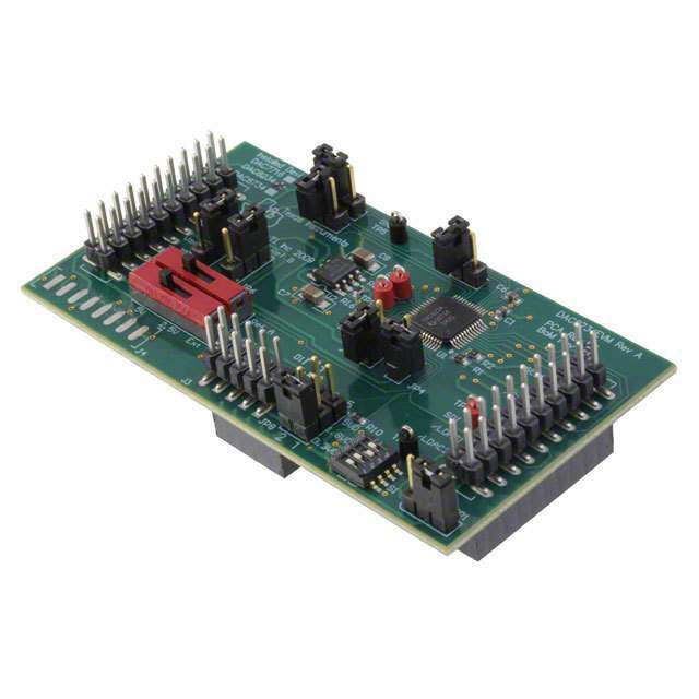
DAC8234EVM产品简介:
ICGOO电子元器件商城为您提供DAC8234EVM由Texas Instruments设计生产,在icgoo商城现货销售,并且可以通过原厂、代理商等渠道进行代购。 提供DAC8234EVM价格参考以及Texas InstrumentsDAC8234EVM封装/规格参数等产品信息。 你可以下载DAC8234EVM参考资料、Datasheet数据手册功能说明书, 资料中有DAC8234EVM详细功能的应用电路图电压和使用方法及教程。
| 参数 | 数值 |
| 产品目录 | 编程器,开发系统嵌入式解决方案 |
| DAC数 | 4 |
| DAC类型 | 电压 |
| 描述 | EVAL MODULE FOR DAC8234数据转换 IC 开发工具 DAC8324 Eval Mod |
| 产品分类 | 评估板 - 数模转换器 (DAC)工程工具 |
| 品牌 | Texas Instruments |
| 产品手册 | |
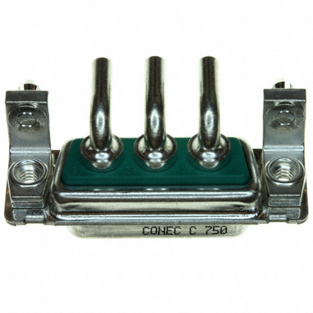
| 产品图片 |
|
| rohs | 否无铅 / 符合限制有害物质指令(RoHS)规范要求 |
| 产品系列 | 模拟与数字IC开发工具,数据转换 IC 开发工具,Texas Instruments DAC8234EVM- |
| 数据手册 | 点击此处下载产品Datasheethttp://www.ti.com/lit/pdf/sbau160 |
| 产品型号 | DAC8234EVM |
| 产品 | Evaluation Boards |
| 产品种类 | 数据转换 IC 开发工具 |
| 位数 | 14 |
| 使用的IC/零件 | DAC8234 |
| 其它名称 | 296-30872 |
| 制造商产品页 | http://www.ti.com/general/docs/suppproductinfo.tsp?distId=10&orderablePartNumber=DAC8234EVM |
| 商标 | Texas Instruments |
| 工作温度 | -40°C ~ 105°C |
| 工作电源电压 | 1.8 V to 5 V |
| 工具用于评估 | DAC8234 |
| 工厂包装数量 | 1 |
| 建立时间 | 8µs |
| 所含物品 | 板 |
| 接口类型 | SPI |
| 数据接口 | SPI |
| 标准包装 | 1 |
| 类型 | DAC |
| 采样率(每秒) | - |


- 商务部:美国ITC正式对集成电路等产品启动337调查
- 曝三星4nm工艺存在良率问题 高通将骁龙8 Gen1或转产台积电
- 太阳诱电将投资9.5亿元在常州建新厂生产MLCC 预计2023年完工
- 英特尔发布欧洲新工厂建设计划 深化IDM 2.0 战略
- 台积电先进制程称霸业界 有大客户加持明年业绩稳了
- 达到5530亿美元!SIA预计今年全球半导体销售额将创下新高
- 英特尔拟将自动驾驶子公司Mobileye上市 估值或超500亿美元
- 三星加码芯片和SET,合并消费电子和移动部门,撤换高东真等 CEO
- 三星电子宣布重大人事变动 还合并消费电子和移动部门
- 海关总署:前11个月进口集成电路产品价值2.52万亿元 增长14.8%


PDF Datasheet 数据手册内容提取
User's Guide SBAU160–October2009 DAC8234EVM DAC8234EVM This user's guide describes the characteristics, operation, and use of the DAC8234EVM. The evaluation module (EVM) is an evaluation board that allows for quick and easy evaluation of the DAC8234. The DAC8234 is a quad, high-accuracy, 14-bit, R-2-R digital-to-analog converter (DAC). The device features low-power operation, good linearity, and the ability to use different reference voltages for the output channels. This EVM allows evaluation of all aspects of the DAC8234. Complete circuit descriptions, schematicdiagrams,andbillofmaterialareincludedinthisdocument. The following related documents are available through the Texas Instruments web site at http://www.ti.com. EVM-CompatibleDeviceDataSheets Device LiteratureNumber DAC8234 SBAS464 REF5025 SBOS410 REF5050 SBOS410 OPA211 SBOS377 TL750L08 SLVS017 Alltrademarksarethepropertyoftheirrespectiveowners. SBAU160–October2009 DAC8234EVM 1 SubmitDocumentationFeedback Copyright©2009,TexasInstrumentsIncorporated
EVMOverview www.ti.com Contents 1 EVMOverview............................................................................................................... 2 2 AnalogInterface ............................................................................................................. 3 3 DigitalInterface .............................................................................................................. 3 4 PowerSupplies .............................................................................................................. 5 5 ReferenceVoltage .......................................................................................................... 5 6 EVMOperation .............................................................................................................. 6 7 SchematicsandLayout .................................................................................................... 8 ListofFigures 1 ReferenceTestPoints...................................................................................................... 6 2 DAC8234EVMDefaultJumperLocations............................................................................... 7 3 DefaultSettingsforSwitchS1(LDACLow) ............................................................................ 8 4 DefaultSettingsforSwitchS2andS3................................................................................... 8 ListofTables 1 J1:AnalogInterfacePinout................................................................................................ 3 2 J2:SerialInterfacePins ................................................................................................... 4 3 J3Configuration:Power-SupplyInput.................................................................................... 5 4 DAC8234EVMBillofMaterials ........................................................................................... 9 1 EVM Overview 1.1 Features DAC8234EVM: • ContainsallsupportcircuitryneededfortheDAC8234 • Voltagereferenceoptions:Either5Vor2.5Vonboard,orexternal • Jumpersonoutputpinsforgainadjustment • CompatiblewiththeTIModularEVMSystem ThismanualcoverstheoperationoftheDAC8234EVM.Throughoutthisdocument,theabbreviationEVM andthetermevaluationmodulearesynonymouswiththeDAC8234EVM. 1.2 Introduction TheDAC8234usesahighspeedSPIinterface(upto50MHz)tocommunicatewithaDSPora microprocessorusingacompatibleserialinterface.TheDACfeaturesfourindividualoutputswhosegain iscontrolledbytheadditionofafeedbackresistor.AnadditionalV pincanrelayanyofthefouroutput MON channelsfromtheDACorthesignalfromtheA pin. IN TheDAC8234EVMisdesignedtoberunineitherbipolar(defaultmode)orunipolarmodesofoperation. Thisflexibledesignallowsforawiderangeofsupplyvoltages.Theoperatingmodecanbecontrolled usinganonboardswitchordigitally,throughthedigitalheader. TheDAC8234EVMisanevaluationmodulebuilttotheTIModularEVMSystemspecification.Itcanbe connectedtoanymodularEVMsysteminterfacecard.TheEVMshipsintheTQFP-48pinpackage option. NotethattheDAC8234EVMhasnomicroprocessorandcannotrunsoftware.Toconnectittoacomputer, sometypeofinterfaceisrequired. Thedeviceshowninthefront-pagefigureistheDAC8734,the16-bitversionoftheDAC8234.The DAC8234isinstalledinplaceoftheDAC8734ontheDAC8234evaluationmodule. 2 DAC8234EVM SBAU160–October2009 SubmitDocumentationFeedback Copyright©2009,TexasInstrumentsIncorporated
www.ti.com AnalogInterface 2 Analog Interface Formaximumflexibility,theDAC8234EVMcaninterfacetomultipleanalogsources.Samtecpartnumbers SSW-110-22-F-D-VS-KandTSM-110-01-T-DV-Pprovidea10-pin,dual-row,headeratJ1.Thisheader providesaccesstotheanaloginputandoutputpinsoftheDAC.ConsultSamtecat http://www.samtec.comorcall1-800-SAMTEC-9foravarietyofmatingconnectoroptions. Table1summarizesthepinoutsforanaloginterfaceJ1. Table1.J1:AnalogInterfacePinout PinNumber Signal Description J1.1 SGND-0 SignalGNDDACoutput0 J1.2 V -0 Analogoutput0 OUT J1.3 SGND-1 SignalGNDDACoutput1 J1.4 V -1 Analogoutput1 OUT J1.5 SGND-2 SignalGNDDACoutput2 J1.6 V -2 Analogoutput2 OUT J1.7 SGND-3 SignalGNDDACoutput3 J1.8 V -3 Analogoutput3 OUT J1.9-13(odd) AGND Analoggroundconnections J1.10 A Auxiliaryanaloginput IN J1.14 V Monitoroutputafterbuffer MON_BUF J1.15 Unused — J1.17-19(odd) AGND Analoggroundconnections J1.18 RefGND Referencegroundpinsonthe DAC8234(seebelow) J1.20 EXTREF+ Externalreferencesourceinput(+ sideofreferenceinput) J1.12 Unused — J1.16 Unused — Theanaloginterfaceispopulatedonthetopoftheevaluationmodel.Thisconfigurationmakesitpossible tostackmultipleEVMstorunthemindaisy-chainmode.J4canbeinstalledwitha90-degreeconnectorto allowaccesstotheanalogoutputsifmultipleEVMsarestacked.TheJ1Bconnectorcanbeinstalledifthe partisusedasastandaloneboard. TheDAC8234canbeconfiguredwithanoutputgainof2or4.Bydefault,theanalogoutputsofthe DAC8234EVMareconfiguredwithagainof4.Ifagainof2isdesired,theproperjumpermustbe installed(JP2-JP5,dependingontheoutputchannel),andthecommandregistermustbesetaccordingly. TheSGNDpinsoftheDAC8234areconnectedtothegroundoftheevaluationboard. TheAuxiliaryAnalogInputpincanbefurtherprotectedfromover-voltageandover-drivingconditions.A Schottkydiode(D1)canbeinstalledtoprotecttheDAC8234fromaninputover-voltagecondition.Anop ampbufferisplacedontheV outputtolimitthecurrentthatpassesthroughthepin. MON TheDAC8234EVMhasanexternalreferencevoltageoption.Ifanexternalreferencevoltageisused, switchesS2andS3mustbeproperlyconfigured.UsetheEXTREF+(J1.20)toapplyanexternal referencevoltage. TheDAC8234isdesignedtohavetheREFGND-AandREFGND-Bpinswithin0.3VoftheAGND. Therefore,werecommendnotusingtheRefGNDpinwhenconnectinganexternalreference.Connectthe groundsourceofthereferencevoltagetothegroundoftheboard(J1.19).SeetheReferenceVoltage sectionformoreinformation. 3 Digital Interface TheDAC8234EVMisaserialinputdataconverter.Theevaluationmoduleisdesignedforinterfacingto multiplecontrolplatforms. SBAU160–October2009 DAC8234EVM 3 SubmitDocumentationFeedback Copyright©2009,TexasInstrumentsIncorporated
DigitalInterface www.ti.com 3.1 Serial Data Interface SamtecpartnumbersSSW-110-22-F-D-VS-KandTSM-110-01-T-DV-Pprovidea10-pin,dual-row, header/socketcombinationatJ2.Thisheader/socketprovidesaccesstothedigitalcontrolandserialdata pinsfrombothJ2A(topside)andJ2B(bottomside)oftheconnector.ConsultSamtecat http://www.samtec.comorcall1-800-SAMTEC-9foravarietyofmatingconnectoroptions. Table2describestheserialinterfacepins. Table2.J2:SerialInterfacePins(1) PinNo. SignalName I/OType Pullup Function J2.1 Unused — — J2.2 GPIO-0 In/Out High GPIO-0 J2.3J2.5 SCLK In None DAC8234SPI clock;pinsare shortedtogether J2.4 DGND In/Out None Digitalground J2.6 GPIO-1 In/Out High GPIO-1 J2.7J2.9 CS In None SPIbuschipselect; pinsareshorted together J2.8 Uni/BipA In High Outputmodeselect ofGroupA J2.10 DGND In/Out None Digitalground J2.11 SDO/SDI In/Out None DAC8234SPIdata in/out J2.12 Uni/BipB In High Outputmodeselect ofGroupB J2.13 Unused — — J2.14 RST In High Inputregisterreset J2.15 LDAC In High GPIOsignalto controlLDACfor DACoutputlatch update J2.16 Unused — — J2.17 LDAC In High AlternateGPIO signaltocontrol LDACforDAC outputlatchupdate J2.18 DGND In/Out None Digitalground J2.19 Unused — — J2.20 Unused — — (1) GroupAcontainsV -0andV -1.GroupBcontainsV -2andV -3. OUT OUT OUT OUT TheSCLKsignalandtheCSsignalcaneachbecontrolledbytwodifferentpinsonJ2.PinsJ2.3andJ2.5 havebeenshortedtogether,aswellaspinsJ2.7andJ2.9. PinsJ2.8,J2.12,J2.14,J2.15,andJ2.17haveweakpull-up/pulldownresistors.Theseresistorsprovide defaultsettingsformanyofthecontrolpins.J2.3,J2.5,J2.7,J2.9,J2.11corresponddirectlytoDAC8234 pins.SeetheDAC8234productdatasheetforcompletedetailsonthesepins. ControlsignalstoandfromtheDAC8234canbeaccessedthroughthedigitalinterface,orswitchesand jumpersfounddirectlyontheEVM.The/LDAC,Uni/BipA,Uni/BipB,andRSTsignalsareinitiallypulled highthrough10kΩ resistorsandcanbecontrolledbyswitchS1orthroughJ2. TheloadDAC(LDAC)pinisconnectedviajumperJP1toeithertheJ2.15orJ2.17pin.UpdatingtheDAC registerscanbecompletedintwodifferentways.LDACcaneitherbetiedtoground,inwhichcasethe inputregistersareimmediatelyupdated,orLDACcanbepulledhigh.Therefore,theDACregistersupdate whenLDACistakenlow.SwitchS1.1canbeclosedtoholdtheLDAClow.SeetheDAC8234datasheet formoreinformationonupdatingtheDAC. 4 DAC8234EVM SBAU160–October2009 SubmitDocumentationFeedback Copyright©2009,TexasInstrumentsIncorporated
www.ti.com PowerSupplies 4 Power Supplies SamtecpartnumbersSSW-105-22-F-D-VS-KandTSM-105-01-T-DV-Pprovidea5-pin,dual-row, header/socketcombinationatJ3.Table3liststheconfigurationdetailsforJ3.Thevoltageinputstothe DACcanbeapplieddirectlytothedevice.TheDAC8234requiresmultiplepowersuppliestooperate. AVDD,AVSS,DVDD,andIOVDDarerequiredtoproperlypowertheDAC. Table3.J3Configuration:Power-SupplyInput PinNo. PinName Function Required J3.1 +VA +4.75Vto+24Vanalogsupply Yes J3.2 –VA –18Vto–4.75Vanalogsupply Yes J3.3 +5VA +5Vanalogsupply No J3.4 –5VA –5Vanalogsupply No J3.5 DGND Digitalgroundinput Yes J3.6 AGND Analoggroundinput Yes J3.7 +1.8VD 1.8Vdigitalsupply Optional J3.8 +3.3VD 3.3Vdigitalsupply Optional J3.9 VD1 Notused No J3.10 +5VD +5V Yes TheDigitalandAnaloggroundinputsareshort-circuitedinternallythroughagroundplane. ThedclogicvoltagefortheDAC8234(IOVDD)isselectablebetween+3.3VD,+1.8VD,or+5VDviathe JP8jumper.Thesepower-supplyvoltagesarereferencedtodigitalground. TheDAC8234EVMisdesignedtoworkineitherunipolarandbipolarmode.Eachmoderequiresdifferent power-supplyconnections.ConsulttheDAC8234datasheetfortherestrictionsonthepowersuppliesfor thetwooperatingmodes. 5 Reference Voltage TheDAC8234EVMhastheabilitytousetwodifferentreferencesourcessimultaneouslyfordifferent outputchannels.REFAandREFBcontrolthereferencevoltagesfortheDAC.OutputchannelsV -0and OUT V -1useREFAasareference.REFBisusedasareferenceforoutputchannelsV -2andV -3. OUT OUT OUT TheevaluationmodulehasthreeoptionsforsupplyingreferencevoltagestotheDAC8234.SwitchS3 (REFA)andS2(REFB)canselectthereferencevoltagefromtheREF5050(U5),REF5025(U4)orusean externalreference.TheREF5050supplies5.0Vtothereference.TheREF5025supplies2.5Vtothe reference.ThesereferencevoltagesareadditionallyfilteredthroughanRCfilterbeforeconnectingtothe DAC8234.TheTL751L08isusedtovoltageregulate+VAtoproperlypowertheREF5025andREF5050. Whenusinganexternalreference,makesurethatthegroundterminal(fromtheexternalsource)is connectedtothegroundoftheEVMboard.Thereisabuilt-indiodeintheDAC8234thatdoesnotallow theRefGND-A/RefGND-Btohavemorethana0.3VdifferencefromtheboardAGNDontheDAC.A jumperacrosspins2and3onJP6andJP7connectstheRefGND-AandRefGND-Btothegroundofthe board. SBAU160–October2009 DAC8234EVM 5 SubmitDocumentationFeedback Copyright©2009,TexasInstrumentsIncorporated
EVMOperation www.ti.com NotethatifanexternalreferencevoltageisinputtoJ1.20,itwillbefilteredthroughafirst-order,low-pass RCfilter.Toinputyourownreferencesignalwithoutthisfilter,connectthereferencesignaldirectlytoTP1 orTP2.Figure1showsthereferencetestpointsontheEVM. Figure1.ReferenceTestPoints 6 EVM Operation Thissectionprovidesinformationontheanaloginput,digitalcontrol,andgeneraloperatingconditionsof theDAC8234EVM. 6.1 Analog Output TheDAC8234hasfouranalogoutputsthatareavailablethroughtheJ1headerortheJ4header.TheJ4 headerisdesignedtouse90-degreeSamtecpins(notinstalled)whenmultipleEVMsarestackedtobe usedindaisy-chainmode. JumpersJ5-J8controlthegainoftheindividualoutputchannelsbyconnectingadditionalfeedback resistorstotheinternalopampbuffer.SeetheDAC8234datasheetformoreinformationonsettingthe gain.Eachanalogoutputisabletoswing±16Vinbipolarmodeand0to20Vinunipolarmode. Thesignalground,SGND-N(fortheoutputsignals),areconnectedtoheaderJ1andareshort-circuitedto theboardground.Alloftheoutputsignalsarereferencedtothegroundoftheboard. V isthechannelmonitoroutput.ItcanrelayanyofthefouranalogoutputsignalsortheA signal.The MON IN V signalisbufferedandcurrent-limitedthroughtheOPA227(U2).Bydefault,theV pinisin3-state MON MON mode,causingtheopamptosaturate.Inordertoavoidtheopampsaturatingtoarail,a200kΩ resistoris putinplace.TheresistorservesasaloadfortheopampwhentheV pinisin3-statemode.However, MON asaresult,thereisanerrorof~1%ontheV signalwhenrelayingasignal. MON_BUF 6.2 Digital Control ThedigitalcontrolsignalscanbeapplieddirectlytoJ1(toporbottomside).ThemodularDAC8234EVM canalsobeconnecteddirectlytoaDSPormicrocontrollerinterfaceboard. NospecificevaluationsoftwareisprovidedwiththisEVM;however,variouscodeexamplesareavailable thatshowhowtouseEVMswithavarietyofdigitalsignalprocessorsfromTexasInstruments.Checkthe respectiveproductfoldersorsendane-mailtodataconvapps@list.ti.comforalistingofavailablecode examples.TheEVMGerberfilesarealsoavailableonrequest. 6 DAC8234EVM SBAU160–October2009 SubmitDocumentationFeedback Copyright©2009,TexasInstrumentsIncorporated
www.ti.com EVMOperation 6.3 Default Jumper Settings and Switch Positions Figure2showsthejumpersfoundontheEVMandtherespectivefactorydefaultconditionsforeach. Figure2.DAC8234EVMDefaultJumperLocations JumperJP1controlswhethertheLDACsignaliscontrolledbyJ2.15orJ2.17.Bydefault,theLDACsignal iscontrolledbyJ2.17butcanbechangedusingJP1. JumpersJP2,JP3,JP4,andJP5areusedtocontrolthegainoftheindividualDACchannels.Bydefault, thejumpersareremoved,resultingineachDACchannelhavingagainof4.Thegainoftheoutput channelis2whenthecorrespondingjumperisinplace. JP6andJP7controlthesignalsappliedtoREFGND-AandREFGND-BontheDAC8234.Bydefault,a jumperisplacedacrossJP6.2andJP6.3aswellasJP7.2andJP7.3.ThisjumperconnectsREFGND-A andREFGND-Btothegroundoftheboardwhenanonboardreferenceisused.Whenanexternal referencesourceisused,itisrecommendedthatthisjumperstayinplaceandconfiguretheexternal referencesourcetoshareacommongroundwiththeEVM.SeetheReferenceVoltagesectionformore information. JumperJP8isusedtocontrolthedigitalvoltageforIOVDD.Bydefault,ajumperisinplacetoshort-circuit pinsJP8.1andJP8.2tousea3.3Vdigitalsupply.IfpinsJP8.3andJP8.4areconnected,a1.8Vdigital supplywillbeused.IfpinsJP8.5andJP8.6areconnected,a5VdigitalsupplywillbeusedforIOVDD. JumperJP9isnotinstalled.IftheuserdesirestodisconnectRFB1fromV ,thetracebetweenJP9 OUT1 mustbecut.JP9canthenbeinstalled. SBAU160–October2009 DAC8234EVM 7 SubmitDocumentationFeedback Copyright©2009,TexasInstrumentsIncorporated
SchematicsandLayout www.ti.com SwitchS1allowstheusertopulldownfourcontrolsignalstoground.LDAC,Uni/BipB,RST,andUni/Bip Acanbepulledlowusingtheswitch.Bydefault,switchpositionS1.1isopen,causingLDACtobe connectedtoground.SwitchesS1.2andS1.4areopentoshort-circuitUni/BipAandUni/BipBtoground. ThisconfigurationsetstheDAC8234tobipolarmode(default).Figure3showsthedefaultsettingsfor switchS1. Figure3.DefaultSettingsforSwitchS1(LDACLow) SwitchS2controlsthereferencevoltageselectionforRefB.Whentheswitchisfurthestleft(position1), theonboard5VreferenceisusedfromtheREF5050.Whentheswitchisinthemiddleposition(position 2),theonboard2.5VreferenceisusedfromtheREF5025.Iftheswitchismovedtotheright(position3), RefBissetuptouseanexternalreference.PinsJ1.18(Ref–)andJ1.20(Ref+)areusedtoapplyan externalreferencevoltage. SwitchS3controlsthereferencevoltageselectionforRefA.Theswitchhasthesamefunctionalityas switchS2.Bydefault,switchS2andswitchS3aresettousethe5Vonboardreference,asFigure4 shows. Figure4.DefaultSettingsforSwitchS2andS3 7 Schematics and Layout SchematicsfortheDAC8234EVMareappendedtothisuser'sguide.Thebillofmaterialsisprovidedin Table4. 7.1 Bill of Materials NOTE: AllcomponentsshouldbecompliantwiththeEuropeanUnionRestrictiononUseof HazardousSubstances(RoHS)Directive.Somepartnumbersmaybeeitherleadedor RoHS.VerifythatpurchasedcomponentsareRoHS-compliant.(Formoreinformationabout TI'spositiononRoHScompliance,seetheTIwebsite.) 8 DAC8234EVM SBAU160–October2009 SubmitDocumentationFeedback Copyright©2009,TexasInstrumentsIncorporated
www.ti.com SchematicsandLayout space Table4.DAC8234EVMBillofMaterials(1) ItemNo. Qty RefDes Description Vendor MfrPartNumber 1 1 N/A Printedwiringboard TexasInstruments 6508538 2 6 C1,C6,C10, Capacitorceramic,1.0μF16VX5R TDK C1608X5R1C105K C11,C14,C15 10%0603 3 7 C2,C3,C4, Capacitorceramic10μF25VX5R MuRata GRM31CR61E106KA12L C5,C7,C8, 120610% C9 4 4 C12,C13, Capacitorceramic10μF10V0603 Panasonic ECJ-1VB1A106M C16,C17 X5R20% 5 0 D1 Notinstalled N/A N/A 6 3 JP1,JP6,JP7 Headerstrip,3-pin(1x3) Samtec TSW-103-07-L-S 7 5 JP2,JP3,JP4, Headerstrip,2-pin(1x2) Samtec TSW-102-07-L-S JP5,JP9 8 1 JP8 Headerstrip,6-pin(2x3) Samtec TSW-103-07-L-D 9 2 J1A,J2A 10-pin,dualrow,SMheader(20Pos.) Samtec TSM-110-01-T-DV-P (TopSide) 10 0 J1B Notinstalled N/A N/A (BottomSide) 11 1 J2B 10-pin,dualrow,SMheader(20Pos.) Samtec SSW-110-22-F-D-VS-K (BottomSide) 12 1 J3A 5-pin,dualrow,SMheader(10Pos.) Samtec TSM-105-01-T-DV-P (TopSide) 13 1 J3B(2) 5-pin,dualrow,SMheader(10Pos.) Samtec SSW-105-22-F-D-VS-K (BottomSide) 14 0 J4 Notinstalled N/A N/A 15 5 R1,R2,R3, Resistor33Ω1/10W5%0603SMD Panasonic ERJ-3GEYJ330V R4,R5 16 6 R6,R7,R8, Resistor10kΩ1/10W5%0603SMD Yageo RC0603JR-0710KL R9,R10,R11 17 2 R12,R13 Resistor1.0kΩ1/10W5%0603SMD Panasonic ERJ-3GEYJ102V 18 2 R14,R15 Resistor1.0Ω1/10W5%0603 Panasonic ERJ-3GEYJ1R0V 19 1 R16 Resistor200KOHM1/10W1%0603 Panasonic ERJ-3EKF2003V SMD 20 1 S1 Switchdiptape4pos. C&K TDA04H0SB1R 21 2 S2,S3 SWSlideultraminisp3tTopAct NKK SS14MDP2 22 3 TP1,TP2,TP3 Testpoint-single.025pin,red Keystone 5000 23 2 TP4,TP5 Testpoint-single.025pin,black Keystone 5001 24 1 U1 Quad,14-bit,high-accuracyDAC, TexasInstruments DAC8234SPFB TQFPpackage 25 1 U2 OPA227,differentialoperational TexasInstruments OPA227UA amplifier 26 1 U3 Singleoutput,8Vvoltageregulator TexasInstruments TL750L08CD 27 1 U4 Precisionvoltagereference2.5V TexasInstruments REF5025AID 28 1 U5 Precisionvoltagereference5.0V TexasInstruments REF5050AID 29 8 N/A 0.100Shunt-Black Samtec SNT-100-BK-T (1) Manufacturerandpartnumberforitemsmaybesubstitutedwithelectricallyequivalentitems. (2) J3Bpartsarenotshownintheschematicdiagram.J3BisinstalledonthebottomsideofthePWBoppositetoJ3A. SBAU160–October2009 DAC8234EVM 9 SubmitDocumentationFeedback Copyright©2009,TexasInstrumentsIncorporated
1 2 3 4 5 6 REVISION HISTORY REV ENGINEERING CHANGE NUMBER APPROVED IOVDD +VA -VA +5VD LDAC SDO C3 C4 C6 C1 10uF 10uF 1uF CS 1uF C2 C5 10uF 10uF SCLK D D GPIO-0 1 2 357 468 GUnPiI/OB-i1p A R6 R7 R8 R9 R10R11 13 2635 2833 14 30 29 +VA C7 C3POSJ_PJ1UMPER SerJi2a1357911911111lA 1313579Hea111111112d0240246802468er Top URGGUURSSnnnPPiiiTTII///OOBBB--iii01ppp BAB CSSSLUUGGRCDDDSSnnPPiiLTIOIIA//OOBBKC--ii01pp AB 10k 10k 810k76510kSD11I0PkSW1I0TkRRRRRC12345H-4 333333333332A2K2 D1B414332211470867549222345617 ACSSSLUUNNNNNNNNRIOVDDDCDDiSnnCCCCCCCCSnAiiLIOT//BBKCiiAVDDpp ABAVDD AVSSDAAVSSUC182DVDD34 REF-ASSSSRRRRRRRRGGGGVVVVFFFFFFFFVooooNNNNBBBBBBBBREFGND-AmuuuuDDDD12121212tttto----------------001122330123n0123 3111122224444343445768312046538091 R20106k 23U2-VA74 C108u1OF0PuAF6227JP9 JJJJPPPP2345 11111J13579135791B JD1AAAAAAAAAVAA0123GGGCGGU((((135ONNNNNG----))))DDDMDDHTEA246RRAAAARn-E0123aAEAAAA((((FlF++++No+4567-g))))A tLo OoGn2468111112ly024680 beVVVVAVEE pxxioooomnottuuuuRRopttttn----uEE0123_lFFabt-+uedf at top of board JH4EA12345678DER-8C SerialJ H2Beader111 B579otto112m680 TP3 1234 13A1K1 D1A DGND AGND GPIO-0GPIO-1 REF-B REFGND-B 7911111357 11111024688 SDI 11 27 89 31 32 DAU1G9HT2E0R ANALOG BOTTOM CS -VA SCLK JP7 JP6 and JP7 control the RefGND 3POS_JUMPER +VA TP1 B UTL3750L08 123 NK123CK_SS1C4MDP2 R1k12 J3PP6OS_JUMPER B C109uF 854 INNnCCputComOuCCCtooopmmmut 1236 C1u1F0 243 URE5VGTEFINN5MD0P50VTORUIMT 65 R114 ExStR2EF+ C101u6F TP4 TP5 C14 7 1uF C12 +3.3VD+1.8VD +5VA +VA -VA -5VA +5VD 10uF J3 C1u1F1 243 U4VGTEINNMDPVTORUIMT 65 TP2 13579 ++D++V513GV..A83NAVVDDD A+-GV55-NVVDVDADA1 246810 ti REF5025 R115 R13 DAUGHTER-POWER 1k C15 A 1uF C13 S3 A 10uF NKK_SS14MDP2 C17 PRECISION ANALOG PRODUCTS 10uF HIGH-PERFORMANCE ANALOG DIVISION SEMICONDUCTOR GROUP 246JP8 5411 EAST WILLIAMS BOULEVARD, TUCSON, AZ 85711 USA IOVDD JPR-2X3 ENGINEERT. Calabria TITLE DAC8734EVM DRAWN BYT. Calabria 135 DOCUMENT CONTROL NO.6508538 SIZEB DATE REV A SHEET OF FILE 1 2 3 4 5 6
EvaluationBoard/KitImportantNotice TexasInstruments(TI)providestheenclosedproduct(s)underthefollowingconditions: Thisevaluationboard/kitisintendedforuseforENGINEERINGDEVELOPMENT,DEMONSTRATION,OREVALUATION PURPOSESONLYandisnotconsideredbyTItobeafinishedend-productfitforgeneralconsumeruse.Personshandlingthe product(s)musthaveelectronicstrainingandobservegoodengineeringpracticestandards.Assuch,thegoodsbeingprovidedare notintendedtobecompleteintermsofrequireddesign-,marketing-,and/ormanufacturing-relatedprotectiveconsiderations, includingproductsafetyandenvironmentalmeasurestypicallyfoundinendproductsthatincorporatesuchsemiconductor componentsorcircuitboards.Thisevaluationboard/kitdoesnotfallwithinthescopeoftheEuropeanUniondirectivesregarding electromagneticcompatibility,restrictedsubstances(RoHS),recycling(WEEE),FCC,CEorUL,andthereforemaynotmeetthe technicalrequirementsofthesedirectivesorotherrelateddirectives. Shouldthisevaluationboard/kitnotmeetthespecificationsindicatedintheUser’sGuide,theboard/kitmaybereturnedwithin30 daysfromthedateofdeliveryforafullrefund.THEFOREGOINGWARRANTYISTHEEXCLUSIVEWARRANTYMADEBY SELLERTOBUYERANDISINLIEUOFALLOTHERWARRANTIES,EXPRESSED,IMPLIED,ORSTATUTORY,INCLUDING ANYWARRANTYOFMERCHANTABILITYORFITNESSFORANYPARTICULARPURPOSE. Theuserassumesallresponsibilityandliabilityforproperandsafehandlingofthegoods.Further,theuserindemnifiesTIfromall claimsarisingfromthehandlingoruseofthegoods.Duetotheopenconstructionoftheproduct,itistheuser’sresponsibilityto takeanyandallappropriateprecautionswithregardtoelectrostaticdischarge. EXCEPTTOTHEEXTENTOFTHEINDEMNITYSETFORTHABOVE,NEITHERPARTYSHALLBELIABLETOTHEOTHER FORANYINDIRECT,SPECIAL,INCIDENTAL,ORCONSEQUENTIALDAMAGES. TIcurrentlydealswithavarietyofcustomersforproducts,andthereforeourarrangementwiththeuserisnotexclusive. TIassumesnoliabilityforapplicationsassistance,customerproductdesign,softwareperformance,orinfringementof patentsorservicesdescribedherein. PleasereadtheUser’sGuideand,specifically,theWarningsandRestrictionsnoticeintheUser’sGuidepriortohandlingthe product.Thisnoticecontainsimportantsafetyinformationabouttemperaturesandvoltages.ForadditionalinformationonTI’s environmentaland/orsafetyprograms,pleasecontacttheTIapplicationengineerorvisitwww.ti.com/esh. NolicenseisgrantedunderanypatentrightorotherintellectualpropertyrightofTIcoveringorrelatingtoanymachine,process,or combinationinwhichsuchTIproductsorservicesmightbeorareused. FCCWarning Thisevaluationboard/kitisintendedforuseforENGINEERINGDEVELOPMENT,DEMONSTRATION,OREVALUATION PURPOSESONLYandisnotconsideredbyTItobeafinishedend-productfitforgeneralconsumeruse.Itgenerates,uses,and canradiateradiofrequencyenergyandhasnotbeentestedforcompliancewiththelimitsofcomputingdevicespursuanttopart15 ofFCCrules,whicharedesignedtoprovidereasonableprotectionagainstradiofrequencyinterference.Operationofthis equipmentinotherenvironmentsmaycauseinterferencewithradiocommunications,inwhichcasetheuserathisownexpense willberequiredtotakewhatevermeasuresmayberequiredtocorrectthisinterference. EVMWarningsandRestrictions ItisimportanttooperatethisEVMwithintheinputvoltagerangeof–16.5Vto+21Vandtheoutputvoltagerangeof–15Vto+15V. Exceedingthespecifiedinputrangemaycauseunexpectedoperationand/orirreversibledamagetotheEVM.Ifthereare questionsconcerningtheinputrange,pleasecontactaTIfieldrepresentativepriortoconnectingtheinputpower. Applyingloadsoutsideofthespecifiedoutputrangemayresultinunintendedoperationand/orpossiblepermanentdamagetothe EVM.PleaseconsulttheEVMUser'sGuidepriortoconnectinganyloadtotheEVMoutput.Ifthereisuncertaintyastotheload specification,pleasecontactaTIfieldrepresentative. Duringnormaloperation,somecircuitcomponentsmayhavecasetemperaturesgreaterthan+30°C.TheEVMisdesignedto operateproperlywithcertaincomponentsabove+60°Caslongastheinputandoutputrangesaremaintained.Thesecomponents includebutarenotlimitedtolinearregulators,switchingtransistors,passtransistors,andcurrentsenseresistors.Thesetypesof devicescanbeidentifiedusingtheEVMschematiclocatedintheEVMUser'sGuide.Whenplacingmeasurementprobesnear thesedevicesduringoperation,pleasebeawarethatthesedevicesmaybeverywarmtothetouch. MailingAddress:TexasInstruments,PostOfficeBox655303,Dallas,Texas75265 Copyright©2009,TexasInstrumentsIncorporated
IMPORTANTNOTICE TexasInstrumentsIncorporatedanditssubsidiaries(TI)reservetherighttomakecorrections,modifications,enhancements,improvements, andotherchangestoitsproductsandservicesatanytimeandtodiscontinueanyproductorservicewithoutnotice.Customersshould obtainthelatestrelevantinformationbeforeplacingordersandshouldverifythatsuchinformationiscurrentandcomplete.Allproductsare soldsubjecttoTI’stermsandconditionsofsalesuppliedatthetimeoforderacknowledgment. TIwarrantsperformanceofitshardwareproductstothespecificationsapplicableatthetimeofsaleinaccordancewithTI’sstandard warranty.TestingandotherqualitycontroltechniquesareusedtotheextentTIdeemsnecessarytosupportthiswarranty.Exceptwhere mandatedbygovernmentrequirements,testingofallparametersofeachproductisnotnecessarilyperformed. TIassumesnoliabilityforapplicationsassistanceorcustomerproductdesign.Customersareresponsiblefortheirproductsand applicationsusingTIcomponents.Tominimizetherisksassociatedwithcustomerproductsandapplications,customersshouldprovide adequatedesignandoperatingsafeguards. TIdoesnotwarrantorrepresentthatanylicense,eitherexpressorimplied,isgrantedunderanyTIpatentright,copyright,maskworkright, orotherTIintellectualpropertyrightrelatingtoanycombination,machine,orprocessinwhichTIproductsorservicesareused.Information publishedbyTIregardingthird-partyproductsorservicesdoesnotconstitutealicensefromTItousesuchproductsorservicesora warrantyorendorsementthereof.Useofsuchinformationmayrequirealicensefromathirdpartyunderthepatentsorotherintellectual propertyofthethirdparty,oralicensefromTIunderthepatentsorotherintellectualpropertyofTI. ReproductionofTIinformationinTIdatabooksordatasheetsispermissibleonlyifreproductioniswithoutalterationandisaccompanied byallassociatedwarranties,conditions,limitations,andnotices.Reproductionofthisinformationwithalterationisanunfairanddeceptive businesspractice.TIisnotresponsibleorliableforsuchaltereddocumentation.Informationofthirdpartiesmaybesubjecttoadditional restrictions. ResaleofTIproductsorserviceswithstatementsdifferentfromorbeyondtheparametersstatedbyTIforthatproductorservicevoidsall expressandanyimpliedwarrantiesfortheassociatedTIproductorserviceandisanunfairanddeceptivebusinesspractice.TIisnot responsibleorliableforanysuchstatements. TIproductsarenotauthorizedforuseinsafety-criticalapplications(suchaslifesupport)whereafailureoftheTIproductwouldreasonably beexpectedtocauseseverepersonalinjuryordeath,unlessofficersofthepartieshaveexecutedanagreementspecificallygoverning suchuse.Buyersrepresentthattheyhaveallnecessaryexpertiseinthesafetyandregulatoryramificationsoftheirapplications,and acknowledgeandagreethattheyaresolelyresponsibleforalllegal,regulatoryandsafety-relatedrequirementsconcerningtheirproducts andanyuseofTIproductsinsuchsafety-criticalapplications,notwithstandinganyapplications-relatedinformationorsupportthatmaybe providedbyTI.Further,BuyersmustfullyindemnifyTIanditsrepresentativesagainstanydamagesarisingoutoftheuseofTIproductsin suchsafety-criticalapplications. TIproductsareneitherdesignednorintendedforuseinmilitary/aerospaceapplicationsorenvironmentsunlesstheTIproductsare specificallydesignatedbyTIasmilitary-gradeor"enhancedplastic."OnlyproductsdesignatedbyTIasmilitary-grademeetmilitary specifications.BuyersacknowledgeandagreethatanysuchuseofTIproductswhichTIhasnotdesignatedasmilitary-gradeissolelyat theBuyer'srisk,andthattheyaresolelyresponsibleforcompliancewithalllegalandregulatoryrequirementsinconnectionwithsuchuse. TIproductsareneitherdesignednorintendedforuseinautomotiveapplicationsorenvironmentsunlessthespecificTIproductsare designatedbyTIascompliantwithISO/TS16949requirements.Buyersacknowledgeandagreethat,iftheyuseanynon-designated productsinautomotiveapplications,TIwillnotberesponsibleforanyfailuretomeetsuchrequirements. FollowingareURLswhereyoucanobtaininformationonotherTexasInstrumentsproductsandapplicationsolutions: Products Applications Amplifiers amplifier.ti.com Audio www.ti.com/audio DataConverters dataconverter.ti.com Automotive www.ti.com/automotive DLP®Products www.dlp.com Broadband www.ti.com/broadband DSP dsp.ti.com DigitalControl www.ti.com/digitalcontrol ClocksandTimers www.ti.com/clocks Medical www.ti.com/medical Interface interface.ti.com Military www.ti.com/military Logic logic.ti.com OpticalNetworking www.ti.com/opticalnetwork PowerMgmt power.ti.com Security www.ti.com/security Microcontrollers microcontroller.ti.com Telephony www.ti.com/telephony RFID www.ti-rfid.com Video&Imaging www.ti.com/video RF/IFandZigBee®Solutions www.ti.com/lprf Wireless www.ti.com/wireless MailingAddress:TexasInstruments,PostOfficeBox655303,Dallas,Texas75265 Copyright©2009,TexasInstrumentsIncorporated