ICGOO在线商城 > 集成电路(IC) > 数据采集 - 数模转换器 > DAC101S101CIMM

 Datasheet下载
- 型号: DAC101S101CIMM
- 制造商: Texas Instruments
- 库位|库存: xxxx|xxxx
- 要求:
| 数量阶梯 | 香港交货 | 国内含税 |
| +xxxx | $xxxx | ¥xxxx |
查看当月历史价格
查看今年历史价格
DAC101S101CIMM产品简介:
ICGOO电子元器件商城为您提供DAC101S101CIMM由Texas Instruments设计生产,在icgoo商城现货销售,并且可以通过原厂、代理商等渠道进行代购。 DAC101S101CIMM价格参考。Texas InstrumentsDAC101S101CIMM封装/规格:数据采集 - 数模转换器, 10 位 数模转换器 1 8-VSSOP。您可以下载DAC101S101CIMM参考资料、Datasheet数据手册功能说明书,资料中有DAC101S101CIMM 详细功能的应用电路图电压和使用方法及教程。
| 参数 | 数值 |
| 产品目录 | 集成电路 (IC) |
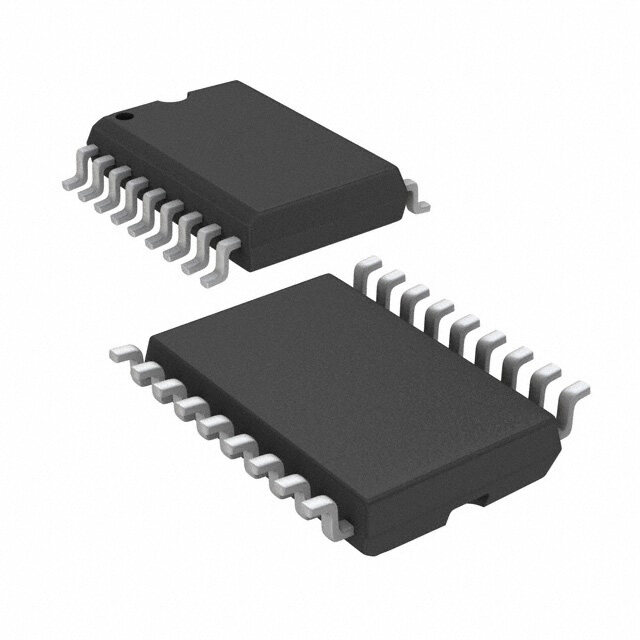
| 描述 | IC CONV D-A 10BIT R-R 8VSSOP |
| 产品分类 | |
| 品牌 | Texas Instruments |
| 数据手册 | |
| 产品图片 |
|
| 产品型号 | DAC101S101CIMM |
| PCN设计/规格 | |
| rohs | 含铅 / 不符合限制有害物质指令(RoHS)规范要求 |
| 产品系列 | - |
| 位数 | 10 |
| 供应商器件封装 | 8-VSSOP |
| 其它名称 | DAC101S101CIMMTR |
| 包装 | 带卷 (TR) |
| 安装类型 | 表面贴装 |
| 封装/外壳 | 8-TSSOP,8-MSOP(0.118",3.00mm 宽) |
| 工作温度 | -40°C ~ 105°C |
| 建立时间 | 5µs |
| 数据接口 | DSP,MICROWIRE™,QSPI™,串行,SPI™ |
| 标准包装 | 1,000 |
| 电压源 | 单电源 |
| 转换器数 | 1 |
| 输出数和类型 | 1 电压,单极1 电压,双极 |
| 采样率(每秒) | - |


- 商务部:美国ITC正式对集成电路等产品启动337调查
- 曝三星4nm工艺存在良率问题 高通将骁龙8 Gen1或转产台积电
- 太阳诱电将投资9.5亿元在常州建新厂生产MLCC 预计2023年完工
- 英特尔发布欧洲新工厂建设计划 深化IDM 2.0 战略
- 台积电先进制程称霸业界 有大客户加持明年业绩稳了
- 达到5530亿美元!SIA预计今年全球半导体销售额将创下新高
- 英特尔拟将自动驾驶子公司Mobileye上市 估值或超500亿美元
- 三星加码芯片和SET,合并消费电子和移动部门,撤换高东真等 CEO
- 三星电子宣布重大人事变动 还合并消费电子和移动部门
- 海关总署:前11个月进口集成电路产品价值2.52万亿元 增长14.8%


PDF Datasheet 数据手册内容提取
Product Sample & Technical Tools & Support & Folder Buy Documents Software Community DAC101S101,DAC101S101-Q1 SNAS321G–JUNE2005–REVISEDAPRIL2016 DAC101S101 and DAC101S101Q-1 10-Bit Micro Power, RRO Digital-to-Analog Converter 1 Features 3 Description • DAC101S101QisAEC-Q100Grade1Qualified The DAC101S101 is a full-featured, general purpose 1 10-bit voltage-output digital-to-analog converter andisManufacturedonanAutomotiveGrade (DAC) that can operate from a single +2.7 V to 5.5 V Flow. supply and consumes just 175 µA of current at 3.6 • EnsuredMonotonicity Volts. The on-chip output amplifier allows rail-to-rail • LowPowerOperation output swing and the three wire serial interface operates at clock rates up to 30 MHz over the • Rail-to-RailVoltageOutput specified supply voltage range and is compatible with • Power-onResettoZeroVoltsOutput standard SPI, QSPI, MICROWIRE and DSP • WideTemperatureRangeof −40°Cto+125°C interfaces. Competitive devices are limited to 20 MHz • WidePowerSupplyRangeof2.7Vto5.5V clock rates at supply voltages in the 2.7 V to 3.6 V range. • SmallPackages • PowerDownFeature The supply voltage for the DAC101S101 serves as its voltage reference, providing the widest possible • Resolution10bits output dynamic range. A power-on reset circuit • DNL+0.15,–0.05LSB(typical) ensures that the DAC output powers up to zero volts • OutputSettlingTime8 μs(typical) and remains there until there is a valid write to the device. A power-down feature reduces power • ZeroCodeError3.3mV(typical) consumptiontolessthanamicroWatt. • Full-ScaleError−0.06%FS(typical) • PowerConsumption DeviceInformation(1) – NormalMode,0.63mW(3.6V)/1.41mW(5.5 PARTNUMBER PACKAGE BODYSIZE(NOM) V)typical DAC101S101 VSSOP(8) 3.00mm×3.00mm – PowerDownMode,0.14 μW(3.6V)/0.33 μW DAC101S101, SOT-23(6) 1.60mm×2.90mm (5.5V)typical DAC101S101-Q1 (1) For all available packages, see the orderable addendum at 2 Applications theendofthedatasheet. • Battery-PoweredInstruments • DigitalGainandOffsetAdjustment • ProgrammableVoltage& CurrentSources • ProgrammableAttenuators • Automotive DNLatV =3V A 1 An IMPORTANT NOTICE at the end of this data sheet addresses availability, warranty, changes, use in safety-critical applications, intellectualpropertymattersandotherimportantdisclaimers.PRODUCTIONDATA.
DAC101S101,DAC101S101-Q1 SNAS321G–JUNE2005–REVISEDAPRIL2016 www.ti.com Table of Contents 1 Features.................................................................. 1 8.4 DeviceFunctionalModes........................................18 2 Applications........................................................... 1 8.5 Programming..........................................................19 3 Description............................................................. 1 9 ApplicationandImplementation........................ 21 4 RevisionHistory..................................................... 2 9.1 ApplicationInformation............................................21 9.2 TypicalApplication..................................................21 5 Description(continued)......................................... 3 10 PowerSupplyRecommendations..................... 23 6 PinConfigurationandFunctions......................... 3 10.1 UsingReferencesasPowerSupplies...................23 7 Specifications......................................................... 4 11 Layout................................................................... 26 7.1 AbsoluteMaximumRatings......................................4 11.1 LayoutGuidelines.................................................26 7.2 ESDRatingsDAC101S101......................................4 11.2 LayoutExample....................................................26 7.3 ESDRatingsDAC101S101-Q1................................4 12 DeviceandDocumentationSupport................. 27 7.4 RecommendedOperatingConditions......................5 7.5 ThermalInformation..................................................5 12.1 DeviceSupport ....................................................27 7.6 ElectricalCharacteristics..........................................6 12.2 RelatedLinks........................................................28 7.7 A.C.andTimingRequirements................................9 12.3 CommunityResources..........................................28 7.8 TypicalCharacteristics............................................11 12.4 Trademarks...........................................................28 12.5 ElectrostaticDischargeCaution............................28 8 DetailedDescription............................................ 17 12.6 Glossary................................................................28 8.1 Overview.................................................................17 13 Mechanical,Packaging,andOrderable 8.2 FunctionalBlockDiagram.......................................17 Information........................................................... 28 8.3 FeatureDescription.................................................17 4 Revision History NOTE:Pagenumbersforpreviousrevisionsmaydifferfrompagenumbersinthecurrentversion. ChangesfromRevisionF(March2013)toRevisionG Page • AddedDeviceInformationtable,ESDRatingstable,FeatureDescriptionsection,DeviceFunctionalModes, ApplicationandImplementationsection,PowerSupplyRecommendationssection,Layoutsection,Deviceand DocumentationSupportsection,andMechanical,Packaging,andOrderableInformationsection....................................... 1 • UpdatedOperatingConditionstabletoaRecommendedOperatingConditionstable.......................................................... 5 • UpdatedLayout,Grounding,andBypassingsectiontoaLayoutGuidelinessection.......................................................... 26 ChangesfromRevisionE(March2013)toRevisionF Page • ChangedlayoutofNationalDataSheettoTIformat........................................................................................................... 26 2 SubmitDocumentationFeedback Copyright©2005–2016,TexasInstrumentsIncorporated ProductFolderLinks:DAC101S101 DAC101S101-Q1
DAC101S101,DAC101S101-Q1 www.ti.com SNAS321G–JUNE2005–REVISEDAPRIL2016 5 Description (continued) The low power consumption and small packages of the DAC101S101 make it an excellent choice for use in batteryoperatedequipment. The DAC101S101 is a direct replacement for the AD5310 and is one of a family of pin compatible DACs, including the 8-bit DAC081S101 and the 12-bit DAC121S101. The DAC101S101 operates over the extended industrialtemperaturerangeof −40°Cto+105°CwhiletheDAC101S101QoperatesovertheGrade1automotive temperature range of −40°C to +125°C. The DAC101S101 is available in a 6-lead SOT and an 8-lead VSSOP andtheDAC101S101Qisavailabeinthe6-leadSOTonly. 6 Pin Configuration and Functions DAC101S101andDAC101S101-Q1DDCPackage 6-Pin(SOT-23) DAC101S101DGKPackage TopView 8-Pin(VSSOP) TopView VO UT 1 6 SYNC VA 1 8 GND GND 2 5 SCLK NC 2 7 D IN VA 3 4 DIN NC 3 6 SCLK VOUT 4 5 SYNC PinFunctions PIN DAC101S101 DAC101S101-Q1 I/O(1) DESCRIPTION NAME SOT-23 VSSOP SOT-23 SerialDataInput.Dataisclockedintothe16-bitshiftregisteronthe D 4 7 4 I IN fallingedgesofSCLKafterthefallofSYNC. GND 2 8 2 G Groundreferenceforallon-chipcircuitry. NC – 2,3 – – NoConnect.Thereisnointernalconnectiontothesepins. SerialClockInput.Dataisclockedintotheinputshiftregisteronthe SCLK 5 6 5 I fallingedgesofthispin. Framesynchronizationinputforthedatainput.Whenthispingoeslow,it enablestheinputshiftregisteranddataistransferredonthefalling edgesofSCLK.TheDACisupdatedonthe16thclockcycleunless SYNC 6 5 6 I SYNCisbroughthighbeforethe16thclock,inwhichcasetherising edgeofSYNCactsasaninterruptandthewritesequenceisignoredby theDAC. V 3 1 3 S PowersupplyandReferenceinput.ShouldbedecoupledtoGND. A V 1 4 1 O DACAnalogOutputVoltage. OUT (1) G=Ground,I=Input,O=Output,S=Supply Copyright©2005–2016,TexasInstrumentsIncorporated SubmitDocumentationFeedback 3 ProductFolderLinks:DAC101S101 DAC101S101-Q1
DAC101S101,DAC101S101-Q1 SNAS321G–JUNE2005–REVISEDAPRIL2016 www.ti.com 7 Specifications 7.1 Absolute Maximum Ratings overoperatingfree-airtemperaturerange(unlessotherwisenoted) (1)(2)(3) MIN MAX UNIT Supplyvoltage,V 6.5 V A Voltageonanyinputpin –0.3 (V +0.3) V A Inputcurrentatanypin (4) 10 mA Packageinputcurrent (4) 20 mA PowerconsumptionatT =25°C See (5) A Storagetemperature,T −65 150 °C stg (1) AbsoluteMaximumRatingsindicatelimitsbeyondwhichdamagetothedevicemayoccur.OperatingRatingsindicateconditionsfor whichthedeviceisfunctional,butdonotensurespecificperformancelimits.Forensuredspecificationsandtestconditions,seethe ElectricalCharacteristics.Theensuredspecificationsapplyonlyforthetestconditionslisted.Someperformancecharacteristicsmay degradewhenthedeviceisnotoperatedunderthelistedtestconditions. (2) IfMilitary/Aerospacespecifieddevicesarerequired,pleasecontacttheTexasInstrumentsSalesOffice/Distributorsforavailabilityand specifications. (3) AllvoltagesaremeasuredwithrespecttoGND=0V,unlessotherwisespecified (4) Whentheinputvoltageatanypinexceedsthepowersupplies(thatis,lessthanGND,orgreaterthanV ),thecurrentatthatpinshould A belimitedto10mA.The20mAmaximumpackageinputcurrentratinglimitsthenumberofpinsthatcansafelyexceedthepower supplieswithaninputcurrentof10mAtotwo. (5) Theabsolutemaximumjunctiontemperature(Tmax)forthisdeviceis150°C.Themaximumallowablepowerdissipationisdictatedby J Tmax,thejunction-to-ambientthermalresistance(θ ),andtheambienttemperature(T ),andcanbecalculatedusingtheformula J JA A P MAX=(Tmax−T )/θ .Thevaluesformaximumpowerdissipationwillbereachedonlywhenthedeviceisoperatedinasevere D J A JA faultcondition(e.g.,wheninputoroutputpinsaredrivenbeyondthepowersupplyvoltages,orthepowersupplypolarityisreversed). Obviously,suchconditionsshouldalwaysbeavoided. 7.2 ESD Ratings DAC101S101 VALUE UNIT Human-bodymodel(HBM),perANSI/ESDA/JEDECJS-001(1)(2) ±2500 V Electrostaticdischarge V (ESD) MachineModel ±250 (1) JEDECdocumentJEP155statesthat500-VHBMallowssafemanufacturingwithastandardESDcontrolprocess. (2) Humanbodymodelis100pFcapacitordischargedthrougha1.5kΩresistor.Machinemodelis220pFdischargedthroughZERO Ohms. 7.3 ESD Ratings DAC101S101-Q1 VALUE UNIT Human-bodymodel(HBM),perAECQ100-002(1) ±2500 V Electrostaticdischarge V (ESD) MachineModel ±250 (1) AECQ100-002indicatesthatHBMstressingshallbeinaccordancewiththeANSI/ESDA/JEDECJS-001specification. 4 SubmitDocumentationFeedback Copyright©2005–2016,TexasInstrumentsIncorporated ProductFolderLinks:DAC101S101 DAC101S101-Q1
DAC101S101,DAC101S101-Q1 www.ti.com SNAS321G–JUNE2005–REVISEDAPRIL2016 7.4 Recommended Operating Conditions(1) (2) MIN MAX UNIT DAC101S101 −40°C≤T ≤+105°C A Operatingtemperature DAC101S101-Q1 −40°C≤T ≤+125°C A Supplyvoltage,V (3) 2.7 5.5 V A Anyinputvoltage (4) –0.1 (V +0.1) V A Outputload 0 1500 pF SCLKfrequency Upto30MHz (1) AbsoluteMaximumRatingsindicatelimitsbeyondwhichdamagetothedevicemayoccur.OperatingRatingsindicateconditionsfor whichthedeviceisfunctional,butdonotensurespecificperformancelimits.Forensuredspecificationsandtestconditions,seethe ElectricalCharacteristics.Theensuredspecificationsapplyonlyforthetestconditionslisted.Someperformancecharacteristicsmay degradewhenthedeviceisnotoperatedunderthelistedtestconditions. (2) AllvoltagesaremeasuredwithrespecttoGND=0V,unlessotherwisespecified (3) Toensureaccuracy,itisrequiredthatV bewellbypassed. A (4) Theanaloginputsareprotectedasshownbelow.InputvoltagemagnitudesuptoV +300mVorto300mVbelowGNDwillnot A damagethisdevice.However,errorsintheconversionresultcanoccurifanyinputgoesaboveV orbelowGNDbymorethan100mV. A Forexample,ifV is2.7V ,ensurethat−100mV≤inputvoltages≤2.8V toensureaccurateconversions. A DC DC I/O TO INTERNAL CIRCUITRY GND 7.5 Thermal Information DAC101S101, DAC101S101 DAC101S101-Q1 THERMALMETRIC(1) UNIT DDC(SOT-23) DGK(VSSOP) 6PINS 8PINS R Junction-to-ambientthermalresistance 250 240 °C/W θJA R Junction-to-case(top)thermalresistance 58.8 70.0 °C/W θJC(top) R Junction-to-boardthermalresistance 30.6 100.2 °C/W θJB ψ Junction-to-topcharacterizationparameter 1.6 11.3 °C/W JT ψ Junction-to-boardcharacterizationparameter 30.1 98.7 °C/W JB R Junction-to-case(bottom)thermalresistance N/A N/A °C/W θJC(bot) (1) Formoreinformationabouttraditionalandnewthermalmetrics,seetheSemiconductorandICPackageThermalMetricsapplication report,SPRA953. Copyright©2005–2016,TexasInstrumentsIncorporated SubmitDocumentationFeedback 5 ProductFolderLinks:DAC101S101 DAC101S101-Q1
DAC101S101,DAC101S101-Q1 SNAS321G–JUNE2005–REVISEDAPRIL2016 www.ti.com 7.6 Electrical Characteristics ThefollowingspecificationsapplyforV =+2.7Vto+5.5V,R =2kΩtoGND,C =200pFtoGND,f =30MHz,input A L L SCLK coderange12to1011,T =25°C,unlessotherwisespecified. A PARAMETER TESTCONDITIONS MIN(1) TYP (1) MAX (1) UNIT STATICPERFORMANCE Resolution DAC101S101:−40°C≤T ≤+105°C,DAC101S101Q: A 10 Bits −40°C≤T ≤+125°C A Monotonicity DAC101S101:−40°C≤T ≤+105°C,DAC101S101Q: A 10 Bits −40°C≤T ≤+125°C A Overdecimal ±0.6 INL Integralnon-linearity codes12to DAC101S101:−40°C≤T ≤+105°C, LSB 1011 DAC101S101Q:−40°C≤AT ≤+125°C –2.8 2.8 A −0.05/+0.15 Differential V =2.7Vto DNL non-linearity 5.A5V DAC101S101:−40°C≤TA≤+105°C, −0.2 0.35 LSB DAC101S101Q:−40°C≤T ≤+125°C A 3.3 ZE Zerocodeerror IOUT=0 DAC101S101:−40°C≤TA≤+105°C, 15 mV DAC101S101Q:−40°C≤T ≤+125°C A −0.06 FSE Full-scaleerror IOUT=0 DAC101S101:−40°C≤TA≤+105°C, –1 %FSR DAC101S101Q:−40°C≤T ≤+125°C A Allones −0.1 GE Gainerror Loadedto DAC101S101:−40°C≤T ≤+105°C, %FSR DACregister DAC101S101Q:−40°C≤AT ≤+125°C –1 1 A ZCED Zerocodeerrordrift −20 µV/°C V =3V −0.7 ppm/°C A TCGE Gainerrortempco V =5V −1 ppm/°C A OUTPUTCHARACTERISTICS DAC101S101:−40°C≤T ≤+105°C,DAC101S101Q: Outputvoltagerange −40°C≤T ≤+125°C (2)A 0 VA V A V =3V,I =10µA 1.8 mV A OUT V =3V,I =100µA 5 mV A OUT ZCO Zerocodeoutput V =5V,I =10µA 3.7 mV A OUT V =5V,I =100µA 5.4 mV A OUT V =3V,I =10µA 2.997 V A OUT V =3V,I =100µA 2.99 V A OUT FSO Fullscaleoutput V =5V,I =10µA 4.995 V A OUT V =5V,I =100µA 4.992 V A OUT Maximumload RL=∞ 1500 pF capacitance R =2kΩ 1500 pF L DCoutputImpedance 1.3 Ω V =5V,V =0V, A OUT −63 mA Inputcode=3FFh V =3V,V =0V, A OUT −50 mA Outputshortcircuit Inputcode=3FFh I OS current V =5V,V =5V, A OUT 74 mA Inputcode=000h V =3V,V =3V, A OUT 53 mA Inputcode=000h (1) TypicalfiguresareatT =25°C,andrepresentmostlikelyparametricnorms.TestlimitsarespecifiedtoTI'sAOQL(AverageOutgoing J QualityLevel). (2) Thisparameterisensuredbydesignand/orcharacterizationandisnottestedinproduction. 6 SubmitDocumentationFeedback Copyright©2005–2016,TexasInstrumentsIncorporated ProductFolderLinks:DAC101S101 DAC101S101-Q1
DAC101S101,DAC101S101-Q1 www.ti.com SNAS321G–JUNE2005–REVISEDAPRIL2016 Electrical Characteristics (continued) ThefollowingspecificationsapplyforV =+2.7Vto+5.5V,R =2kΩtoGND,C =200pFtoGND,f =30MHz,input A L L SCLK coderange12to1011,T =25°C,unlessotherwisespecified. A PARAMETER TESTCONDITIONS MIN(1) TYP (1) MAX (1) UNIT LOGICINPUT I Inputcurrent (2) DAC101S101:–40°C≤TA≤+105°C,DAC101S101Q: –1 1 µA IN –40°C≤T ≤+125°C A V =5V,DAC101S101:–40°C≤T ≤+105°C, A A 0.8 V DAC101S101Q:–40°C≤T ≤+125°C V Inputlowvoltage (2) A IL V =3V,DAC101S101:–40°C≤T ≤+105°C, A A 0.5 V DAC101S101Q:−40°C≤T ≤+125°C A V =5V,DAC101S101:–40°C≤T ≤+105°C, A A 2.4 V DAC101S101Q:–40°C≤T ≤+125°C V Inputhighvoltage (2) A IH V =3V,DAC101S101:–40°C≤T ≤+105°C, A A 2.1 V DAC101S101Q:–40°C≤T ≤+125°C A C Inputcapacitance (2) DAC101S101:–40°C≤TA≤+105°C,DAC101S101Q: 3 pF IN –40°C≤T ≤+125°C A POWERREQUIREMENTS 256 DAC101S101:–40°C VA=5.5V ≤TA≤+105°C, 332 µA DAC101S101Q: NormalMode –40°C≤T ≤+125°C A f =30 SCLK MHz 174 DAC101S101:−40°C VA=3.6V ≤TA≤+105°C, 226 µA DAC101S101Q: −40°C≤T ≤+125°C A 221 DAC101S101:−40°C VA=5.5V ≤TA≤+105°C, 297 µA DAC101S101Q: NormalMode −40°C≤T ≤+125°C A f =20 SCLK MHz 154 DAC101S101:−40°C VA=3.6V ≤TA≤+105°C, 207 µA DAC101S101Q: Supplycurrent −40°C≤TA≤+125°C I A (outputunloaded) NormalMode VA=5.5V 145 µA fSCLK=0 VA=3.6V 113 AllPD V =5V 83 A Modes, µA fSCLK=30 VA=3V 42 MHz AllPD V =5V 56 A Modes, µA fSCLK=20 VA=3V 28 MHz 0.06 DAC101S101:−40°C VA=5.5V ≤TA≤+105°C, 1 µA DAC101S101Q: AllPD −40°C≤T ≤+125°C A Modes, f =0 (2) 0.04 SCLK DAC101S101:−40°C VA=3.6V ≤TA≤+105°C, 1 µA DAC101S101Q: −40°C≤T ≤+125°C A Copyright©2005–2016,TexasInstrumentsIncorporated SubmitDocumentationFeedback 7 ProductFolderLinks:DAC101S101 DAC101S101-Q1
DAC101S101,DAC101S101-Q1 SNAS321G–JUNE2005–REVISEDAPRIL2016 www.ti.com Electrical Characteristics (continued) ThefollowingspecificationsapplyforV =+2.7Vto+5.5V,R =2kΩtoGND,C =200pFtoGND,f =30MHz,input A L L SCLK coderange12to1011,T =25°C,unlessotherwisespecified. A PARAMETER TESTCONDITIONS MIN(1) TYP (1) MAX (1) UNIT 1.41 DAC101S101:−40°C VA=5.5V ≤TA≤+105°C, 1.83 mW DAC101S101Q: NormalMode −40°C≤T ≤+125°C A f =30 SCLK MHz 0.63 DAC101S101:−40°C VA=3.6V ≤TA≤+105°C, 0.81 mW DAC101S101Q: −40°C≤T ≤+125°C A 1.22 DAC101S101:−40°C VA=5.5V ≤TA≤+105°C, 1.63 mW DAC101S101Q: NormalMode −40°C≤T ≤+125°C A f =20 SCLK MHz 0.55 DAC101S101:−40°C VA=3.6V ≤TA≤+105°C, 0.74 mW DAC101S101Q: Powerconsumption −40°C≤TA≤+125°C P C (outputunloaded) NormalMode VA=5.5V 0.8 µW fSCLK=0 VA=3.6V 0.41 µW AllPD V =5V 0.42 µW A Modes, fSCLK=30 VA=3V 0.13 µW MHz AllPD V =5V 0.28 µW A Modes, fSCLK=20 VA=3V 0.08 µW MHz 0.33 DAC101S101:–40°C VA=5.5V ≤TA≤+105°C, 5.5 µW DAC101S101Q: AllPD –40°C≤T ≤+125°C A Modes, f =0 (2) 0.14 SCLK DAC101S101:–40°C VA=3.6V ≤TA≤+105°C, 3.6 µW DAC101S101Q: –40°C≤T ≤+125°C A V =5V 91% A I /I Powerefficiency I =2mA OUT A LOAD V =3V 94% A 8 SubmitDocumentationFeedback Copyright©2005–2016,TexasInstrumentsIncorporated ProductFolderLinks:DAC101S101 DAC101S101-Q1
DAC101S101,DAC101S101-Q1 www.ti.com SNAS321G–JUNE2005–REVISEDAPRIL2016 7.7 A.C. and Timing Requirements ThefollowingspecificationsapplyforV =+2.7Vto+5.5V,R =2kΩtoGND,C =200pFtoGND,f =30MHz,input A L L SCLK coderange12to1011,T =25°C,unlessotherwisespecified. A MIN(1) TYP(1) MAX(1) UNIT DAC101S101:–40°C≤T ≤+105°C, f SCLKFrequency A 30 MHz SCLK DAC101S101Q:–40°C≤T ≤+125°C A 5 C ≤ ts Oseutttplinugtvtiomlteag(e2) 1R0L0=h2tok3Ω00hcodechange, 2p0FL0 D+1A0C51°C01,SD1A0C11:0–14S0°1C01≤QT:A≤ 7.5 µs –40°C≤T ≤+125°C A SR Outputslewrate 1 V/µs Glitchimpulse Codechangefrom200hto1FFh 12 nV-sec Digitalfeedthrough 0.5 nV-sec V =5V 6 µs A t Wake-uptime WU V =3V 39 µs A 1/f DAC101S101:–40°C≤T ≤+105°C, SCL SCLKCycletime A 33 ns DAC101S101Q:–40°C≤T ≤+125°C K A 5 tH SCLKHightime DAC101S101:–40°C≤TA≤+105°C, 13 ns DAC101S101Q:–40°C≤T ≤+125°C A 5 tL SCLKLowtime DAC101S101:–40°C≤TA≤+105°C, 13 ns DAC101S101Q:–40°C≤T ≤+125°C A Set-uptimeSYNC −15 tSUCL teodgSeCLKrising DDAACC110011SS110011:Q–:4–04°0C°C≤≤TAT≤≤+1+0152°5C°,C 0 ns A 2.5 tSUD Dataset-uptime DAC101S101:–40°C≤TA≤+105°C, 5 ns DAC101S101Q:–40°C≤T ≤+125°C A 2.5 tDHD Dataholdtime DAC101S101:–40°C≤TA≤+105°C, 4.5 ns DAC101S101Q:–40°C≤T ≤+125°C A 0 VA=5V DAC101S101:−40°C≤TA≤ ns +105°C,DAC101S101Q: 3 SCLKfalltoriseof −40°C≤TA≤+125°C t CS SYNC −2 VA=3V DAC101S101:−40°C≤TA≤ ns +105°C,DAC101S101Q: 1 −40°C≤T ≤+125°C A 9 2.7≤VA≤3.6 DAC101S101:−40°C≤TA≤ ns +105°C,DAC101S101Q: 20 −40°C≤T ≤+125°C A t SYNCHightime SYNC 5 3.6≤VA≤5.5 DAC101S101:−40°C≤TA≤ ns +105°C,DAC101S101Q: 10 −40°C≤T ≤+125°C A (1) TypicalfiguresareatT =25°C,andrepresentmostlikelyparametricnorms.TestlimitsarespecifiedtoTI'sAOQL(AverageOutgoing J QualityLevel). (2) Thisparameterisensuredbydesignand/orcharacterizationandisnottestedinproduction. Copyright©2005–2016,TexasInstrumentsIncorporated SubmitDocumentationFeedback 9 ProductFolderLinks:DAC101S101 DAC101S101-Q1
DAC101S101,DAC101S101-Q1 SNAS321G–JUNE2005–REVISEDAPRIL2016 www.ti.com FSE 1023 x VA 1024 GE = FSE - ZE FSE = GE + ZE OUTPUT VOLTAGE ZE 0 0 1023 DIGITAL INPUT CODE Figure1. Input/OutputTransferCharacteristic 1 fCLK | | SCLK 1 2 13 14 15 16 tSUCL tL tSYNC tH tCS | SYNC | tDHD | DIN DB15 DB0 | | tSUD Figure2. SerialTimingDiagram 10 SubmitDocumentationFeedback Copyright©2005–2016,TexasInstrumentsIncorporated ProductFolderLinks:DAC101S101 DAC101S101-Q1
DAC101S101,DAC101S101-Q1 www.ti.com SNAS321G–JUNE2005–REVISEDAPRIL2016 7.8 Typical Characteristics f =30MHz,T =25°C,InputCodeRange12to1011,unlessotherwisestated SCLK A Figure3.DNLatV =3V Figure4.DNLatV =5V A A Figure5.INLatV =3V Figure6.INLatV =5V A A Figure7.TUEatV =3V Figure8.TUEatV =5V A A Copyright©2005–2016,TexasInstrumentsIncorporated SubmitDocumentationFeedback 11 ProductFolderLinks:DAC101S101 DAC101S101-Q1
DAC101S101,DAC101S101-Q1 SNAS321G–JUNE2005–REVISEDAPRIL2016 www.ti.com Typical Characteristics (continued) f =30MHz,T =25°C,InputCodeRange12to1011,unlessotherwisestated SCLK A Figure9.DNLvs.V Figure10.INLvs.V A A Figure11.3-VDNLvs.f Figure12.5-VDNLvs.f SCLK SCLK Figure13.3-VDNLvs.ClockDutyCycle Figure14.5-VDNLvs.ClockDutyCycle 12 SubmitDocumentationFeedback Copyright©2005–2016,TexasInstrumentsIncorporated ProductFolderLinks:DAC101S101 DAC101S101-Q1
DAC101S101,DAC101S101-Q1 www.ti.com SNAS321G–JUNE2005–REVISEDAPRIL2016 Typical Characteristics (continued) f =30MHz,T =25°C,InputCodeRange12to1011,unlessotherwisestated SCLK A Figure15.3-VDNLvs.Temperature Figure16.5-VDNLvs.Temperature Figure17.3-VINLvs.f Figure18.5-VINLvs.f SCLK SCLK Figure19.3-VINLvs.ClockDutyCycle Figure20.5-VINLvs.ClockDutyCycle Copyright©2005–2016,TexasInstrumentsIncorporated SubmitDocumentationFeedback 13 ProductFolderLinks:DAC101S101 DAC101S101-Q1
DAC101S101,DAC101S101-Q1 SNAS321G–JUNE2005–REVISEDAPRIL2016 www.ti.com Typical Characteristics (continued) f =30MHz,T =25°C,InputCodeRange12to1011,unlessotherwisestated SCLK A Figure21.3-VINLvs.Temperature Figure22.5-VINLvs.Temperature Figure23.ZeroCodeErrorvs.f Figure24.ZeroCodeErrorvs.ClockDutyCycle SCLK Figure25.ZeroCodeErrorvs.Temperature Figure26.Full-ScaleErrorvs.f SCLK 14 SubmitDocumentationFeedback Copyright©2005–2016,TexasInstrumentsIncorporated ProductFolderLinks:DAC101S101 DAC101S101-Q1
DAC101S101,DAC101S101-Q1 www.ti.com SNAS321G–JUNE2005–REVISEDAPRIL2016 Typical Characteristics (continued) f =30MHz,T =25°C,InputCodeRange12to1011,unlessotherwisestated SCLK A Figure27.Full-ScaleErrorvs.ClockDutyCycle Figure28.Full-ScaleErrorvs.Temperature Figure29.SupplyCurrentvs.V Figure30.SupplyCurrentvs.Temperature A Figure31.5-VGlitchResponse Figure32.Power-OnReset Copyright©2005–2016,TexasInstrumentsIncorporated SubmitDocumentationFeedback 15 ProductFolderLinks:DAC101S101 DAC101S101-Q1
DAC101S101,DAC101S101-Q1 SNAS321G–JUNE2005–REVISEDAPRIL2016 www.ti.com Typical Characteristics (continued) f =30MHz,T =25°C,InputCodeRange12to1011,unlessotherwisestated SCLK A Figure33.3-VWake-UpTime Figure34.5-VWake-UpTime 16 SubmitDocumentationFeedback Copyright©2005–2016,TexasInstrumentsIncorporated ProductFolderLinks:DAC101S101 DAC101S101-Q1
DAC101S101,DAC101S101-Q1 www.ti.com SNAS321G–JUNE2005–REVISEDAPRIL2016 8 Detailed Description 8.1 Overview The DAC101S101 is a full-featured, general purpose 10-bit voltage-output digital-to-analog converter (DAC) that can operate from a single +2.7 V to 5.5 V supply and consumes just 175 µA of current at 3.6 Volts. The on-chip output amplifier allows rail-to-rail output swing and the three wire serial interface operates at clock rates up to 30 MHz over the specified supply voltage range and is compatible with standard SPI, QSPI, MICROWIREandDSPinterfaces. ThesupplyvoltagefortheDAC101S101servesasitsvoltagereference,providingthewidestpossibleoutput dynamic range. A power-on reset circuit ensures that the DAC output powers up to zero volts and remains there until there is a valid write to the device. A power-down feature reduces power consumption to less than amicroWatt. 8.2 Functional Block Diagram VA GND POWER-ON DAC101S101 RESET REF(+) REF(-) DAC REGISTER 10-BIT DAC BUFFER VOUT 10 10 INPUT POWER-DOWN CONTROL CONTROL 1k 100k LOGIC LOGIC SYNC SCLK DIN 8.3 Feature Description 8.3.1 DACSection The DAC101S101 is fabricated on a CMOS process with an architecture that consists of a resistor string and switches that are followed by an output buffer. The power supply serves as the reference voltage. The input codingisstraightbinarywithanidealoutputvoltageof: V =V x(D/1024) OUT A where • DisthedecimalequivalentofthebinarycodethatisloadedintotheDACregisterandcantakeonanyvalue between0and1023 (1) 8.3.2 ResistorString The resistor string is shown in Figure 35. This string consists of 1024 equal valued resistors in series with a switch at each junction of two resistors, plus a switch to ground. The code loaded into the DAC register determines which switch is closed, connecting the proper node to the amplifier. This configuration ensures that theDACismonotonic. Copyright©2005–2016,TexasInstrumentsIncorporated SubmitDocumentationFeedback 17 ProductFolderLinks:DAC101S101 DAC101S101-Q1
DAC101S101,DAC101S101-Q1 SNAS321G–JUNE2005–REVISEDAPRIL2016 www.ti.com Feature Description (continued) VA R R R To Output Amplifier R R Figure35. DACResistorString 8.3.3 OutputAmplifier The output buffer amplifier is a rail-to-rail type, providing an output voltage range of 0V to V . All amplifiers, even A rail-to-rail types, exhibit a loss of linearity as the output approaches the supply rails (0V and V , in this case). For A this reason, linearity is specified over less than the full output range of the DAC. The output capabilities of the amplifieraredescribedintheElectricalCharacteristicsTables. 8.3.4 Power-OnReset The power-on reset circuit controls the output voltage during power-up. The DAC register is filled with zeros and theoutputvoltageis0VoltsandremainsthereuntilavalidwritesequenceismadetotheDAC. 8.4 Device Functional Modes 8.4.1 Power-DownModes The DAC101S101 has four modes of operation. These modes are set with two bits (DB13 and DB12) in the controlregister. Table1.ModesofOperation DB13 DB12 OPERATINGMODE 0 0 NormalOperation 0 1 Power-Downwith1kΩtoGND 1 0 Power-Downwith100kΩtoGND 1 1 Power-DownwithHi-Z 18 SubmitDocumentationFeedback Copyright©2005–2016,TexasInstrumentsIncorporated ProductFolderLinks:DAC101S101 DAC101S101-Q1
DAC101S101,DAC101S101-Q1 www.ti.com SNAS321G–JUNE2005–REVISEDAPRIL2016 When both DB13 and DB12 are 0, the device operates normally. For the other three possible combinations of these bits the supply current drops to its power-down level and the output is pulled down with either a 1kΩ or a 100KΩ resistor,orisinahighimpedancestate,asdescribedinTable1. The bias generator, output amplifier, the resistor string and other linear circuitry are all shut down in any of the power-down modes. However, the contents of the DAC register are unaffected when in power-down. Minimum power consumption is achieved in the power-down mode with SCLK disabled and SYNC and D idled low. The IN time to exit power-down (Wake-Up Time) is typically t µsec as stated in the A.C. and Timing Requirements WU Table. 8.5 Programming 8.5.1 SerialInterface The three-wire interface is compatible with SPI, QSPI and MICROWIRE as well as most DSPs. See the Serial TimingDiagramforinformationonawritesequence. A write sequence begins by bringing the SYNC line low. Once SYNC is low, the data on the D line is clocked IN intothe16-bitserialinputregisteronthefallingedgesofSCLK.Onthe16thfallingclockedge,thelastdatabitis clockedinandtheprogrammedfunction(achangeinthemodeofoperationand/orachangeintheDACregister contents) is executed. At this point the SYNC line may be kept low or brought high. In either case, it must be brought high for the minimum specified time before the next write sequence so that a falling edge of SYNC can initiatethenextwritecycle. Because the SYNC and D buffers draw more current when they are high, they should be idled low between IN writesequencestominimizepowerconsumption. 8.5.2 InputShiftRegister The input shift register, Figure 36, has sixteen bits. The first two bits are "don't cares" and are followed by two bitsthatdeterminethemodeofoperation(normalmodeoroneofthreepower-downmodes).Thecontentsofthe serialinputregisteraretransferredtotheDACregisteronthesixteenthfallingedgeofSCLK.SeeFigure2. MSB LSB X X PD1 PD0 D9 D8 D7 D6 D5 D4 D3 D2 D1 D0 X X DATA BITS 0 0 Normal Operation 0 1 1 k : to GND 1 0 1 0 0 k : to GND Power-Down Modes 1 1 High Impedance Figure36. InputRegisterContents Normally, the SYNC line is kept low for at least 16 falling edges of SCLK and the DAC is updated on the 16th SCLK falling edge. However, if SYNC is brought high before the 16th falling edge, the shift register is reset and thewritesequenceisinvalid.TheDACregisterisnotupdatedandthereisnochangeinthemodeofoperation. 8.5.3 DSP/MicroprocessorInterfacing Interfacing the DAC101S101 to microprocessors and DSPs is quite simple. The following guidelines are offered tohastenthedesignprocess. 8.5.3.1 ADSP-2101/ADSP2103Interfacing Figure 37 shows a serial interface between the DAC101S101 and the ADSP-2101/ADSP2103. The DSP should be set to operate in the SPORT Transmit Alternate Framing Mode. It is programmed through the SPORT control register and should be configured for Internal Clock Operation, Active Low Framing and 16-bit Word Length. TransmissionisstartedbywritingawordtotheTxregisteraftertheSPORTmodehasbeenenabled. Copyright©2005–2016,TexasInstrumentsIncorporated SubmitDocumentationFeedback 19 ProductFolderLinks:DAC101S101 DAC101S101-Q1
DAC101S101,DAC101S101-Q1 SNAS321G–JUNE2005–REVISEDAPRIL2016 www.ti.com Programming (continued) ADSP-2101/ DAC101S101 ADSP2103 TFS SYNC DT DIN SCLK SCLK Figure37. ADSP-2101/2103Interface 8.5.3.2 80C51/80L51Interface A serial interface between the DAC101S101 and the 80C51/80L51 microcontroller is shown in Figure 38. The SYNC signal comes from a bit-programmable pin on the microcontroller. The example shown here uses port line P3.3. This line is taken low when data is to transmitted to the DAC101S101. Since the 80C51/80L51 transmits 8- bit bytes, only eight falling clock edges occur in the transmit cycle. To load data into the DAC, the P3.3 line must be left low after the first eight bits are transmitted. A second write cycle is initiated to transmit the second byte of data, after which port line P3.3 is brought high. The 80C51/80L51 transmit routine must recognize that the 80C51/80L51transmitsdatawiththeLSBfirstwhiletheDAC101S101requiresdatawiththeMSBfirst. 80C51/80L51 DAC101S101 P3.3 SYNC TXD SCLK RXD DIN Figure38. 80C51/80L51Interface 8.5.3.3 68HC11Interface A serial interface between the DAC101S101 and the 68HC11 microcontroller is shown in Figure 39. The SYNC lineoftheDAC101S101isdrivenfromaportline(PC7inthefigure),similartothe80C51/80L51. The 68HC11 should be configured with its CPOL bit as a zero and its CPHA bit as a one. This configuration causes data on the MOSI output to be valid on the falling edge of SCLK. PC7 is taken low to transmit data to the DAC. The 68HC11 transmits data in 8-bit bytes with eight falling clock edges. Data is transmitted with the MSB first. PC7 must remain low after the first eight bits are transferred. A second write cycle is initiated to transmit the secondbyteofdatatotheDAC,afterwhichPC7shouldberaisedtoendthewritesequence. 68HC11 DAC101S101 PC7 SYNC SCK SCLK MOSI DIN Figure39. 68HC11Interface 8.5.3.4 MicrowireInterface Figure 40 shows an interface between a Microwire compatible device and the DAC101S101. Data is clocked out ontherisingedgesoftheSCLKsignal. MICROWIRE DAC101S101 DEVICE CS SYNC SK SCLK SO DIN Figure40. MicrowireInterface 20 SubmitDocumentationFeedback Copyright©2005–2016,TexasInstrumentsIncorporated ProductFolderLinks:DAC101S101 DAC101S101-Q1
DAC101S101,DAC101S101-Q1 www.ti.com SNAS321G–JUNE2005–REVISEDAPRIL2016 9 Application and Implementation NOTE Information in the following applications sections is not part of the TI component specification, and TI does not warrant its accuracy or completeness. TI’s customers are responsible for determining suitability of components for their purposes. Customers should validateandtesttheirdesignimplementationtoconfirmsystemfunctionality. 9.1 Application Information The DAC101S101 is designed for single supply operation and thus has a unipolar output. However, a bipolar output may be obtained with the circuit in Figure 41. This circuit will provide an output voltage range of ±5 Volts. Arail-to-railamplifiershouldbeusediftheamplifiersuppliesarelimitedto ±5V. 9.2 Typical Application 10 pF R2 +5V +5V R1 10 PF + 0.1 PF - ±5V + DAC101S101 -5V SYNC VOUT DIN SCLK Figure41. BipolarOperation 9.2.1 DesignRequirements • TheDAC101S101willuseasinglesupply. • Theoutputisrequiredtobebipolarwithavoltagerangeof±5V. • Dualsupplieswillbeusedfortheoutputamplifier. 9.2.2 DetailedDesignProcedure Theoutputvoltageofthiscircuitforanycodeisfoundtobe V =(V x(D/1024)x((R1+R2)/R1)-V xR2/R1) O A A where • Distheinputcodeindecimalform • WithV =5VandR1=R2 (2) A V =(10xD/1024)-5V (3) O Alistofrail-to-railamplifierssuitableforthisapplicationareindicatedinTable2. Table2.SomeRail-To-RailAmplifiers AMP PKGS TypV TypI OS SUPPLY LMC7111 SOT-23-5 0.9mV 25µA SOIC-8 LM7301 0.03mV 620µA SOT-23-5 LM8261 SOT-23-5 0.7mV 1mA Copyright©2005–2016,TexasInstrumentsIncorporated SubmitDocumentationFeedback 21 ProductFolderLinks:DAC101S101 DAC101S101-Q1
DAC101S101,DAC101S101-Q1 SNAS321G–JUNE2005–REVISEDAPRIL2016 www.ti.com 9.2.3 ApplicationCurve 5V OUTPUT VOLTAGE -5V 0 1023 DIGITAL INPUT CODE Figure42.BipolarInput/OutputTransferCharacteristic 22 SubmitDocumentationFeedback Copyright©2005–2016,TexasInstrumentsIncorporated ProductFolderLinks:DAC101S101 DAC101S101-Q1
DAC101S101,DAC101S101-Q1 www.ti.com SNAS321G–JUNE2005–REVISEDAPRIL2016 10 Power Supply Recommendations The simplicity of the DAC101S101 implies ease of use. However, it is important to recognize that any data converter that utilizes its supply voltage as its reference voltage will have essentially zero PSRR (Power Supply RejectionRatio).Therefore,itisnecessarytoprovideanoise-freesupplyvoltagetothedevice. 10.1 Using References as Power Supplies Since the DAC101S101 consumes very little power, a reference source may be used as the supply voltage. The advantages of using a reference source over a voltage regulator are accuracy and stability. Some low noise regulators can also be used for the power supply of the DAC101S101. Listed below are a few power supply optionsfortheDAC101S101. 10.1.1 LM4130 The LM4130 reference, with its 0.05% accuracy over temperature, is a good choice as a power source for the DAC101S101. Its primary disadvantage is the lack of a 3V and 5V versions. However, the 4.096V version is useful if a 0 to 4.095V output range is desirable or acceptable. Bypassing the VIN pin with a 0.1µF capacitor and the VOUT pin with a 2.2µF capacitor will improve stability and reduce output noise. The LM4130 comes in a space-saving5-pinSOT-23. Input LM4130-4.1 Voltage C1 C2 0.1 PF 2.2 PF DAC101S101 SYNC VOUT = 0V to 4.092V DIN SCLK Figure43. TheLM4130asaPowerSupply 10.1.2 LM4050 Availablewithaccuracyof0.44%,theLM4050shuntreferenceisalsoagoodchoiceasapowerregulatorforthe DAC101S101. It does not come in a 3 Volt version, but 4.096V and 5V versions are available. It comes in a space-saving3-pinSOT-23. Input Voltage R VZ LM4050-4.1 0.47 PF or LM4050-5.0 DAC101S101 SYNC VOUT = 0V to 5V DIN SCLK Figure44. TheLM4050asaPowerSupply The minimum resistor value in the circuit of Figure 44 should be chosen such that the maximum current through the LM4050 does not exceed its 15 mA rating. The conditions for maximum current include the input voltage at its maximum, the LM4050 voltage at its minimum, the resistor value at its minimum due to tolerance, and the DAC101S101 draws zero current. The maximum resistor value must allow the LM4050 to draw more than its minimum current for regulation plus the maximum DAC101S101 current in full operation. The conditions for minimum current include the input voltage at its minimum, the LM4050 voltage at its maximum, the resistor value at its maximum due to tolerance, and the DAC101S101 draws its maximum current. These conditions can be summarizedas Copyright©2005–2016,TexasInstrumentsIncorporated SubmitDocumentationFeedback 23 ProductFolderLinks:DAC101S101 DAC101S101-Q1
DAC101S101,DAC101S101-Q1 SNAS321G–JUNE2005–REVISEDAPRIL2016 www.ti.com Using References as Power Supplies (continued) R(min)=(V (max)−V (min)/(I (min)+I (max)) IN Z A Z where • V (min)arethenominalLM4050outputvoltages±theLM4050outputtoleranceovertemperature Z • I (max)isthemaximumallowablecurrentthroughtheLM4050 Z • I (min)istheminimumDAC101S101supplycurrent (4) A and R(max)=(V (min)−V (max)/(I (max)+I (min)) IN Z A Z where • V (max)arethenominalLM4050outputvoltages±theLM4050outputtoleranceovertemperature Z • I (min)istheminimumcurrentrequiredbytheLM4050forproperregulation Z • I (max)isthemaximumDAC101S101supplycurrent (5) A 10.1.3 LP3985 The LP3985 is a low noise, ultra low dropout voltage regulator with a 3% accuracy over temperature. It is a good choice for applications that do not require a precision reference for the DAC101S101. It comes in 3.0V, 3.3V and 5V versions, among others, and sports a low 30 µV noise specification at low frequencies. Because low frequency noise is relatively difficult to filter, this specification could be important for some applications. The LP3985comesinaspace-saving5-pinSOT-23and5-bumpmicroSMDpackages. Input LP3985 Voltage 1 PF 0.1 PF 0.01 PF DAC101S101 SYNC VOUT = 0V to 5V DIN SCLK Figure45. UsingTheLp3985Regulator An input capacitance of 1 µF without any ESR requirement is required at the LP3985 input, while a 1-µF ceramic capacitor with an ESR requirement of 5 mΩ to 500 mΩ is required at the output. Careful interpretation and understandingofthecapacitorspecificationisrequiredtoensurecorrectdeviceoperation. 10.1.4 LP2980 The LP2980 is an ultra low dropout regulator with a 0.5% or 1.0% accuracy over temperature, depending upon grade.Itisavailablein3V,3.3Vand5Vversions,amongothers. VIonlptaugte VIN LP2980 VOUT ON /OFF 1 PF DAC101S101 SYNC VOUT = 0V to 5V DIN SCLK Figure46. UsingTheLp2980Regulator 24 SubmitDocumentationFeedback Copyright©2005–2016,TexasInstrumentsIncorporated ProductFolderLinks:DAC101S101 DAC101S101-Q1
DAC101S101,DAC101S101-Q1 www.ti.com SNAS321G–JUNE2005–REVISEDAPRIL2016 Using References as Power Supplies (continued) Like any low dropout regulator, the LP2980 requires an output capacitor for loop stability. This output capacitor must be at least 1-µF over temperature, but values of 2.2 µF or more provide better performance. The ESR of this capacitor should be within the range specified in the LP2980 data sheet. Surface-mount solid tantalum capacitors offer a good combination of small size and ESR. Ceramic capacitors are attractive due to their small size but generally have ESR values that are too low for use with the LP2980. Aluminum electrolytic capacitors are typically not a good choice due to their large size and have ESR values that may be too high at low temperatures. Copyright©2005–2016,TexasInstrumentsIncorporated SubmitDocumentationFeedback 25 ProductFolderLinks:DAC101S101 DAC101S101-Q1
DAC101S101,DAC101S101-Q1 SNAS321G–JUNE2005–REVISEDAPRIL2016 www.ti.com 11 Layout 11.1 Layout Guidelines For best accuracy and minimum noise, the printed circuit board containing the DAC101S101 should have separate analog and digital areas. The areas are defined by the locations of the analog and digital power planes. Both of these planes should be located in the same board layer. There should be a single ground plane. A single ground plane is preferred if digital return current does not flow through the analog ground area. Frequently a single ground plane design will utilize a "fencing" technique to prevent the mixing of analog and digital ground current. Separate ground planes should only be utilized when the fencing technique is inadequate. The separate ground planes must be connected in one place, preferably near the DAC101S101. Special care is required to ensure that digital signals with fast edge rates do not pass over split ground planes. They must always have a continuousreturnpathbelowtheirtraces. TheDAC101S101powersupplyshouldbebypassedwitha10-µFanda0.1-µFcapacitorascloseaspossibleto the device with the 0.1-µF right at the device supply pin. The 10-µF capacitor should be a tantalum type and the 0.1-µF capacitor should be a low ESL, low ESR type. The power supply for the DAC101S101 should only be usedforanalogcircuits. Avoid crossover of analog and digital signals and keep the clock and data lines on the component side of the board.Theclockanddatalinesshouldhavecontrolledimpedances. 11.2 Layout Example Figure47. LayoutExample 26 SubmitDocumentationFeedback Copyright©2005–2016,TexasInstrumentsIncorporated ProductFolderLinks:DAC101S101 DAC101S101-Q1
DAC101S101,DAC101S101-Q1 www.ti.com SNAS321G–JUNE2005–REVISEDAPRIL2016 12 Device and Documentation Support 12.1 Device Support 12.1.1 DeviceNomenclature DIFFERENTIALNON-LINEARITY(DNL) isthemeasureofthemaximumdeviationfromtheidealstepsizeof1 LSB,whichisV /1024=V /1024. REF A DIGITALFEEDTHROUGH isameasureoftheenergyinjectedintotheanalogoutputoftheDACfromthedigital inputswhentheDACoutputsarenotupdated.Itismeasuredwithafull-scalecodechangeonthe databus. FULL-SCALEERROR isthedifferencebetweentheactualoutputvoltagewithafullscalecode(3FFh)loaded intotheDACandthevalueofV x1023/1024. A GAINERROR isthedeviationfromtheidealslopeofthetransferfunction.ItcanbecalculatedfromZeroand Full-ScaleErrorsasGE=FSE-ZE,whereGEisGainerror,FSEisFull-ScaleErrorandZEis ZeroError. GLITCHIMPULSE istheenergyinjectedintotheanalogoutputwhentheinputcodetotheDACregister changes.Itisspecifiedastheareaoftheglitchinnanovolt-seconds. INTEGRALNON-LINEARITY(INL) isameasureofthedeviationofeachindividualcodefromastraightline throughtheinputtooutputtransferfunction.Thedeviationofanygivencodefromthisstraightline ismeasuredfromthecenterofthatcodevalue.Theendpointmethodisused.INLforthisproduct isspecifiedoveralimitedrange,pertheElectricalCharacteristicsTables. LEASTSIGNIFICANTBIT(LSB) isthebitthathasthesmallestvalueorweightofallbitsinaword.Thisvalue is LSB=V /2n REF where • V isthesupplyvoltageforthisproduct REF • "n"istheDACresolutioninbits,whichis10fortheDAC101S101 (6) MAXIMUMLOADCAPACITANCE isthemaximumcapacitancethatcanbedrivenbytheDACwithoutput stabilitymaintained. MONOTONICITY istheconditionofbeingmonotonic,wheretheDAChasanoutputthatneverdecreaseswhen theoutputcodeincreases. MOSTSIGNIFICANTBIT(MSB) isthebitthathasthelargestvalueorweightofallbitsinaword.Itsvalueis 1/2ofV . REF Copyright©2005–2016,TexasInstrumentsIncorporated SubmitDocumentationFeedback 27 ProductFolderLinks:DAC101S101 DAC101S101-Q1
DAC101S101,DAC101S101-Q1 SNAS321G–JUNE2005–REVISEDAPRIL2016 www.ti.com Device Support (continued) POWEREFFICIENCY istheratiooftheoutputcurrenttothetotalsupplycurrent.Theoutputcurrentcomesfrom thepowersupply.Thedifferencebetweenthesupplyandoutputcurrents,isthepowerconsumed bythedevicewithoutaload. SETTLINGTIME isthetimefortheoutputtosettlewithin1/2LSBofthefinalvalue. WAKE-UPTIME isthetimefortheoutputtosettlewithin1/2LSBofthefinalvalueafterthedeviceis commandedtotheactivemodefromanyofthepowerdownmodes. ZEROCODEERROR istheoutputerror,orvoltage,presentattheDACoutputafteracodeof000hhasbeen entered. 12.2 Related Links The table below lists quick access links. Categories include technical documents, support and community resources,toolsandsoftware,andquickaccesstosampleorbuy. Table3.RelatedLinks TECHNICAL TOOLS& SUPPORT& PARTS PRODUCTFOLDER SAMPLE&BUY DOCUMENTS SOFTWARE COMMUNITY DAC101S101 Clickhere Clickhere Clickhere Clickhere Clickhere DAC101S101-Q1 Clickhere Clickhere Clickhere Clickhere Clickhere 12.3 Community Resources The following links connect to TI community resources. Linked contents are provided "AS IS" by the respective contributors. They do not constitute TI specifications and do not necessarily reflect TI's views; see TI's Terms of Use. TIE2E™OnlineCommunity TI'sEngineer-to-Engineer(E2E)Community.Createdtofostercollaboration amongengineers.Ate2e.ti.com,youcanaskquestions,shareknowledge,exploreideasandhelp solveproblemswithfellowengineers. DesignSupport TI'sDesignSupport QuicklyfindhelpfulE2Eforumsalongwithdesignsupporttoolsand contactinformationfortechnicalsupport. 12.4 Trademarks E2EisatrademarkofTexasInstruments. Allothertrademarksarethepropertyoftheirrespectiveowners. 12.5 Electrostatic Discharge Caution Thesedeviceshavelimitedbuilt-inESDprotection.Theleadsshouldbeshortedtogetherorthedeviceplacedinconductivefoam duringstorageorhandlingtopreventelectrostaticdamagetotheMOSgates. 12.6 Glossary SLYZ022—TIGlossary. Thisglossarylistsandexplainsterms,acronyms,anddefinitions. 13 Mechanical, Packaging, and Orderable Information The following pages include mechanical, packaging, and orderable information. This information is the most current data available for the designated devices. This data is subject to change without notice and revision of thisdocument.Forbrowser-basedversionsofthisdatasheet,refertotheleft-handnavigation. 28 SubmitDocumentationFeedback Copyright©2005–2016,TexasInstrumentsIncorporated ProductFolderLinks:DAC101S101 DAC101S101-Q1
PACKAGE OPTION ADDENDUM www.ti.com 6-Feb-2020 PACKAGING INFORMATION Orderable Device Status Package Type Package Pins Package Eco Plan Lead/Ball Finish MSL Peak Temp Op Temp (°C) Device Marking Samples (1) Drawing Qty (2) (6) (3) (4/5) DAC101S101CIMK/NOPB ACTIVE SOT-23-THIN DDC 6 1000 Green (RoHS SN Level-1-260C-UNLIM -40 to 105 X63C & no Sb/Br) DAC101S101CIMKX/NOPB ACTIVE SOT-23-THIN DDC 6 3000 Green (RoHS SN Level-1-260C-UNLIM -40 to 105 X63C & no Sb/Br) DAC101S101CIMM/NOPB ACTIVE VSSOP DGK 8 1000 Green (RoHS SN Level-1-260C-UNLIM -40 to 105 X62C & no Sb/Br) DAC101S101QCMK/NOPB ACTIVE SOT-23-THIN DDC 6 1000 Green (RoHS SN Level-1-260C-UNLIM -40 to 125 X63Q & no Sb/Br) DAC101S101QCMKX/NOPB ACTIVE SOT-23-THIN DDC 6 3000 Green (RoHS SN Level-1-260C-UNLIM -40 to 125 X63Q & no Sb/Br) (1) The marketing status values are defined as follows: ACTIVE: Product device recommended for new designs. LIFEBUY: TI has announced that the device will be discontinued, and a lifetime-buy period is in effect. NRND: Not recommended for new designs. Device is in production to support existing customers, but TI does not recommend using this part in a new design. PREVIEW: Device has been announced but is not in production. Samples may or may not be available. OBSOLETE: TI has discontinued the production of the device. (2) RoHS: TI defines "RoHS" to mean semiconductor products that are compliant with the current EU RoHS requirements for all 10 RoHS substances, including the requirement that RoHS substance do not exceed 0.1% by weight in homogeneous materials. Where designed to be soldered at high temperatures, "RoHS" products are suitable for use in specified lead-free processes. TI may reference these types of products as "Pb-Free". RoHS Exempt: TI defines "RoHS Exempt" to mean products that contain lead but are compliant with EU RoHS pursuant to a specific EU RoHS exemption. Green: TI defines "Green" to mean the content of Chlorine (Cl) and Bromine (Br) based flame retardants meet JS709B low halogen requirements of <=1000ppm threshold. Antimony trioxide based flame retardants must also meet the <=1000ppm threshold requirement. (3) MSL, Peak Temp. - The Moisture Sensitivity Level rating according to the JEDEC industry standard classifications, and peak solder temperature. (4) There may be additional marking, which relates to the logo, the lot trace code information, or the environmental category on the device. (5) Multiple Device Markings will be inside parentheses. Only one Device Marking contained in parentheses and separated by a "~" will appear on a device. If a line is indented then it is a continuation of the previous line and the two combined represent the entire Device Marking for that device. (6) Lead/Ball Finish - Orderable Devices may have multiple material finish options. Finish options are separated by a vertical ruled line. Lead/Ball Finish values may wrap to two lines if the finish value exceeds the maximum column width. Addendum-Page 1
PACKAGE OPTION ADDENDUM www.ti.com 6-Feb-2020 Important Information and Disclaimer:The information provided on this page represents TI's knowledge and belief as of the date that it is provided. TI bases its knowledge and belief on information provided by third parties, and makes no representation or warranty as to the accuracy of such information. Efforts are underway to better integrate information from third parties. TI has taken and continues to take reasonable steps to provide representative and accurate information but may not have conducted destructive testing or chemical analysis on incoming materials and chemicals. TI and TI suppliers consider certain information to be proprietary, and thus CAS numbers and other limited information may not be available for release. In no event shall TI's liability arising out of such information exceed the total purchase price of the TI part(s) at issue in this document sold by TI to Customer on an annual basis. OTHER QUALIFIED VERSIONS OF DAC101S101, DAC101S101-Q1 : •Catalog: DAC101S101 •Automotive: DAC101S101-Q1 NOTE: Qualified Version Definitions: •Catalog - TI's standard catalog product •Automotive - Q100 devices qualified for high-reliability automotive applications targeting zero defects Addendum-Page 2
PACKAGE MATERIALS INFORMATION www.ti.com 15-Sep-2018 TAPE AND REEL INFORMATION *Alldimensionsarenominal Device Package Package Pins SPQ Reel Reel A0 B0 K0 P1 W Pin1 Type Drawing Diameter Width (mm) (mm) (mm) (mm) (mm) Quadrant (mm) W1(mm) DAC101S101CIMK/NOPB SOT- DDC 6 1000 178.0 8.4 3.2 3.2 1.4 4.0 8.0 Q3 23-THIN DAC101S101CIMKX/NOP SOT- DDC 6 3000 178.0 8.4 3.2 3.2 1.4 4.0 8.0 Q3 B 23-THIN DAC101S101CIMM/NOPB VSSOP DGK 8 1000 178.0 12.4 5.3 3.4 1.4 8.0 12.0 Q1 DAC101S101QCMK/NOP SOT- DDC 6 1000 178.0 8.4 3.2 3.2 1.4 4.0 8.0 Q3 B 23-THIN DAC101S101QCMKX/NO SOT- DDC 6 3000 178.0 8.4 3.2 3.2 1.4 4.0 8.0 Q3 PB 23-THIN PackMaterials-Page1
PACKAGE MATERIALS INFORMATION www.ti.com 15-Sep-2018 *Alldimensionsarenominal Device PackageType PackageDrawing Pins SPQ Length(mm) Width(mm) Height(mm) DAC101S101CIMK/NOPB SOT-23-THIN DDC 6 1000 210.0 185.0 35.0 DAC101S101CIMKX/NOP SOT-23-THIN DDC 6 3000 210.0 185.0 35.0 B DAC101S101CIMM/NOPB VSSOP DGK 8 1000 210.0 185.0 35.0 DAC101S101QCMK/NOPB SOT-23-THIN DDC 6 1000 210.0 185.0 35.0 DAC101S101QCMKX/NOP SOT-23-THIN DDC 6 3000 210.0 185.0 35.0 B PackMaterials-Page2
None
None
PACKAGE OUTLINE DDC0006A SOT - 1.1 max height SCALE 4.000 SOT 3.05 2.55 1.1 MAX 11..7455 B A 0.1 C PIN 1 INDEX AREA 1 6 4X 0.95 3.05 1.9 2.75 4 3 6X 00..53 00..10 TYP 0.2 C A B 0 -8 TYP C 0.25 0.20 SEATING PLANE 0.12 TYP GAGE PLANE 0.6 TYP 0.3 4214841/A 08/2016 NOTES: 1. All linear dimensions are in millimeters. Any dimensions in parenthesis are for reference only. Dimensioning and tolerancing per ASME Y14.5M. 2. This drawing is subject to change without notice. 3. Reference JEDEC MO-193. www.ti.com
EXAMPLE BOARD LAYOUT DDC0006A SOT - 1.1 max height SOT SYMM 6X (1.1) 1 6X (0.6) 6 SYMM 4X (0.95) 4 3 (R0.05) TYP (2.7) LAND PATTERN EXAMPLE EXPLOSED METAL SHOWN SCALE:15X METAL UNDER SOLDER MASK SOLDER MASK METAL SOLDER MASK OPENING OPENING EXPOSED METAL EXPOSED METAL 0.07 MAX 0.07 MIN ARROUND ARROUND NON SOLDER MASK SOLDER MASK DEFINED DEFINED SOLDERMASK DETAILS 4214841/A 08/2016 NOTES: (continued) 4. Publication IPC-7351 may have alternate designs. 5. Solder mask tolerances between and around signal pads can vary based on board fabrication site. www.ti.com
EXAMPLE STENCIL DESIGN DDC0006A SOT - 1.1 max height SOT SYMM 6X (1.1) 1 6X (0.6) 6 SYMM 4X(0.95) 4 3 (R0.05) TYP (2.7) SOLDER PASTE EXAMPLE BASED ON 0.125 THICK STENCIL SCALE:15X 4214841/A 08/2016 NOTES: (continued) 6. Laser cutting apertures with trapezoidal walls and rounded corners may offer better paste release. IPC-7525 may have alternate design recommendations. 7. Board assembly site may have different recommendations for stencil design. www.ti.com
IMPORTANTNOTICEANDDISCLAIMER TI PROVIDES TECHNICAL AND RELIABILITY DATA (INCLUDING DATASHEETS), DESIGN RESOURCES (INCLUDING REFERENCE DESIGNS), APPLICATION OR OTHER DESIGN ADVICE, WEB TOOLS, SAFETY INFORMATION, AND OTHER RESOURCES “AS IS” AND WITH ALL FAULTS, AND DISCLAIMS ALL WARRANTIES, EXPRESS AND IMPLIED, INCLUDING WITHOUT LIMITATION ANY IMPLIED WARRANTIES OF MERCHANTABILITY, FITNESS FOR A PARTICULAR PURPOSE OR NON-INFRINGEMENT OF THIRD PARTY INTELLECTUAL PROPERTY RIGHTS. These resources are intended for skilled developers designing with TI products. You are solely responsible for (1) selecting the appropriate TI products for your application, (2) designing, validating and testing your application, and (3) ensuring your application meets applicable standards, and any other safety, security, or other requirements. These resources are subject to change without notice. TI grants you permission to use these resources only for development of an application that uses the TI products described in the resource. Other reproduction and display of these resources is prohibited. No license is granted to any other TI intellectual property right or to any third party intellectual property right. TI disclaims responsibility for, and you will fully indemnify TI and its representatives against, any claims, damages, costs, losses, and liabilities arising out of your use of these resources. TI’s products are provided subject to TI’s Terms of Sale (www.ti.com/legal/termsofsale.html) or other applicable terms available either on ti.com or provided in conjunction with such TI products. TI’s provision of these resources does not expand or otherwise alter TI’s applicable warranties or warranty disclaimers for TI products. Mailing Address: Texas Instruments, Post Office Box 655303, Dallas, Texas 75265 Copyright © 2020, Texas Instruments Incorporated