
 Datasheet下载
- 型号: D5V0L1B2T-7
- 制造商: Diodes Inc.
- 库位|库存: xxxx|xxxx
- 要求:
| 数量阶梯 | 香港交货 | 国内含税 |
| +xxxx | $xxxx | ¥xxxx |
查看当月历史价格
查看今年历史价格
D5V0L1B2T-7产品简介:
ICGOO电子元器件商城为您提供D5V0L1B2T-7由Diodes Inc.设计生产,在icgoo商城现货销售,并且可以通过原厂、代理商等渠道进行代购。 D5V0L1B2T-7价格参考¥0.20-¥0.20。Diodes Inc.D5V0L1B2T-7封装/规格:TVS - 二极管, 14V Clamp 6A (8/20µs) Ipp Tvs Diode Surface Mount SOD-523。您可以下载D5V0L1B2T-7参考资料、Datasheet数据手册功能说明书,资料中有D5V0L1B2T-7 详细功能的应用电路图电压和使用方法及教程。
| 参数 | 数值 |
| 产品目录 | |
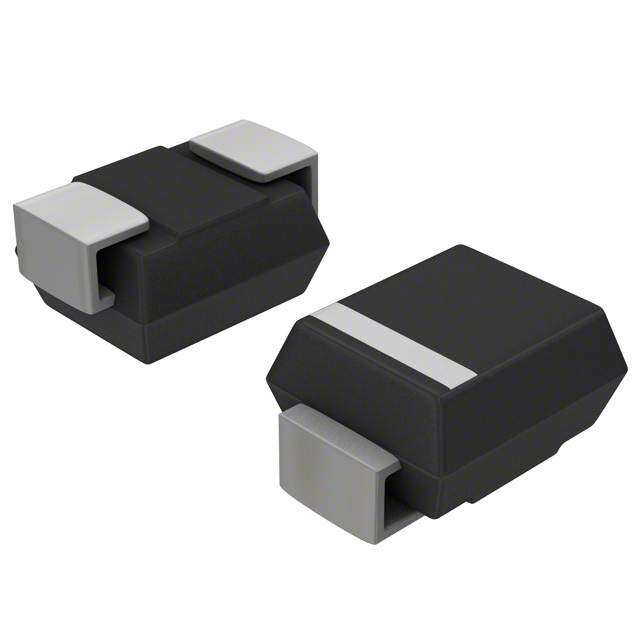
| 描述 | TVS DIODE 5VWM 14VC SOD523TVS 二极管 - 瞬态电压抑制器 BI 10.1 to 20pF 1Ch 2 Pin SOD523 TVS |
| 产品分类 | |
| 品牌 | Diodes Incorporated |
| 产品手册 | |
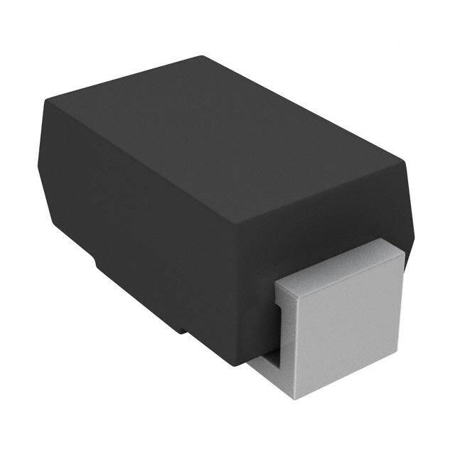
| 产品图片 |
|
| rohs | 符合RoHS无铅 / 符合限制有害物质指令(RoHS)规范要求 |
| 产品系列 | 二极管与整流器,TVS二极管,TVS 二极管 - 瞬态电压抑制器,Diodes Incorporated D5V0L1B2T-7- |
| 数据手册 | |
| 产品型号 | D5V0L1B2T-7 |
| RoHS指令信息 | http://diodes.com/download/4349 |
| 不同频率时的电容 | 15pF @ 1MHz |
| 产品种类 | TVS 二极管 - 瞬态电压抑制器 |
| 供应商器件封装 | SOD-523 |
| 其它名称 | D5V0L1B2T-7DIDKR |
| 击穿电压 | 8 V |
| 功率-峰值脉冲 | 84W |
| 包装 | Digi-Reel® |
| 单向通道 | - |
| 双向通道 | 1 |
| 商标 | Diodes Incorporated |
| 安装类型 | 表面贴装 |
| 安装风格 | SMD/SMT |
| 封装 | Reel |
| 封装/外壳 | SC-79,SOD-523 |
| 封装/箱体 | SOD-523 |
| 尺寸 | 0.9 mm W x 1.3 mm L x 0.65 mm H |
| 峰值浪涌电流 | 6 A |
| 峰值脉冲功率耗散 | 84 W |
| 工作温度 | -65°C ~ 150°C |
| 工作电压 | 5 V |
| 应用 | 通用 |
| 最大工作温度 | + 150 C |
| 最小工作温度 | - 65 C |
| 极性 | Bidirectional |
| 标准包装 | 1 |
| 电压-击穿(最小值) | 6V |
| 电压-反向关态(典型值) | 5V(最小值) |
| 电压-箝位(最大值)@Ipp | 14V |
| 电容 | 20 pF |
| 电流-峰值脉冲(10/1000µs) | 6A (8/20µs) |
| 电源线路保护 | 无 |
| 端接类型 | SMD/SMT |
| 类型 | 齐纳 |
| 系列 | D5V0L1B2 |
| 钳位电压 | 14 V |


- 商务部:美国ITC正式对集成电路等产品启动337调查
- 曝三星4nm工艺存在良率问题 高通将骁龙8 Gen1或转产台积电
- 太阳诱电将投资9.5亿元在常州建新厂生产MLCC 预计2023年完工
- 英特尔发布欧洲新工厂建设计划 深化IDM 2.0 战略
- 台积电先进制程称霸业界 有大客户加持明年业绩稳了
- 达到5530亿美元!SIA预计今年全球半导体销售额将创下新高
- 英特尔拟将自动驾驶子公司Mobileye上市 估值或超500亿美元
- 三星加码芯片和SET,合并消费电子和移动部门,撤换高东真等 CEO
- 三星电子宣布重大人事变动 还合并消费电子和移动部门
- 海关总署:前11个月进口集成电路产品价值2.52万亿元 增长14.8%


PDF Datasheet 数据手册内容提取
D5V0L1B2T-7 LOW CAPACITANCE BIDIRECTIONAL TVS DIODE Features Mechanical Data N Provides ESD Protection per IEC 61000-4-2 Standard: Case: SOD523 O Air ±30kV, Contact ±30kV Case Material: Molded Plastic, “Green” Molding Compound. TI 1 Channel of ESD Protection UL Flammability Classification Rating 94V-0 A Low Channel Input Capacitance Moisture Sensitivity: Level 1 per J-STD-020 M Typically used in Cellular Handsets, Portable Electronics, Terminals: Matte Tin Finish Annealed over Alloy 42 Leadframe R Communication Systems, Computers and Peripherals (Lead-Free Plating). Solderable per MIL-STD-202, Method 208 O Totally Lead-Free & Fully RoHS Compliant (Notes 1 & 2) Weight: 0.001 grams (Approximate) F N Halogen and Antimony Free. “Green” Device (Note 3) I E C SOD523 N A V D 1 2 A Top View Device Schematic Ordering Information (Note 4) D 5V0 L X B X XXX - XX Voltage Capacitance # of Channels Polarity # of Pins Package Packing 5V0: 5.0 Volts X: Extremely Low (<0.5pF) 1: 1 Channel B: Bidirectional 2: 2 Pins LP3: X3-DFN0603-2 7: 7” reel F: Ultra Low (0.5 ~ 1.0pF) 2: 2 Channels (Symmetrical) 3: 3 Pins LP: X1-DFN1006-2 7B: 7” reel (DFN1006 P: Very Low (1.1 ~ 10pF) 4: 4 Channels U: Unidirectional 5: 5 Pins LP4: X2-DFN1006-2 Package Only) L: Low (10.1 ~ 20pF) 6: 6 Channels A: Bidirectional 6: 6 Pins WS: SOD323 13: 13” reel M: Medium (>20pF) (Asymmetrical) 8: 8 Pins T: SOD523/SOT523 10: 10 Pins SO: SOT23/SOT25 W: SOD123/SOT323 TS: TSOT25/TSOT26 S: SOT353/SOT363 V:SOT553/SOT563 Part Number Case Packaging D5V0L1B2T-7 (Note 5) SOD523 3000/Tape & Reel Notes: 1. No purposely added lead. Fully EU Directive 2002/95/EC (RoHS) & 2011/65/EU (RoHS 2) compliant. 2. See http://www.diodes.com/quality/lead_free.html for more information about Diodes Incorporated’s definitions of Halogen- and Antimony-free, "Green" and Lead-free. 3. Halogen- and Antimony-free "Green” products are defined as those which contain <900ppm bromine, <900ppm chlorine (<1500ppm total Br + Cl) and <1000ppm antimony compounds. 4. For packaging details, go to our website at http”//www.diodes.com/products/packages.html 5. Dispensed every other cavity of the carrier tape. Marking Information 6 / 9 6 / 9 = Product Type Marking Code D5V0L1B2T-7 1 of 4 September 2014 Document number: DS35597 Rev. 6 - 2 www.diodes.com © Diodes Incorporated
D5V0L1B2T-7 Maximum Ratings (@TA = +25°C unless otherwise specified.) Characteristic Symbol Value Unit Conditions Peak Pulse Power Dissipation PPP 84 W 8/20µs, per Figure 2 N Peak Pulse Current IPP 6 A 8/20µs, per Figure 2 O ESD Protection – Contact Discharge VESD_Contact ±30 kV IEC 61000-4-2 Standard TI ESD Protection – Air Discharge VESD_Air ±30 kV IEC 61000-4-2 Standard A M Thermal Characteristics R O Characteristic Symbol Value Unit F N Package Power Dissipation (Note 6) PD 275 mW I Thermal Resistance, Junction to Ambient (Note 6) RJA 454 °C/W E Operating and Storage Temperature Range TJ, TSTG -65 to +150 °C C N A Electrical Characteristics V (@TA = +25°C unless otherwise specified.) D Characteristic Symbol Min Typ Max Unit Test Conditions A Reverse Standoff Voltage VRWM - - 5 V - Channel Leakage Current (Note 7) IRM - 10 100 nA VRWM = 5V - 7.0 9.0 IPP = 1A, tp = 8/20μS Clamping Voltage, Positive Transients VCL -- 180.7.5 1120..07 V IIPPPP == 35AA,, ttpp == 88//2200μμSS - 11.5 14.0 IPP = 6A, tp = 8/20μS Breakdown Voltage VBR 6 7 8 V IR = 1mA Differential Resistance RDIF - 0.2 - Ω IR = 1A, tp = 8/20μS Channel Input Capacitance CIN - 15 20 pF VR = 0V, f = 1MHz Notes: 6. Device mounted on FR-4 PCB pad layout (2oz copper) as shown on Diodes, Inc. suggested pad layout AP02001, which can be found on our website at http://www.diodes.com. 7. Short duration pulse test used to minimize self-heating effect. 100 NG % OFURRENT 75 T (%I)pp100 TIC N RAR RE EO 50 R DR U E E C SW E 50 LO S AK PUEAK P 25 K PUL PEP EA P , P P I 0 0 0 25 50 75 100 125 150 175 200 0 20 40 60 TA, AMBIENT TEMPERATURE (°C) t, TIME (s) Fig. 1 Power Dissipation vs. Ambient Temperature Fig. 2 Pulse Waveform D5V0L1B2T-7 2 of 4 September 2014 Document number: DS35597 Rev. 6 - 2 www.diodes.com © Diodes Incorporated
D5V0L1B2T-7 100 18 17 f = 1 MHz ON ENT (nA) 10 TA = 125°C TA = 150°C CE (pF) 16 R N 15 MATI GE CUR TA = 25°CTA = 85°C APACITA 14 R KA TA = -55°C L C 13 O EA 1 TA L O NF I, R , TT12 C I 11 E C 0.1 10 N 0 1 2 3 4 5 6 0 1 2 3 4 5 6 A VR, REVERSE VOLTAGE (V) VR, REVERSE VOLTAGE (V) V Fig. 3 Typical Reverse Characteristics Fig. 4 Typical Total Capacitance vs. Reverse Voltage D 1,000 A W) R ( E W O P E S 100 L U P K A E P , K P P 10 1 10 100 1,000 PULSE WIDTH (µs) Fig. 5 Pulse Rating Curve vs. Pulse Width Power is defined as P = V x I PK C PP Package Outline Dimensions Please see AP02002 at http://www.diodes.com/datasheets/ap02002.pdf for the latest version. L SOD523 Dim Min Max A 0.25 0.35 C H B 0.70 0.90 C 1.50 1.70 H 1.10 1.30 K 0.55 0.65 L 0.10 0.30 M 0.10 0.12 A M All Dimensions in mm B K D5V0L1B2T-7 3 of 4 September 2014 Document number: DS35597 Rev. 6 - 2 www.diodes.com © Diodes Incorporated
D5V0L1B2T-7 Suggested Pad Layout Please see AP02001 at http://www.diodes.com/datasheets/ap02001.pdf for the latest version. N O I T X1 A X Dimensions Value (in mm) M G 0.80 R X 0.60 O X1 2.00 F Y Y 0.70 N I E G C N A V IMPORTANT NOTICE D A DIODES INCORPORATED MAKES NO WARRANTY OF ANY KIND, EXPRESS OR IMPLIED, WITH REGARDS TO THIS DOCUMENT, INCLUDING, BUT NOT LIMITED TO, THE IMPLIED WARRANTIES OF MERCHANTABILITY AND FITNESS FOR A PARTICULAR PURPOSE (AND THEIR EQUIVALENTS UNDER THE LAWS OF ANY JURISDICTION). Diodes Incorporated and its subsidiaries reserve the right to make modifications, enhancements, improvements, corrections or other changes without further notice to this document and any product described herein. Diodes Incorporated does not assume any liability arising out of the application or use of this document or any product described herein; neither does Diodes Incorporated convey any license under its patent or trademark rights, nor the rights of others. Any Customer or user of this document or products described herein in such applications shall assume all risks of such use and will agree to hold Diodes Incorporated and all the companies whose products are represented on Diodes Incorporated website, harmless against all damages. Diodes Incorporated does not warrant or accept any liability whatsoever in respect of any products purchased through unauthorized sales channel. Should Customers purchase or use Diodes Incorporated products for any unintended or unauthorized application, Customers shall indemnify and hold Diodes Incorporated and its representatives harmless against all claims, damages, expenses, and attorney fees arising out of, directly or indirectly, any claim of personal injury or death associated with such unintended or unauthorized application. Products described herein may be covered by one or more United States, international or foreign patents pending. Product names and markings noted herein may also be covered by one or more United States, international or foreign trademarks. This document is written in English but may be translated into multiple languages for reference. Only the English version of this document is the final and determinative format released by Diodes Incorporated. LIFE SUPPORT Diodes Incorporated products are specifically not authorized for use as critical components in life support devices or systems without the express written approval of the Chief Executive Officer of Diodes Incorporated. As used herein: A. Life support devices or systems are devices or systems which: 1. are intended to implant into the body, or 2. support or sustain life and whose failure to perform when properly used in accordance with instructions for use provided in the labeling can be reasonably expected to result in significant injury to the user. B. A critical component is any component in a life support device or system whose failure to perform can be reasonably expected to cause the failure of the life support device or to affect its safety or effectiveness. Customers represent that they have all necessary expertise in the safety and regulatory ramifications of their life support devices or systems, and acknowledge and agree that they are solely responsible for all legal, regulatory and safety-related requirements concerning their products and any use of Diodes Incorporated products in such safety-critical, life support devices or systems, notwithstanding any devices- or systems-related information or support that may be provided by Diodes Incorporated. Further, Customers must fully indemnify Diodes Incorporated and its representatives against any damages arising out of the use of Diodes Incorporated products in such safety-critical, life support devices or systems. Copyright © 2014, Diodes Incorporated www.diodes.com D5V0L1B2T-7 4 of 4 September 2014 Document number: DS35597 Rev. 6 - 2 www.diodes.com © Diodes Incorporated
Mouser Electronics Authorized Distributor Click to View Pricing, Inventory, Delivery & Lifecycle Information: D iodes Incorporated: D5V0L1B2T-7