ICGOO在线商城 > 射频/IF 和 RFID > RF 收发器 IC > CYRF69103-40LTXC

 Datasheet下载
- 型号: CYRF69103-40LTXC
- 制造商: Cypress Semiconductor
- 库位|库存: xxxx|xxxx
- 要求:
| 数量阶梯 | 香港交货 | 国内含税 |
| +xxxx | $xxxx | ¥xxxx |
查看当月历史价格
查看今年历史价格
CYRF69103-40LTXC产品简介:
ICGOO电子元器件商城为您提供CYRF69103-40LTXC由Cypress Semiconductor设计生产,在icgoo商城现货销售,并且可以通过原厂、代理商等渠道进行代购。 CYRF69103-40LTXC价格参考。Cypress SemiconductorCYRF69103-40LTXC封装/规格:RF 收发器 IC, IC 射频 TxRx + MCU 通用 ISM > 1GHZ 2.4GHz 40-VFQFN 裸露焊盘。您可以下载CYRF69103-40LTXC参考资料、Datasheet数据手册功能说明书,资料中有CYRF69103-40LTXC 详细功能的应用电路图电压和使用方法及教程。
| 参数 | 数值 |
| 产品目录 | |
| 描述 | IC PROC 8K FLASH 40QFN射频微控制器 - MCU Programmable Radio on Chip Low Power |
| 产品分类 | RF 收发器集成电路 - IC |
| 品牌 | Cypress Semiconductor |
| 产品手册 | http://www.cypress.com/?docID=42618 |
| 产品图片 |
|
| rohs | 符合RoHS无铅 / 符合限制有害物质指令(RoHS)规范要求 |
| 产品系列 | 嵌入式处理器和控制器,微控制器 - MCU,射频微控制器 - MCU,Cypress Semiconductor CYRF69103-40LTXCPRoC |
| 数据手册 | |
| 产品型号 | CYRF69103-40LTXC |
| 产品种类 | 射频微控制器 - MCU |
| 功率-输出 | 4dBm |
| 包装 | 托盘 |
| 商标 | Cypress Semiconductor |
| 处理器系列 | CYRF69103 |
| 天线连接器 | PCB,表面贴装 |
| 存储容量 | 8kB 闪存,256B SRAM |
| 安装风格 | SMD/SMT |
| 封装 | Tray |
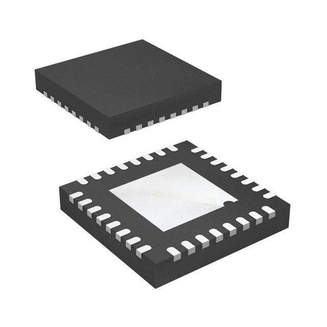
| 封装/外壳 | 40-VFQFN 裸露焊盘 |
| 封装/箱体 | QFN-40 |
| 工作温度 | 0°C ~ 70°C |
| 工作电源电压 | 1.8 V to 3.6 V |
| 工厂包装数量 | 490 |
| 应用 | ISM |
| 数据RAM大小 | 256 B |
| 数据总线宽度 | 8 bit |
| 数据接口 | PCB,表面贴装 |
| 数据速率(最大值) | 1Mbps |
| 最大工作温度 | + 70 C |
| 最大时钟频率 | 2.4 GHz |
| 最小工作温度 | 0 C |
| 标准包装 | 490 |
| 核心 | M8C |
| 灵敏度 | -97dBm |
| 电压-电源 | 1.8 V ~ 3.6 V |
| 电流-传输 | 39.9mA |
| 电流-接收 | 21.9mA |
| 程序存储器大小 | 8 kB |
| 系列 | CYRF69103 |
| 调制或协议 | DSSS,GFSK |
| 频率 | 2.4GHz |


- 商务部:美国ITC正式对集成电路等产品启动337调查
- 曝三星4nm工艺存在良率问题 高通将骁龙8 Gen1或转产台积电
- 太阳诱电将投资9.5亿元在常州建新厂生产MLCC 预计2023年完工
- 英特尔发布欧洲新工厂建设计划 深化IDM 2.0 战略
- 台积电先进制程称霸业界 有大客户加持明年业绩稳了
- 达到5530亿美元!SIA预计今年全球半导体销售额将创下新高
- 英特尔拟将自动驾驶子公司Mobileye上市 估值或超500亿美元
- 三星加码芯片和SET,合并消费电子和移动部门,撤换高东真等 CEO
- 三星电子宣布重大人事变动 还合并消费电子和移动部门
- 海关总署:前11个月进口集成电路产品价值2.52万亿元 增长14.8%


PDF Datasheet 数据手册内容提取
CYRF69103 Programmable Radio-on-Chip Low Power Programmable Radio on Chip Low Power PRoC™ LP Features ❐Each GPIO pin supports high impedance inputs, configurable pull up, open drain output, CMOS/TTL inputs, and CMOS ■Single Device, Two Functions output ❐Maskable interrupts on all I/O pins ❐8-bit Flash based MCU function and 2.4 GHz radio transceiver function in a single device. ■Operating Voltage from 1.8 V to 3.6 V DC ■Flash Based Microcontroller Function ■Operating Temperature from 0 to 70 °C s ❐M8C based 8-bit CPU, optimized for Human Interface n Devices (HID) applications ■Pb-free 40-pin QFN Package g ❐256 Bytes of SRAM ■Advanced Development Tools based on Cypress’s PSoC® i ❐8 Kbytes of Flash memory with EEPROM emulation Tools s ❐In-System reprogrammable e ❐CPU speed up to 12 MHz Applications d ❐16-bit free running timer ❐Low power wakeup timer The CYRF69103 PRoC LP is targeted for the following w applications: ❐12-bit Programmable Interval Timer with interrupts ❐Watchdog timer ■Wireless HID devices: e ■Industry leading 2.4 GHz Radio Transceiver Function ❐Mice n ❐Operates in the unlicensed worldwide Industrial, Scientific, ❐Remote Controls r and Medical (ISM) band (2.4 GHz to 2.483 GHz) ❐Presenter tools o ❐DSSS data rates of up to 250 Kbps ❐Barcode scanners f ❐GFSK data rate of 1 Mbps ❐POS terminal d ❐–97 dBm receive sensitivity ■General purpose wireless applications: ❐Programmable output power up to +4 dBm e ❐Industrial applications ❐Auto Transaction Sequencer (ATS) d ❐Home automation ❐Framing CRC and Auto ACK ❐White goods n ❐Received Signal Strength Indication (RSSI) ❐Consumer electronics e ❐Automatic Gain Control (AGC) ❐Toys m ■Component Reduction Functional Description ❐Integrated 1.8 V boost converter m ❐GPIOs that require no external components PRoC LP devices are integrated radio and microcontroller ❐Operates off a single crystal functions in the same package to provide a dual-role single-chip o ■Flexible I/O solution. c ❐2 mA source current on all GPIO pins. Configurable 8 mA or Communication between the microcontroller and the radio is e 50 mA/pin current sink on designated pins through the radio’s SPI interface. r t o N CypressSemiconductorCorporation • 198 Champion Court • SanJose, CA 95134-1709 • 408-943-2600 Document Number: 001-07611 Rev. *J Revised May 19, 2017
CYRF69103 Logic Block Diagram 47µF VCC MOSI SCK nSS 470nF VCC 10 µF MICRO RST VBat2 VBat1 VBat0 L/D VReg VCC1 VCC2 VCC3 VIO VDD_ s RFbias n RFp g RFn i s Microcontroller Radio e Function Function d IRQ/GPIO P1.5/MOSI w P0_1,3,4,7 MISO/GPIO 4 P1.4/SCK e P1_0:2,6:7 XOUT/GPIO P1.3/nSS 5 n PACTL/GPIO P2_0:1 2 GND Xtal RESV GND. . . . . GND Vdd or f 12 MHz . . . . . . . 470 nF d e d n e m m o c e r t o N Document Number: 001-07611 Rev. *J Page 2 of 72
CYRF69103 Contents Functional Overview ........................................................4 Flash ..........................................................................21 2.4 GHz Radio Function ..............................................4 SROM ........................................................................21 Data Transmission Modes ...........................................4 SROM Function Descriptions ....................................22 Microcontroller Function ..............................................4 Clocking ..........................................................................25 Backward Compatibility ...............................................4 SROM Table Read Description .................................26 DDR Mode ...................................................................5 Clock Architecture Description ..................................27 SDR Mode ..................................................................5 CPU Clock During Sleep Mode .................................31 Pinouts ..............................................................................6 Reset ................................................................................32 Pin Definitions ..................................................................6 Power On Reset ........................................................33 s Functional Block Overview ..............................................7 Watchdog Timer Reset ..............................................33 n 2.4 GHz Radio .............................................................7 Sleep Mode ......................................................................33 g Frequency Synthesizer ................................................7 Sleep Sequence ........................................................33 i Baseband and Framer .................................................7 Low Power in Sleep Mode .........................................34 s Packet Buffers and Radio Configuration Registers .....8 Wakeup Sequence ....................................................34 e Auto Transaction Sequencer (ATS) ............................8 Low Voltage Detect Control ...........................................36 d Interrupts .....................................................................9 POR Compare State .................................................37 Clocks ..........................................................................9 ECO Trim Register ....................................................37 w GPIO Interface ............................................................9 General Purpose I/O Ports .............................................38 Power On Reset/Low Voltage Detect ..........................9 Port Data Registers ...................................................38 e Timers .........................................................................9 GPIO Port Configuration ...........................................39 n Power Management ....................................................9 GPIO Configurations for Low Power Mode ...............44 Low Noise Amplifier (LNA) Serial Peripheral Interface (SPI) ................................45 r o and Received Signal Strength Indication (RSSI) ..............11 SPI Data Register ......................................................46 Receive Spurious Response .....................................11 SPI Configure Register ..............................................46 f SPI Interface ....................................................................11 SPI Interface Pins ......................................................48 d 3-Wire SPI Interface ..................................................11 Timer Registers ..............................................................48 e 4-Wire SPI Interface ..................................................11 Registers ...................................................................48 d SPI Communication and Transactions ......................12 Interrupt Controller .........................................................51 n SPI I/O Voltage References ......................................12 Architectural Description ...........................................51 SPI Connects to External Devices ............................12 Interrupt Processing ..................................................52 e CPU Architecture ............................................................13 Interrupt Latency .......................................................52 m CPU Registers .................................................................14 Interrupt Registers .....................................................52 Flags Register ...........................................................14 Microcontroller Function Register Summary .............56 m Accumulator Register ................................................14 Radio Function Register Summary ...............................58 o Index Register ...........................................................15 Absolute Maximum Ratings ..........................................59 Stack Pointer Register ...............................................15 DC Characteristics .........................................................59 c CPU Program Counter High Register .......................15 AC Characteristics .........................................................61 e CPU Program Counter Low Register ........................15 RF Characteristics ..........................................................65 r Addressing Modes .........................................................16 Ordering Information ......................................................67 t Source Immediate .....................................................16 Ordering Code Definitions .........................................67 o Source Direct .............................................................16 Package Handling ...........................................................68 N Source Indexed .........................................................16 Package Diagrams ..........................................................68 Destination Direct ......................................................16 Acronyms ........................................................................70 Destination Indexed ...................................................17 Document Conventions .................................................70 Destination Direct Source Immediate ........................17 Units of Measure .......................................................70 Destination Indexed Source Immediate ....................17 Document History Page .................................................71 Destination Direct Source Direct ...............................17 Sales, Solutions, and Legal Information ......................72 Source Indirect Post Increment .................................18 Worldwide Sales and Design Support .......................72 Destination Indirect Post Increment ..........................18 Products ....................................................................72 Instruction Set Summary ...............................................19 PSoC® Solutions ......................................................72 Memory Organization .....................................................20 Cypress Developer Community .................................72 Flash Program Memory Organization .......................20 Technical Support .....................................................72 Data Memory Organization .......................................21 Document Number: 001-07611 Rev. *J Page 3 of 72
CYRF69103 Functional Overview Both 64-chip and 32-chip data PN codes are supported. The four data transmission modes apply to the data after the Start of The CYRF69103 is a complete Radio System-on-Chip device, Packet (SOP). In particular, the packet length, data and CRC are providing a complete RF system solution with a single device and all sent in the same mode. a few discrete components. The CYRF69103 is designed to Microcontroller Function implement low cost wireless systems operating in the worldwide 2.4 GHz Industrial, Scientific, and Medical (ISM) frequency band The MCU function is an 8-bit Flash-programmable (2.400GHz to 2.4835 GHz). microcontroller. The instruction set is optimized specifically for HID and a variety of other embedded applications. 2.4 GHz Radio Function The MCU function has up to 8 Kbytes of Flash for user’s code The SoC contains a 2.4 GHz 1 Mbps GFSK radio transceiver, and up to 256 bytes of RAM for stack space and user variables. s packet data buffering, packet framer, DSSS baseband controller, Received Signal Strength Indication (RSSI), and SPI interface In addition, the MCU function includes a Watchdog timer, a n for data transfer and device configuration. vectored interrupt controller, a 16-bit Free Running Timer, and g 12-bit Programmable Interrupt Timer. The radio supports 98 discrete 1 MHz channels (regulations may i limit the use of some of these channels in certain jurisdictions). The microcontroller has 15 GPIO pins grouped into multiple s In DSSS modes the baseband performs DSSS ports. With the exception of the four radio function GPIOs, each e spreading/despreading, while in GFSK Mode (1 Mb/s - GFSK) GPIO port supports high impedance inputs, configurable pull up, d the baseband performs Start of Frame (SOF), End of Frame open drain output, CMOS/TTL inputs and CMOS output. Up to (EOF) detection, and CRC16 generation and checking. The two pins support programmable drive strength of up to 50 mA. w baseband may also be configured to automatically transmit Additionally, each I/O pin can be used to generate a GPIO Acknowledge (ACK) handshake packets whenever a valid interrupt to the microcontroller. Each GPIO port has its own GPIO e packet is received. interrupt vector with the exception of GPIO Port 0. GPIO Port 0 n has two dedicated pins that have independent interrupt vectors When in receive mode, with packet framing enabled, the device (P0.3–P0.4). is always ready to receive data transmitted at any of the r supported bit rates, except SDR, enabling the implementation of The microcontroller features an internal oscillator. o mixed-rate systems in which different devices use different data The PRoC LP includes a Watchdog timer, a vectored interrupt f rates. This also enables the implementation of dynamic data rate controller, a 12-bit programmable interval timer with configurable d systems, which use high data rates at shorter distances and/or 1 ms interrupt and a 16-bit free running timer. e in a low moderate interference environment, and change to lower In addition, the CYRF69103 IC has a Power Management Unit data rates at longer distances and/or in high interference d (PMU), which enables direct connection of the device to any environments. battery voltage in the range 1.8 V to 3.6 V. The PMU conditions n The radio meets the following worldwide regulatory the battery voltage to provide the supply voltages required by the e requirements: device and may supply external devices. m ■Europe: Backward Compatibility ❐ETSI EN 301 489-1 V1.4.1 m The CYRF69103 IC is fully interoperable with the main modes of ❐ETSI EN 300 328-1 V1.3.1 the first generation Cypress radios namely the CYWUSB6934 o ■North America: -LS and CYWWUSB6935-LR devices. The 62.5 kbps mode is c ❐FCC CFR 47 Part 15 supported by selecting 32 chip DDR mode. Similarly, the e 15.675kbps mode is supported by selecting 64 chip SDR mode ■Japan: r In this method, a suitably configured CYRF69103 IC device may ❐ARIB STD-T66 transmit data to or receive data from a first generation device, or t Data Transmission Modes both. Backwards compatibility requires disabling the SOP, o length, and CRC16 fields. N The radio supports four different data transmission modes: This section provides the different configurations of the registers ■In GFSK mode, data is transmitted at 1 Mbps, without any and firmware that enable a new generation radio to communicate DSSS with a first generation radio. There are two possible modes: SDR and DDR mode (8-DR and GFSK modes are not present in the ■In 8DR mode, 1 byte is encoded in each PN code symbol first generation radio). The second generation radio must be transmitted initialized using the RadioInitAPI of the LP radio driver and then ■In DDR mode, 2 bits are encoded in each PN code symbol the following registers’ bits need to be configured to the given transmitted Byte values. Essentially, the following deactivates the added features of the second generation radio and takes it down to the ■In SDR mode, a single bit is encoded in each PN code symbol level of the first generation radio. The data format, data rates, transmitted and the PN codes used are recognizable by the first generation radio. Document Number: 001-07611 Rev. *J Page 4 of 72
CYRF69103 DDR Mode Table 1. DDR Mode Register Value Description TX_CFG_ADR 0X16 32 chip PN Code, DDR, PA = 6 RX_CFG_ADR 0X4B AGC is enabled. LNA and attenuator are disabled. Fast turnaround is disabled, the device uses high side receive injection and Hi-Lo is disabled. Overwrite to receive buffer is enabled and the RX buffer is configured to receive eight bytes maximum. XACT_CFG_ADR 0X05 AutoACK is disabled. Forcing end state is disabled. The device is configured to transition to Idle mode after a Receive or Transmit. ACK timeout is set to 128 µs. s FRAMING_CFG_ADR 0X00 All SOP and framing features are disabled. Disable LEN_EN = 0 if EOP is needed. n TX_OVERRIDE_ADR 0X04 Disable Transmit CRC-16. g RX_OVERRIDE_ADR 0X14 The receiver rejects packets with a zero seed. The Rx CRC-16 Checker is disabled and i the receiver accepts bad packets that do not match the seed in CRC_seed registers. This s helps in communication with the first generation radio that does not have CRC capabilities. e ANALOG_CTRL_ADR 0X01 Set ALL SLOW. When set, the synthesizer settle time for all channels is the same as the d slow channels in the first generation radio. w DATA32_THOLD_ADR 0X03 Sets the number of allowed corrupted bits to 3. EOP_CTRL_ADR 0x01 Sets the number of consecutive symbols for non-correlation to detect end of packet. e PREAMBLE_ADR 0xAAAA05 AAAA are the two preamble bytes. Any other byte can also be written into the preamble n register file. Recommended counts of the preamble bytes to be sent must be >4. r o SDR Mode f Table 2. SDR Mode d Register Value Description e TX_CFG_ADR 0X3E 64 chip PN code, SDR mode, PA = 6 d RX_CFG_ADR 0X4B AGC is enabled. LNA and attenuator are disabled. Fast turnaround is disabled, the device n uses high side receive injection and Hi-Lo is disabled. Overwrite to receive buffer is e enabled and RX buffer is configured to receive eight bytes maximum. Enables RXOW to allow new packets to be loaded into the receive buffer. This also enables the VALID bit m which is used by the first generation radio’s error correction firmware. m XACT_CFG_ADR 0X05 AutoACK is disabled. Forcing end state is disabled. The device is configured to transition to Idle mode after Receive or Transmit. ACK timeout is set to 128 µs. o FRAMING_CFG_ADR 0X00 All SOP and framing features are disabled. Disable LEN_EN=0 if EOP is needed. c TX_OVERRIDE_ADR 0X04 Disable Transmit CRC-16. e RX_OVERRIDE_ADR 0X14 The receiver rejects packets with a zero seed. The RX CRC-16 checker is disabled and r the receiver accepts bad packets that do not match the seed in the CRC_seed registers. t This helps in communication with the first generation radio that does not have CRC o capabilities. N ANALOG_CTRL_ADR 0X01 Set ALL SLOW. When set, the synthesizer settle time for all channels is the same as the slow channels in the first generation radio, for manual ACK consistency DATA64_THOLD_ADR 0X07 Sets the number of allowed corrupted bits to 7 which is close to the recommended 12% value. EOP_CTRL_ADR 0xA1 Sets the number of consecutive symbols for non-correlation to detect end of packet. PREAMBLE_ADR 0xAAAA09 AAAA are the two preamble bytes. Any other byte can also be written into the preamble register file. Recommended counts of the preamble bytes to be sent must be >8. Document Number: 001-07611 Rev. *J Page 5 of 72
CYRF69103 Pinouts Figure 1. Pin Diagram P A C T L Ctoarbnser REGV BAT0V P0.7 L/D DD_1.8V P1.7 RST IOV P1.6 / GPIO 4 3 3 3 3 3 3 3 3 3 0 9 8 7 6 5 4 3 2 1 P0.4 1 30 XOUT / GPIO s XTAL 2 29 MISO / GPIO n CYRF69103 VCC 3 PRoC LP 28 P1.5 / MOSI g P0.3 4 27 IRQ / GPIO i s P0.1 5 26 P1.4 / SCK e VBAT1 6 25 P1.3 / SS d VCC 7 24 P1.2 P2.1 8 23 VDD_Micro w VBAT2 9 * E-PAD Bottom Side 22 P1.1 e RFBIAS 10 21 P1.0 n 1 1 1 1 1 1 1 1 1 2 1 2 3 4 5 6 7 8 9 0 r PRF GND NRF NC P2.0 CCV NC NC RES NC o V f d Pin Definitions e d Pin Name Description n 1 P0.4 Individually configured GPIO e 2 XTAL 12 MHz crystal m 3, 7, 16 V 2.4 V to 3.6 V supply. Connected to pin 40 (0.047 F bypass) CC 4 P0.3 Individually configured GPIO m 5 P0.1 Individually configured GPIO o 6 V Connect to 1.8 V to 3.6 V power supply, through 47 ohm series/1 F shunt C. bat1 c 8 P2.1 GPIO. Port 2 Bit 1 e 9 Vbat2 Connected to1.8 V to 3.6 V main power supply, through 0.047 F bypass C. r 10 RFbias RF pin voltage reference t o 11 RF Differential RF to or from antenna p N 12 GND GND 13 RF Differential RF to or from antenna n 14, 17, 18, 20 NC 15 P2.0 GPIO 19 RESV Reserved. Must connect to GND 21 P1.0 GPIO port 1 bit 0 / ISSP-SCLK If this pin is used as a general-purpose output it draws current. It is, therefore, configured as an input to reduce current draw. 22 P1.1 GPIO port 1 bit 1 / ISSP-SDATA If this pin is used as a general-purpose output it draws current. It is, therefore, configured as an input to reduce current draw. 23 V MCU supply connected to pin 40, max CPU 12 MHz DD_micro Document Number: 001-07611 Rev. *J Page 6 of 72
CYRF69103 Pin Definitions (continued) Pin Name Description 24 P1.2 GPIO 25 P1.3 / nSS Slave Select 26 P1.4 / SCK SPI Clock 27 IRQ Radio Function Interrupt output, configure High, Low or as Radio GPIO. 28 P1.5 / MOSI MOSI pin from microcontroller function to radio function. 29 MISO 3-wire SPI mode configured as Radio GPIO. In 4-wire SPI mode sends data to MCU function. s 30 XOUT Buffered CLK, PACTL_n or Radio GPIO. n 31 PACTL Control for external PA or Radio GPIO. g 32 P1.6 GPIO i s 33 V 1.8 V to 3.6V to main power supply rail for Radio I/O. IO e 34 RST Radio Reset. Connected to pin 40 with 0.47 F. Must have a RST = HIGH event the very first time d power is applied to the radio otherwise the state of the radio control registers is unknown. 35 P1.7 GPIO w 36 V Regulated logic bypass. Connected to 0.47 F to GND. DD1.8 e 37 L/D Inductor/Diode connection for Boost. When Internal PMU is not being used connect L/D to GND. n 38 P0.7 GPIO r 39 V Connected to1.8 V to 3.6 V main power supply, through 0.047 F bypass C. bat0 o 40 V Boost regulator output voltage feedback REG f 41 E-pad Must be connected to ground. d 42 Corner Tabs Do Not connect corner tabs. e d Functional Block Overview Frequency Synthesizer n Before transmission or reception may commence, it is necessary All the blocks that make up the PRoC LP are presented in this e for the frequency synthesizer to settle. The settling time varies section. depending on channel; 25 fast channels are provided with a m maximum settling time of 100 s. 2.4 GHz Radio m The “fast channels” (<100 s settling time) are every 3rd The radio transceiver is a dual conversion low IF architecture frequency, starting at 2400 MHz up to and including 2472 MHz optimized for power and range/robustness. The radio employs o (that is, 0,3,6,9…….69 and 72). channel matched filters to achieve high performance in the c presence of interference. An integrated Power Amplifier (PA) Baseband and Framer e provides up to +4 dBm transmit power, with an output power control range of 34 dB in eight steps. The supply current of the The baseband and framer blocks provide the DSSS encoding r device is reduced as the RF output power is reduced. and decoding, SOP generation and reception and CRC16 t generation and checking, and EOP detection and length field. o Table 3. Internal PA Output Power Step Table N Data Transmission Modes and Data Rates PA Setting Typical Output Power (dBm) The SoC supports four different data transmission modes: 7 +4 ■In GFSK mode, data is transmitted at 1 Mbps, without any 6 0 DSSS. 5 –5 ■In 8DR mode, 8 bits are encoded in each DATA_CODE_ADR 4 –10 derived code symbol transmitted. 3 –15 ■In DDR mode, 2 bits are encoded in each DATA_CODE_ADR 2 –20 derived code symbol transmitted (as in the CYWUSB6934 DDR mode). 1 –25 0 –30 ■In SDR mode, 1 bit is encoded in each DATA_CODE_ADR derived code symbol transmitted (as in the CYWUSB6934 standard modes). Document Number: 001-07611 Rev. *J Page 7 of 72
CYRF69103 Both 64-chip and 32-chip DATA_CODE_ADR codes are EOP – There are two options for detecting the end of a packet. supported. The four data transmission modes apply to the data If SOP is enabled, then a packet length field may be enabled. after the SOP. In particular the length, data, and CRC16 are all GFSK and 8DR must enable the length field. This is the first sent in the same mode. In general, lower data rates reduces 8bits after the SOP symbol, and is transmitted at the payload packet error rate in any given environment. data rate. If the length field is enabled, an End of Packet (EOP) condition is inferred after reception of the number of bytes The CYRF69103 IC supports the following data rates: defined in the length field, plus two bytes for the CRC16 (if ■1000 kbps (GFSK) enabled). The alternative to using the length field is to infer an EOP condition from a configurable number of successive non ■250 kbps (32-chip 8DR) correlations; this option is not available in GFSK mode and is ■125 kbps (64-chip 8DR) only recommended when using SDR mode. s CRC16 – The device may be configured to append a 16-bit ■62.5 kbps (32-chip DDR) CRC16 to each packet. The CRC16 uses the USB CRC n ■31.25 kbps (64-chip DDR) polynomial with the added programmability of the seed. If g enabled, the receiver verifies the calculated CRC16 for the ■15.625 kbps (64-chip SDR) i payload data against the received value in the CRC16 field. The s Lower data rates typically provide longer range and/or a more starting value for the CRC16 calculation is configurable, and the e robust link. CRC16 transmitted may be calculated using either the loaded d seed value or a zero seed; the received data CRC16 is checked Link Layer Modes against both the configured and zero CRC16 seeds. w The CYRF69103 IC device supports the following data packet CRC16 detects the following errors: framing features: e ■ Any one bit in error SOP – Packets begin with a 2-symbol Start of Packet (SOP) n marker. This is required in GFSK and 8DR modes, but is optional ■Any two bits in error (no matter how far apart, which column, in DDR mode and is not supported in SDR mode. If framing is and so on) r disabled then an SOP event is inferred whenever two successive o ■Any odd number of bits in error (no matter where they are) correlations are detected. The SOP_CODE_ADR code used for f the SOP is different from that used for the “body” of the packet, ■An error burst as wide as the checksum itself d and if desired may be a different length. SOP must be configured to be the same length on both sides of the link. Figure2 shows an example packet with SOP, CRC16 and e lengths fields enabled. d n Figure 2. Example Default Packet Format e Preamble 2nd Framing m n x 16us Symbol* m P SOP 1 SOP 2 Length Payload Data CRC 16 o Packet c 1st Framing length Symbol* e 1 Byte *Note:32 or 64us Period r t Packet Buffers and Radio Configuration Registers The CYRF69103 IC supports packet length of up to 40 bytes; o interrupts are provided to allow an MCU to use the transmit and Packet data and configuration registers are accessed through N receive buffers as FIFOs. When transmitting a packet longer the SPI interface. All configuration registers are directly than 16 bytes, the MCU can load 16 bytes initially, and add addressed through the address field in the SPI packet (as in the further bytes to the transmit buffer as transmission of data CYWUSB6934). Configuration registers are provided to allow creates space in the buffer. Similarly, when receiving packets configuration of DSSS PN codes, data rate, operating mode, longer than 16 bytes, the MCU must fetch received data from the interrupt masks, interrupt status, and others. FIFO periodically during packet reception to prevent it from overflowing. Packet Buffers All data transmission and reception use the 16-byte packet Auto Transaction Sequencer (ATS) buffers: one for transmission and one for reception. The CYRF69103 IC provides automated support for The transmit buffer allows a complete packet of up to 16 bytes of transmission and reception of acknowledged data packets. payload data to be loaded in one burst SPI transaction, and then When transmitting a data packet, the device automatically starts transmitted with no further MCU intervention. Similarly, the the crystal and synthesizer, enters transmit mode, transmits the receive buffer allows an entire packet of payload data up to 16 packet in the transmit buffer, and then automatically switches to bytes to be received with no firmware intervention required until receive mode and waits for a handshake packet – and then packet reception is complete. Document Number: 001-07611 Rev. *J Page 8 of 72
CYRF69103 automatically reverts to sleep mode or idle mode when either an The MCU function features an internal oscillator. The clock ACK packet is received, or a time out period expires. generator provides the 12 MHz and 24 MHz clocks that remain internal to the microcontroller. Similarly, when receiving in transaction mode, the device waits in receive mode for a valid packet to be received, then GPIO Interface automatically transitions to transmit mode, transmits an ACK packet, and then switches back to receive mode to await the next The MCU function features up to 15 general purpose I/O (GPIO) packet. The contents of the packet buffers are not affected by the pins.The I/O pins are grouped into three ports (Port 0 to 2). The transmission or reception of ACK packets. pins on Port 0 and Port 1 may each be configured individually while the pins on Port 2 may only be configured as a group. Each In each case, the entire packet transaction takes place without GPIO port supports high-impedance inputs, configurable pull up, any need for MCU firmware action; to transmit data the MCU open drain output, CMOS/TTL inputs, and CMOS output with up simply needs to load the data packet to be transmitted, set the s to two pins that support programmable drive strength of up to length, and set the TX GO bit. Similarly, when receiving packets 50mA sink current. Additionally, each I/O pin can be used to n in transaction mode, firmware simply needs to retrieve the fully generate a GPIO interrupt to the microcontroller. Each GPIO port g received packet in response to an interrupt request indicating has its own GPIO interrupt vector with the exception of GPIO reception of a packet. i Port 0. GPIO Port 0 has three dedicated pins that have s Interrupts independent interrupt vectors (P0.1, P0.3–P0.4). e The radio function provides an interrupt (IRQ) output, which is Power On Reset/Low Voltage Detect d configurable to indicate the occurrence of various different events. The IRQ pin may be programmed to be either active high The power on reset circuit detects logic when power is applied w to the device, resets the logic to a known state, and begins or active low, and be either a CMOS or open drain output. executing instructions at Flash address 0x0000. When power e The radio function features three sets of interrupts: transmit, falls below a programmable trip voltage, it generates reset or n receive, and system interrupts. These interrupts all share a may be configured to generate interrupt. There is a low voltage single pin (IRQ), but can be independently enabled/disabled. In detect circuit that detects when V drops below a CC r transmit mode, all receive interrupts are automatically disabled, programmable trip voltage. It may be configurable to generate an o and in receive mode all transmit interrupts are automatically LVD interrupt to inform the processor about the low voltage f disabled. However, the contents of the enable registers are event. POR and LVD share the same interrupt. There is not a preserved when switching between transmit and receive modes. separate interrupt for each. The Watchdog timer can be used to d If more than one radio interrupt is enabled at any time, it is ensure the firmware never gets stalled in an infinite loop. e necessary to read the relevant status register to determine which Timers d event caused the IRQ pin to assert. Even when a given interrupt n source is disabled, the status of the condition that would The free running 16-bit timer provides two interrupt sources: the otherwise cause an interrupt can be determined by reading the programmable interval timer with 1-s resolution and the e appropriate status register. It is therefore possible to use the 1.024ms outputs. The timer can be used to measure the m devices without making use of the IRQ pin by polling the status duration of an event under firmware control by reading the timer register(s) to wait for an event, rather than using the IRQ pin. at the start and at the end of an event, then calculating the m difference between the two values. Clocks o Power Management A 12 MHz crystal (30 ppm or better) is directly connected c between XTAL and GND without the need for external The operating voltage of the device is 1.8V to 3.6V DC, which is e capacitors. A digital clock out function is provided, with applied to the V pin. The device can be shut down to a fully BAT selectable output frequencies of 0.75, 1.5, 3, 6, or 12 MHz. This static sleep mode by writing to the FRC END = 1 and r output may be used to clock an external microcontroller (MCU) ENDSTATE= 000 bits in the XACT_CFG_ADR register over the t or ASIC. This output is enabled by default, but may be disabled. SPI interface. The device enters sleep mode within 35 s after o The requirements for the crystal to be directly connected to XTAL the last SCK positive edge at the end of this SPI transaction. N Alternatively, the device may be configured to automatically pin and GND are: enter sleep mode after completing packet transmission or ■Nominal Frequency: 12 MHz reception. When in sleep mode, the on-chip oscillator is stopped, but the SPI interface remains functional. The device wakes from ■Operating Mode: Fundamental Mode sleep mode automatically when the device is commanded to ■Resonance Mode: Parallel Resonant enter transmit or receive mode. When resuming from sleep mode, there is a short delay while the oscillator restarts. The ■Frequency Initial Stability: ±30 ppm device may be configured to assert the IRQ pin when the oscillator has stabilized. ■Series Resistance: <60 ohms The output voltage (V ) of the Power Management Unit ■Load Capacitance: 10 pF REG (PMU) is configurable to several minimum values between 2.4 V ■Drive Level: l00 W and 2.7 V. VREG may be used to provide up to 15 mA (average load) to external devices. It is possible to disable the PMU, and to provide an externally regulated DC supply voltage to the device in the range 2.4 V to 3.6 V. The PMU also provides a regulated 1.8 V supply to the logic. Document Number: 001-07611 Rev. *J Page 9 of 72
CYRF69103 The PMU has been designed to provide high boost efficiency Figure 3. PMU Enabled (74–85% depending on input voltage, output voltage and load) when using a Schottky diode and power inductor, eliminating the VBat VCC need for an external boost converter in many systems where 1 Ohm 1% other components require a boosted voltage. However, 10 µF reasonable efficiencies (69–82% depending on input voltage, 6.3V 0.047 µF output voltage and load) may be achieved when using low-cost 47 Ohm 0.047 µF components such as SOT23 diodes and 0805 inductors. 1 µF 6.3V The current through the diode must stay within the linear 0.047 µF operating range of the diode. For some loads the SOT23 diode is sufficient, but with higher loads it is not and a SS12 diode must 0.047µF 0.047 µF s be used to stay within this linear range of operation. Along with the diode, the inductor used must not saturate its core. In higher 0.047 µF n loads, a lower resistance/higher saturation coil like the inductor g from Sumida must be used. VBat2 VBat1 VBat0 VIO VReg VCC1 VCC2 VCC3 si The PMU also provides a configurable low battery detection function which may be read over the SPI interface. One of seven e thresholds between 1.8 V and 2.7 V may be selected. The VDD d interrupt pin may be configured to assert when the voltage on the VBAT pin falls below the configured threshold. LV IRQ is not a VDD_MICRO PRoC LP w latched event. Battery monitoring is disabled when the device is in sleep mode. e 0.1µF The following three figures show different examples of how to n umsoes tP cRoomCm LoPn cwiritchu iat nmda wkiinthgo uust eth oef PthMeU P. MFUig utore b3o osshto bwast tethrey L/D r o voltage up to 2.7 V. Figure4 is an example of the circuit used VBat VCC when the supply voltage is always above 2.7 V. This could be f three 1.5 V battery cells in series along with a linear regulator, or 100 µF 10V 10 µH BAT400D 10 µF 6.3V d some similar power source. Figure5 shows an example of using e the PRoC LP with its PMU disabled and an external boost to supply power to the device. This might be required when the load d is much greater than the 15 mA average load that PRoC can Figure 4. PMU Disabled - Linear Regulator n support. e VCC m m 0.047µF 0.047µF o 0.047µF 0.047µF c 0.047µF e r 0.047µF 0.047µF t 0.047µF o N VBat2 VBat1 VBat0 VIO VReg VCC1 VCC2 VCC3 VDD VDD_MICRO PRoC LP 0.1µF D L/ Document Number: 001-07611 Rev. *J Page 10 of 72
CYRF69103 Figure 5. PMU Disabled - External Boost Converter operating at the transmit spur frequency may receive the spur if the spur level power is greater than the receive sensitivity level. VCC External DC-DC VBat The workaround for this is to program an additional byte in the Boost Converter packet header which contains the transmitter channel number. After the packet is received, the channel number can be 1 Ohm 1% checked. If the channel number does not match the receive 10µF channel then the packet is rejected. 0.047µF 6.3V 47 Ohm SPI Interface 0.047µF 1µF 6.3V 0.047µF The SPI interface between the MCU function and the radio s function is a 3-wire SPI Interface. The three pins are MOSI 0.047µF 0.047µF (Master Out Slave In), SCK (Serial Clock), SS (Slave Select). n There is an alternate 4-wire MISO Interface that requires the g 0.047µF connection of two external pins. The SPI interface is controlled i by configuring the SPI Configure Register. (SPICR Addr: 0x3D). s VBat2 VBat1 VBat0 VIO VReg VCC1 VCC2 VCC3 3-Wire SPI Interface e d The radio function receives a clock from the MCU function on the VDD SBCidKire cptiino.n aTlh dea taM tOraSnIs fpeirn t aikse sm pulaltcipele bxeetdw ewenith th eth Me CMUI SfuOn cptioinn. w VDD_MICRO PRoC LP and the radio function through this multiplexed MOSI pin. When e using this mode the user firmware must ensure that the MOSI pin n on the MCU function is in a high impedance state, except when 0.1µF the MCU is actively transmitting data. Firmware must also control r the direction of data flow and switch directions between MCU o D L/ function and radio function by setting the SWAP bit [Bit 7] of the f SPI Configure Register. The SS pin is asserted before initiating a data transfer between the MCU function and the radio function. d The IRQ function may be optionally multiplexed with the MOSI e Low Noise Amplifier (LNA) and Received Signal pin; when this option is enabled the IRQ function is not available d while the SS pin is low. When using this configuration, user Strength Indication (RSSI) firmware must ensure that the MOSI function on MCU function n The gain of the receiver may be controlled directly by clearing is in a high-impedance state whenever SS is high. e the AGC EN bit and writing to the Low Noise Amplifier (LNA) bit of the RX_CFG_ADR register. When the LNA bit is cleared, the Figure 6. 3-Wire SPI Mode m receiver gain is reduced by approximately 20 dB, allowing m awchceunr aotep ereracteinpgti oan oref cveeivrye rs tvroenryg rcelocseeiv etod sthigen atrlas n(sfomr iettxear)m. pAlne MOSI SCK nSS o additional 20 dB of receiver attenuation can be added by setting the Attenuation (ATT) bit; this allows data reception to be limited c to devices at very short ranges. Disabling AGC and enabling e LNA is recommended unless receiving from a device using external PA. MCU Function Radio Function r t The RSSI register returns the relative signal strength of the o on-channel signal power. P1.5/MOSI MOSI N MOSI/MISO multiplexed When receiving, the device may be configured to automatically on one MOSI pin measure and store the relative strength of the signal being received as a 5-bit value. When enabled, an RSSI reading is P1.4/SCK SCK taken and may be read through the SPI interface. An RSSI reading is taken automatically when the start of a packet is detected. In addition, a new RSSI reading is taken every time the P1.3/nSS nSS previous reading is read from the RSSI register, allowing the background RF energy level on any given channel to be easily measured when RSSI is read when no signal is being received. A new reading can occur as fast as once every 12 s. 4-Wire SPI Interface Receive Spurious Response The 4-wire SPI communications interface consists of MOSI, The transmitter may exhibit spurs around 50MHz offset at levels MISO, SCK, and SS. approximately 50dB to 60dB below the carrier power. Receivers Document Number: 001-07611 Rev. *J Page 11 of 72
CYRF69103 The device receives SCK from the MCU function on the SCK pin. byte. The following bytes are data bytes. The SPI transaction Data from the MCU function is shifted in on the MOSI pin. Data format is shown in Figure4. to the MCU function is shifted out on the MISO pin. The active The DIR bit specifies the direction of data transfer. 0 = Master low SS pin must be asserted for the two functions to reads from slave. 1 = Master writes to slave. communicate. The IRQ function may be optionally multiplexed with the MOSI pin; when this option is enabled the IRQ function The INC bit helps to read or write consecutive bytes from is not available while the SS pin is low. When using this contiguous memory locations in a single burst mode operation. configuration, user firmware must ensure that the MOSI function If Slave Select is asserted and INC = 1, then the master MCU on MCU function is in a high-impedance state whenever SS is function reads a byte from the radio, the address is incremented high. by a byte location, and then the byte at that location is read, and so on. Figure 7. 4-Wire SPI Mode s If Slave Select is asserted and INC = 0, then the MCU function n MOSI SCK nSS rite ias das r/ewgriitsetes rt fhilee bthyetens i ti nre tahdes /swarmitees r tehgeis bteytre isn ibnu thrsatt mreogdiset,e br ufitle if. g The SPI interface between the radio function and the MCU is not i s dependent on the internal 12 MHz oscillator of the radio. e Therefore, radio function registers can be read from or written MCU Function Radio Function into while the radio is in sleep mode. d SPI I/O Voltage References w P1.5/MOSI MOSI The SPI interfaces between MCU function and the radio and the e P1.6/MISO MISO IRQ and RST have a separate voltage reference VIO. For P1.4/SCK SCK n CYRF69103 V is normally set to V . IO CC SPI Connects to External Devices r P1.3/nSS nSS o The three SPI wires, MOSI, SCK, and SS are also drawn out of f the package as external pins to allow the user to interface their own external devices (such as optical sensors and others) d through SPI. The radio function also has its own SPI wires MISO e This connection is external to the PRoC LP Chip and IRQ, which can be used to send data back to the MCU d function or send an interrupt request to the MCU function. They can also be configured as GPIO pins. n SPI Communication and Transactions e The SPI transactions can be single byte or multi-byte. The MCU m function initiates a data transfer through a Command/Address m Table 4. SPI Transaction Format o Byte 1 Byte 1+N c Bit # 7 6 [5:0] [7:0] e Bit Name DIR INC Address Data r t o N Document Number: 001-07611 Rev. *J Page 12 of 72
CYRF69103 CPU Architecture The Accumulator Register (CPU_A) is the general-purpose register that holds the results of instructions that specify any of This family of microcontrollers is based on a high-performance, the source addressing modes. 8-bit, Harvard architecture microprocessor. Five registers control The Index Register (CPU_X) holds an offset value that is used the primary operation of the CPU core. These registers are in the indexed addressing modes. Typically, this is used to affected by various instructions, but are not directly accessible address a block of data within the data memory space. through the register space by the user. The Stack Pointer Register (CPU_SP) holds the address of the current top-of-stack in the data memory space. It is affected by Table 5. CPU Registers and Register Name the PUSH, POP, LCALL, CALL, RETI, and RET instructions, Register Register Name which manage the software stack. It can also be affected by the Flags CPU_F SWAP and ADD instructions. s The Flag Register (CPU_F) has three status bits: Zero Flag bit n Program Counter CPU_PC [1]; Carry Flag bit [2]; Supervisory State bit [3]. The Global g Accumulator CPU_A Interrupt Enable bit [0] is used to globally enable or disable i Stack Pointer CPU_SP interrupts. The user cannot manipulate the Supervisory State s status bit [3]. The flags are affected by arithmetic, logic, and shift Index CPU_X e operations. The manner in which each flag is changed is dependent upon the instruction being executed (for example, d The 16-bit Program Counter Register (CPU_PC) allows for direct AND, OR, XOR). See Table 22 on page 19. addressing of the full eight Kbytes of program memory space. w e n r o f d e d n e m m o c e r t o N Document Number: 001-07611 Rev. *J Page 13 of 72
CYRF69103 CPU Registers Flags Register The Flags Register can only be set or reset with logical instruction. Table 6. CPU Flags Register (CPU_F) [R/W] Bit # 7 6 5 4 3 2 1 0 Field Reserved XIO Super Carry Zero Global IE Read/Write – – – R/W R RW RW RW s Default 0 0 0 0 0 0 1 0 n Bits 7:5 Reserved g Bit 4 XIO Set by the user to select between the register banks. si 0 = Bank 0 e 1 = Bank 1 d Bit 3 Super Indicates whether the CPU is executing user code or Supervisor Code (This code cannot be accessed directly w by the user). 0 = User Code e 1 = Supervisor Code n Bit 2 Carry r Set by CPU to indicate whether there has been a carry in the previous logical/arithmetic operation. o 0 = No Carry f 1 = Carry d Bit 1 Zero Set by CPU to indicate whether there has been a zero result in the previous logical/arithmetic operation. e 0 = Not Equal to Zero d 1 = Equal to Zero n Bit 0 Global IE e Determines whether all interrupts are enabled or disabled. m 0 = Disabled 1 = Enabled m Note This register is readable with explicit address 0xF7. The OR F, expr and AND F, expr must be used to set and clear the CPU_F bits. o c Accumulator Register e r Table 7. CPU Accumulator Register (CPU_A) t Bit # 7 6 5 4 3 2 1 0 o N Field CPU Accumulator [7:0] Read/Write – – – – – – – – Default 0 0 0 0 0 0 0 0 Bits 7:0 CPU Accumulator [7:0] 8-bit data value holds the result of any logical/arithmetic instruction that uses a source addressing mode. Document Number: 001-07611 Rev. *J Page 14 of 72
CYRF69103 Index Register Table 8. CPU X Register (CPU_X) Bit # 7 6 5 4 3 2 1 0 Field X [7:0] Read/Write – – – – – – – – Default 0 0 0 0 0 0 0 0 Bits 7:0 X [7:0] 8-bit data value holds an index for any instruction that uses an indexed addressing mode. s n Stack Pointer Register g Table 9. CPU Stack Pointer Register (CPU_SP) i s Bit # 7 6 5 4 3 2 1 0 e Field Stack Pointer [7:0] d Read/Write – – – – – – – – w Default 0 0 0 0 0 0 0 0 e Bits 7:0 Stack Pointer [7:0] n 8-bit data value holds a pointer to the current top-of-stack. r o CPU Program Counter High Register f Table 10. CPU Program Counter High Register (CPU_PCH) d e Bit # 7 6 5 4 3 2 1 0 d Field Program Counter [15:8] n Read/Write – – – – – – – – e Default 0 0 0 0 0 0 0 0 m Bits 7:0 Program Counter [15:8] 8-bit data value holds the higher byte of the program counter. m o CPU Program Counter Low Register c e Table 11. CPU Program Counter Low Register (CPU_PCL) r Bit # 7 6 5 4 3 2 1 0 t Field Program Counter [7:0] o N Read/Write – – – – – – – – Default 0 0 0 0 0 0 0 0 Bit 7:0 Program Counter [7:0] 8-bit data value holds the lower byte of the program counter. Document Number: 001-07611 Rev. *J Page 15 of 72
CYRF69103 Addressing Modes Source Indexed The result of an instruction using this addressing mode is placed Examples of the different addressing modes are discussed in in either the A register or the X register, which is specified as part this section and example code is given. of the instruction opcode. Operand 1 is added to the X register forming an address that points to a location in either the RAM Source Immediate memory space or the register space that is the source for the The result of an instruction using this addressing mode is placed instruction. Arithmetic instructions require two sources; the in the A register, the F register, the SP register, or the X register, second source is the A register or X register specified in the which is specified as part of the instruction opcode. Operand 1 opcode. Instructions using this addressing mode are two bytes is an immediate value that serves as a source for the instruction. in length. Arithmetic instructions require two sources. Instructions using s this addressing mode are two bytes in length. Table 14. Source Indexed n Table 12. Source Immediate Opcode Operand 1 g Opcode Operand 1 Instruction Source Index si Instruction Immediate Value e Examples d ADD A, [X+7] In this case, the value in the memory Examples location at address X + 7 is added w ADD A, 7 In this case, the immediate value of 7 is with the Accumulator, and the result added with the Accumulator, and the result is placed in the Accumulator. e is placed in the Accumulator. MOV X, REG[X+8] In this case, the value in the register n MOV X, 8 In this case, the immediate value of 8 is space at address X + 8 is moved to moved to the X register. the X register. r o AND F, 9 In this case, the immediate value of 9 is logically ANDed with the F register and the Destination Direct f result is placed in the F register. d The result of an instruction using this addressing mode is placed within either the RAM memory space or the register space. e Source Direct Operand 1 is an address that points to the location of the result. d The result of an instruction using this addressing mode is placed The source for the instruction is either the A register or the X n in either the A register or the X register, which is specified as part register, which is specified as part of the instruction opcode. of the instruction opcode. Operand 1 is an address that points to Arithmetic instructions require two sources; the second source is e a location in either the RAM memory space or the register space the location specified by Operand 1. Instructions using this m that is the source for the instruction. Arithmetic instructions addressing mode are two bytes in length. require two sources; the second source is the A register or X m register specified in the opcode. Instructions using this Table 15. Destination Direct addressing mode are two bytes in length. o Opcode Operand 1 c Instruction Destination Address Table 13. Source Direct e Opcode Operand 1 r Examples Instruction Source Address ADD [7], A In this case, the value in the memory t o location at address 7 is added with Examples the Accumulator, and the result is N placed in the memory location at ADD A, [7] In this case, the value in the RAM address 7. The Accumulator is memory location at address 7 is unchanged. added with the Accumulator, and the result is placed in the Accumulator. MOV REG[8], A In this case, the Accumulator is moved to the register space location MOV X, REG[8] In this case, the value in the register at address 8. The Accumulator is space at address 8 is moved to the X unchanged. register. Document Number: 001-07611 Rev. *J Page 16 of 72
CYRF69103 Destination Indexed Destination Indexed Source Immediate The result of an instruction using this addressing mode is placed The result of an instruction using this addressing mode is placed within either the RAM memory space or the register space. within either the RAM memory space or the register space. Operand 1 is added to the X register forming the address that Operand 1 is added to the X register to form the address of the points to the location of the result. The source for the instruction result. The source for the instruction is Operand 2, which is an is the A register. Arithmetic instructions require two sources; the immediate value. Arithmetic instructions require two sources; the second source is the location specified by Operand 1 added with second source is the location specified by Operand 1 added with the X register. Instructions using this addressing mode are two the X register. Instructions using this addressing mode are three bytes in length. bytes in length. Table 16. Destination Indexed Table 18. Destination Indexed Source Immediate s Opcode Operand 1 Opcode Operand 1 Operand 2 n Instruction Destination Index Instruction Destination Index Immediate Value g i s Example Examples e ADD [X+7], A In this case, the value in the memory ADD [X+7], 5 In this case, the value in the d location at address X+7 is added with memory location at address X+7 the Accumulator, and the result is is added with the immediate value w placed in the memory location at of 5 and the result is placed in the address x+7. The Accumulator is memory location at address X+7. e unchanged. MOV REG[X+8], 6 In this case, the immediate value n of 6 is moved into the location in Destination Direct Source Immediate the register space at address r X+8. o The result of an instruction using this addressing mode is placed within either the RAM memory space or the register space. f Operand 1 is the address of the result. The source for the Destination Direct Source Direct d instruction is Operand 2, which is an immediate value. Arithmetic The result of an instruction using this addressing mode is placed e instructions require two sources; the second source is the within the RAM memory. Operand 1 is the address of the result. location specified by Operand 1. Instructions using this d Operand 2 is an address that points to a location in the RAM addressing mode are three bytes in length. memory that is the source for the instruction. This addressing n mode is only valid on the MOV instruction. The instruction using e Table 17. Destination Direct Source Immediate this addressing mode is three bytes in length. m Opcode Operand 1 Operand 2 Table 19. Destination Direct Source Direct m Instruction Destination Address Immediate Value Opcode Operand 1 Operand 2 o Examples Instruction Destination Address Source Address c ADD [7], 5 In this case, value in the memory e location at address 7 is added to the Example immediate value of 5, and the result is MOV [7], [8] In this case, the value in the memory r placed in the memory location at location at address 8 is moved to the t address 7. memory location at address 7. o MOV REG[8], 6 In this case, the immediate value of 6 N is moved into the register space location at address 8. Document Number: 001-07611 Rev. *J Page 17 of 72
CYRF69103 Source Indirect Post Increment Destination Indirect Post Increment The result of an instruction using this addressing mode is placed The result of an instruction using this addressing mode is placed in the Accumulator. Operand 1 is an address pointing to a within the memory space. Operand 1 is an address pointing to a location within the memory space, which contains an address location within the memory space, which contains an address (the indirect address) for the source of the instruction. The (the indirect address) for the destination of the instruction. The indirect address is incremented as part of the instruction indirect address is incremented as part of the instruction execution. This addressing mode is only valid on the MVI execution. The source for the instruction is the Accumulator. This instruction. The instruction using this addressing mode is two addressing mode is only valid on the MVI instruction. The bytes in length. Refer to the PSoC Designer: Assembly instruction using this addressing mode is two bytes in length. Language User Guide for further details on MVI instruction. Table 21. Destination Indirect Post Increment s Table 20. Source Indirect Post Increment Opcode Operand 1 n Opcode Operand 1 Instruction Destination Address Address g Instruction Source Address Address i s Example e Example MVI [8], A In this case, the value in the memory d MVI A, [8] In this case, the value in the memory location at address 8 is an indirect location at address 8 is an indirect address. The Accumulator is moved w address. The memory location pointed to into the memory location pointed to by by the indirect address is moved into the the indirect address. The indirect e Accumulator. The indirect address is then address is then incremented. n incremented. r o f d e d n e m m o c e r t o N Document Number: 001-07611 Rev. *J Page 18 of 72
CYRF69103 Instruction Set Summary The instruction set is summarized in Table22 numerically and serves as a quick reference. If more information is needed, the Instruction Set Summary tables are described in detail in the PSoC Designer Assembly Language User Guide (available on www.cypress.com). Table 22. Instruction Set Summary Sorted Numerically by Opcode Order [1, 2] x x x e e e code H Cycles Bytes Instruction Format Flags code H Cycles Bytes Instruction Format Flags code H Cycles Bytes Instruction Format Flags p p p O O O 00 15 1 SSC 2D 8 2 OR [X+expr], A Z 5A 5 2 MOV [expr], X s 01 4 2 ADD A, expr C, Z 2E 9 3 OR [expr], expr Z 5B 4 1 MOV A, X Z n 02 6 2 ADD A, [expr] C, Z 2F 10 3 OR [X+expr], expr Z 5C 4 1 MOV X, A g 03 7 2 ADD A, [X+expr] C, Z 30 9 1 HALT 5D 6 2 MOV A, reg[expr] Z 04 7 2 ADD [expr], A C, Z 31 4 2 XOR A, expr Z 5E 7 2 MOV A, reg[X+expr] Z si 05 8 2 ADD [X+expr], A C, Z 32 6 2 XOR A, [expr] Z 5F 10 3 MOV [expr], [expr] e 06 9 3 ADD [expr], expr C, Z 33 7 2 XOR A, [X+expr] Z 60 5 2 MOV reg[expr], A d 07 10 3 ADD [X+expr], expr C, Z 34 7 2 XOR [expr], A Z 61 6 2 MOV reg[X+expr], A 08 4 1 PUSH A 35 8 2 XOR [X+expr], A Z 62 8 3 MOV reg[expr], expr w 09 4 2 ADC A, expr C, Z 36 9 3 XOR [expr], expr Z 63 9 3 MOV reg[X+expr], expr 0A 6 2 ADC A, [expr] C, Z 37 10 3 XOR [X+expr], expr Z 64 4 1 ASL A C, Z e 0B 7 2 ADC A, [X+expr] C, Z 38 5 2 ADD SP, expr 65 7 2 ASL [expr] C, Z n 0C 7 2 ADC [expr], A C, Z 39 5 2 CMP A, expr if (A=B) Z=1 66 8 2 ASL [X+expr] C, Z 0D 8 2 ADC [X+expr], A C, Z 3A 7 2 CMP A, [expr] if (A<B) C=1 67 4 1 ASR A C, Z r 0E 9 3 ADC [expr], expr C, Z 3B 8 2 CMP A, [X+expr] 68 7 2 ASR [expr] C, Z o 0F 10 3 ADC [X+expr], expr C, Z 3C 8 3 CMP [expr], expr 69 8 2 ASR [X+expr] C, Z f 10 4 1 PUSH X 3D 9 3 CMP [X+expr], expr 6A 4 1 RLC A C, Z d 11 4 2 SUB A, expr C, Z 3E 10 2 MVI A, [ [expr]++ ] Z 6B 7 2 RLC [expr] C, Z 12 6 2 SUB A, [expr] C, Z 3F 10 2 MVI [ [expr]++ ], A 6C 8 2 RLC [X+expr] C, Z e 13 7 2 SUB A, [X+expr] C, Z 40 4 1 NOP 6D 4 1 RRC A C, Z d 14 7 2 SUB [expr], A C, Z 41 9 3 AND reg[expr], expr Z 6E 7 2 RRC [expr] C, Z n 15 8 2 SUB [X+expr], A C, Z 42 10 3 AND reg[X+expr], expr Z 6F 8 2 RRC [X+expr] C, Z 16 9 3 SUB [expr], expr C, Z 43 9 3 OR reg[expr], expr Z 70 4 2 AND F, expr C, Z e 17 10 3 SUB [X+expr], expr C, Z 44 10 3 OR reg[X+expr], expr Z 71 4 2 OR F, expr C, Z m 18 5 1 POP A Z 45 9 3 XOR reg[expr], expr Z 72 4 2 XOR F, expr C, Z 19 4 2 SBB A, expr C, Z 46 10 3 XOR reg[X+expr], expr Z 73 4 1 CPL A Z m 1A 6 2 SBB A, [expr] C, Z 47 8 3 TST [expr], expr Z 74 4 1 INC A C, Z 1B 7 2 SBB A, [X+expr] C, Z 48 9 3 TST [X+expr], expr Z 75 4 1 INC X C, Z o 1C 7 2 SBB [expr], A C, Z 49 9 3 TST reg[expr], expr Z 76 7 2 INC [expr] C, Z c 1D 8 2 SBB [X+expr], A C, Z 4A 10 3 TST reg[X+expr], expr Z 77 8 2 INC [X+expr] C, Z e 1E 9 3 SBB [expr], expr C, Z 4B 5 1 SWAP A, X Z 78 4 1 DEC A C, Z r 1F 10 3 SBB [X+expr], expr C, Z 4C 7 2 SWAP A, [expr] Z 79 4 1 DEC X C, Z 20 5 1 POP X 4D 7 2 SWAP X, [expr] 7A 7 2 DEC [expr] C, Z t o 21 4 2 AND A, expr Z 4E 5 1 SWAP A, SP Z 7B 8 2 DEC [X+expr] C, Z 22 6 2 AND A, [expr] Z 4F 4 1 MOV X, SP 7C 13 3 LCALL N 23 7 2 AND A, [X+expr] Z 50 4 2 MOV A, expr Z 7D 7 3 LJMP 24 7 2 AND [expr], A Z 51 5 2 MOV A, [expr] Z 7E 10 1 RETI C, Z 25 8 2 AND [X+expr], A Z 52 6 2 MOV A, [X+expr] Z 7F 8 1 RET 26 9 3 AND [expr], expr Z 53 5 2 MOV [expr], A 8x 5 2 JMP 27 10 3 AND [X+expr], expr Z 54 6 2 MOV [X+expr], A 9x 11 2 CALL 28 11 1 ROMX Z 55 8 3 MOV [expr], expr Ax 5 2 JZ 29 4 2 OR A, expr Z 56 9 3 MOV [X+expr], expr Bx 5 2 JNZ 2A 6 2 OR A, [expr] Z 57 4 2 MOV X, expr Cx 5 2 JC 2B 7 2 OR A, [X+expr] Z 58 6 2 MOV X, [expr] Dx 5 2 JNC 2C 7 2 OR [expr], A Z 59 7 2 MOV X, [X+expr] Ex 7 2 JACC Fx 13 2 INDEX Z Notes 1. Interrupt routines take 13 cycles before execution resumes at interrupt vector table. 2. The number of cycles required by an instruction is increased by one for instructions that span 256-byte boundaries in the Flash memory space. Document Number: 001-07611 Rev. *J Page 19 of 72
CYRF69103 Memory Organization Flash Program Memory Organization Figure 8. Program Memory Space with Interrupt Vector Table after reset Address 16-bit PC 0x0000 Program execution begins here after a reset 0x0004 POR/LVD 0x0008 Reserved s 0x000C SPI Transmitter Empty n 0x0010 SPI Receiver Full g 0x0014 GPIO Port 0 0x0018 GPIO Port 1 i s 0x001C INT1 e 0x0020 Reserved d 0x0024 Reserved 0x0028 Reserved w 0x002C Reserved e 0x0030 Reserved n 0x0034 1 ms Interval Timer 0x0038 Programmable Interval Timer r 0x003C Reserved o 0x0040 Reserved f 0x0044 16-bit Free Running Timer Wrap d 0x0048 INT2 e 0x004C Reserved d 0x0050 GPIO Port 2 n 0x0054 Reserved e 0x0058 Reserved m 0x005C Reserved 0x0060 Reserved m 0x0064 Sleep Timer 0x0068 Program Memory begins here (if below interrupts not used, o program memory can start lower) c e r t o N 0x1FFF Document Number: 001-07611 Rev. *J Page 20 of 72
CYRF69103 Data Memory Organization The MCU function provides up to 256 bytes of data RAM. Figure 9. Data Memory Organization after reset Address 8-bit PSP 0x00 Stack begins here and grows upward s n g i s e d w Top of RAM Memory 0xFF e n Flash SROM r This section describes the Flash block of the CYRF69103. Much The SROM holds code that is used to boot the part, calibrate o of the user visible Flash functionality, including programming and circuitry, and perform Flash operations (Table23 lists the SROM f security, are implemented in the M8C Supervisory Read Only functions). The functions of the SROM may be accessed in d Memory (SROM). CYRF69103 Flash has an endurance of normal user code or operating from Flash. The SROM exists in 1000cycles and 10-year data retention. a separate memory space from user code. The SROM functions e are accessed by executing the Supervisory System Call d Flash Programming and Security instruction (SSC), which has an opcode of 00h. Before executing n All Flash programming is performed by code in the SROM. The the SSC, the M8C’s accumulator needs to be loaded with the registers that control the Flash programming are only visible to desired SROM function code from Table23. Undefined functions e the M8C CPU when it is executing out of SROM. This makes it causes a HALT if called from user code. The SROM functions m impossible to read, write, or erase the Flash by bypassing the are executing code with calls; therefore, the functions require security mechanisms implemented in the SROM. stack space. With the exception of Reset, all of the SROM m functions have a parameter block in SRAM that must be Customer firmware can only program the Flash through SROM configured before executing the SSC. Table 24 on page 22 lists o calls. The data or code images can be sourced by way of any all possible parameter block variables. The meaning of each interface with the appropriate support firmware. This type of c parameter, with regards to a specific SROM function, is programming requires a ‘bootloader’ – a piece of firmware described later in this section. e resident on the Flash. For safety reasons, this bootloader must r not be over written during firmware rewrites. Table 23. SROM Function Codes t The Flash provides four auxiliary rows that are used to hold Flash o block protection flags, boot time calibration values, configuration Function Code Function Name Stack Space N tables, and any device values. The routines for accessing these 00h SWBootReset 0 auxiliary rows are documented in the SROM section. The 01h ReadBlock 7 auxiliary rows are not affected by the device erase function. 02h WriteBlock 10 In-System Programming 03h EraseBlock 9 CYRF69103 enables this type of in-system programming by 05h EraseAll 11 using the P1.0 and P1.1 pins as the serial programming mode interface. This allows an external controller to cause the 06h TableRead 3 CYRF69103 to enter serial programming mode and then to use 07h CheckSum 3 the test queue to issue Flash access functions in the SROM. Document Number: 001-07611 Rev. *J Page 21 of 72
CYRF69103 Two important variables that are used for all functions are KEY1 SROM Function Descriptions and KEY2. These variables are used to help discriminate All SROM functions are described in the following sections. between valid SSCs and inadvertent SSCs. KEY1 must always have a value of 3Ah, while KEY2 must have the same value as SWBootReset Function the stack pointer when the SROM function begins execution. The SROM function, SWBootReset, is the function that is This is the Stack Pointer value when the SSC opcode is responsible for transitioning the device from a reset state to executed, plus three. If either of the keys do not match the running user code. The SWBootReset function is executed expected values, the M8C halts (with the exception of the whenever the SROM is entered with an M8C accumulator value SWBootReset function). The following code puts the correct of 00h; the SRAM parameter block is not used as an input to the value in KEY1 and KEY2. The code starts with a halt, to force the function. This happens, by design, after a hardware reset, program to jump directly into the setup code and not run into it. because the M8C's accumulator is reset to 00h or when user s halt code executes the SSC instruction with an accumulator value of SSCOP: mov [KEY1], 3ah n 00h. The SWBootReset function does not execute when the mov X, SP SSC instruction is executed with a bad key value and a nonzero g mov A, X function code. A CYRF69103 device executes the HALT i add A, 3 s instruction if a bad value is given for either KEY1 or KEY2. mov [KEY2], A e The SWBootReset function verifies the integrity of the calibration Table 24. SROM Function Parameters data by way of a 16-bit checksum, before releasing the M8C to d Variable Name SRAM Address run user code. w Key1/Counter/Return Code 0,F8h ReadBlock Function e Key2/TMP 0,F9h The ReadBlock function is used to read 64 contiguous bytes n BlockID 0,FAh from Flash – a block. Pointer 0,FBh The first thing this function does is to check the protection bits r Clock 0,FCh and determine if the desired BLOCKID is readable. If read o protection is turned on, the ReadBlock function exits setting the Mode 0,FDh f accumulator and KEY2 back to 00h. KEY1 has a value of 01h, Delay 0,FEh indicating a read failure. If read protection is not enabled, the d PCL 0,FFh function reads 64 bytes from the Flash using a ROMX instruction e and store the results in SRAM using an MVI instruction. The first d The SROM also features Return Codes and Lockouts. of the 64 bytes are stored in SRAM at the address indicated by the value of the POINTER parameter. When the ReadBlock n Return Codes completes successfully, the accumulator, KEY1 and KEY2, all e Return codes aid in the determination of success or failure of a have a value of 00h. m particular function. The return code is stored in KEY1’s position in the parameter block. The CheckSum and TableRead functions Table 26. ReadBlock Parameters m do not have return codes because KEY1’s position in the Name Address Description parameter block is used to return other data. o KEY1 0,F8h 3Ah Table 25. SROM Return Codes c KEY2 0,F9h Stack Pointer value, when SSC is e Return Code Description executed r 00h Success BLOCKID 0,FAh Flash block number 01h Function not allowed due to level of protection POINTER 0,FBh First of 64 addresses in SRAM ot on block where returned data must be stored N 02h Software reset without hardware reset 03h Fatal error, SROM halted WriteBlock Function The WriteBlock function is used to store data in the Flash. Data Read, write, and erase operations may fail if the target block is is moved 64 bytes at a time from SRAM to Flash using this read or write protected. Block protection levels are set during function. The first thing the WriteBlock function does is to check device programming. the protection bits and determine if the desired BLOCKID is The EraseAll function overwrites data in addition to leaving the writable. If write protection is turned on, the WriteBlock function entire user Flash in the erase state. The EraseAll function loops exits, setting the accumulator and KEY2 back to 00h. KEY1 has through the number of Flash macros in the product, executing a value of 01h, indicating a write failure. The configuration of the the following sequence: erase, bulk program all zeros, erase. WriteBlock function is straightforward. The BLOCKID of the After all the user space in all the Flash macros are erased, a Flash block, where the data is stored, must be determined and second loop erases and then programs each protection block stored at SRAM address FAh. with zeros. The SRAM address of the first of the 64 bytes to be stored in Flash must be indicated using the POINTER variable in the Document Number: 001-07611 Rev. *J Page 22 of 72
CYRF69103 parameter block (SRAM address FBh). Finally, the CLOCK and available. In the table, ER and EW are used to indicate the ability DELAY values must be set correctly. The CLOCK value to perform external reads and writes. For internal writes, IW is determines the length of the write pulse that is used to store the used. Internal reading is always permitted by way of the ROMX data in the Flash. The CLOCK and DELAY values are dependent instruction. The ability to read by way of the SROM ReadBlock on the CPU. Refer to ‘Clocking’ Section for additional function is indicated by SR. The protection level is stored in two information. bits, according to Table29. These bits are bit packed into the 64 bytes of the protection block. Therefore, each protection block Table 27. WriteBlock Parameters byte stores the protection level for four Flash blocks. The bits are packed into a byte, with the lowest numbered block’s protection Name Address Description level stored in the lowest numbered bits. KEY1 0,F8h 3Ah The first address of the protection block contains the protection s KEY2 0,F9h Stack Pointer value, when SSC is level for blocks 0 through 3; the second address is for blocks 4 executing through 7. The 64th byte stores the protection level for blocks n 252 through 255. g BLOCK ID 0,FAh 8 KB Flash block number (00h–7Fh) 4 KB Flash block number (00h–3Fh) Table 29. Protection Modes si 3 KB Flash block number (00h–2Fh) Mode Settings Description Marketing e POINTER 0,FBh First 64 addresses in SRAM where d the data to be stored in Flash is 00b SR ER EW IW Unprotected Unprotected located before calling WriteBlock 01b SR ER EW IW Read protect Factory upgrade w CLOCK 0,FCh Clock Divider used to set the write 10b SR ER EW IW Disable external Field upgrade Pulse width e write DELAY 0,FEh For a CPU speed of 12 MHz set to 56h n 11b SR ER EW IW Disable internal Full protection write r EraseBlock Function o The EraseBlock function is used to erase a block of 64 7 6 5 4 3 2 1 0 f contiguous bytes in Flash. The first thing the EraseBlock function Block n+3 Block n+2 Block n+1 Block n d does is to check the protection bits and determine if the desired e BLOCKID is writable. If write protection is turned on, the EraseBlock function exits, setting the accumulator and KEY2 The level of protection is only decreased by an EraseAll, which d places zeros in all locations of the protection block. To set the back to 00h. KEY1 has a value of 01h, indicating a write failure. n level of protection, the ProtectBlock function is used. This The EraseBlock function is only useful as the first step in function takes data from SRAM, starting at address 80h, and e programming. Erasing a block does not cause data in a block to be one hundred percent unreadable. If the objective is to ORs it with the current values in the protection block. The result m of the OR operation is then stored in the protection block. The obliterate data in a block, the best method is to perform an EraseBlock followed by a WriteBlock of all zeros. EraseBlock function does not change the protection level for a m block. Because the SRAM location for the protection data is fixed To set up the parameter block for the EraseBlock function, and there is only one protection block per Flash macro, the o correct key values must be stored in KEY1 and KEY2. The block ProtectBlock function expects very few variables in the c number to be erased must be stored in the BLOCKID variable parameter block to be set before calling the function. The and the CLOCK and DELAY values must be set based on the parameter block values that must be set, besides the keys, are e current CPU speed. the CLOCK and DELAY values. r Table 28. EraseBlock Parameters Table 30. ProtectBlock Parameters ot Name Address Description Name Address Description N KEY1 0,F8h 3Ah KEY1 0,F8h 3Ah KEY2 0,F9h Stack Pointer value when SSC is KEY2 0,F9h Stack Pointer value when SSC is executed executed BLOCKID 0,FAh Flash block number (00h–7Fh) CLOCK 0,FCh Clock Divider used to set the write CLOCK 0,FCh Clock Divider used to set the erase pulse width pulse width DELAY 0,FEh For a CPU speed of 12 MHz set to 56h DELAY 0,FEh For a CPU speed of 12 MHz set to 56h EraseAll Function The EraseAll function performs a series of steps that destroy the ProtectBlock Function user data in the Flash macros and resets the protection block in The CYRF69103 device offers Flash protection on a each Flash macro to all zeros (the unprotected state). The block-by-block basis. Table29 lists the protection modes EraseAll function does not affect the three hidden blocks above Document Number: 001-07611 Rev. *J Page 23 of 72
CYRF69103 the protection block in each Flash macro. The first of these four numbered zero through seven. All user and hidden blocks in hidden blocks is used to store the protection table for its eight the CYRF69103 consist of 64 bytes. Kbytes of user data. An internal table holds the Silicon ID and returns the Revision The EraseAll function begins by erasing the user space of the ID. The Silicon ID is returned in SRAM, while the Revision ID Flash macro with the highest address range. A bulk program is returned in the CPU_A and CPU_X registers. The Silicon ID of all zeros is then performed on the same Flash macro, to is a value placed in the table by programming the Flash and is destroy all traces of the previous contents. The bulk program controlled by Cypress Semiconductor Product Engineering. is followed by a second erase that leaves the Flash macro in The Revision ID is hard coded into the SROM. The Revision a state ready for writing. The erase, program, erase sequence ID is discussed in more detail later in this section. is then performed on the next lowest Flash macro in the An internal table holds alternate trim values for the device and address space if it exists. Following the erase of the user returns a one-byte internal revision counter. The internal s space, the protection block for the Flash macro with the revision counter starts out with a value of zero and is incre- highest address range is erased. Following the erase of the n mented each time one of the other revision numbers is not protection block, zeros are written into every bit of the incremented. It is reset to zero each time one of the other g protection table. The next lowest Flash macro in the address revision numbers is incremented. The internal revision count i space then has its protection block erased and filled with s is returned in the CPU_A register. The CPU_X register is zeros. always set to FFh when trim values are read. The BLOCKID e The end result of the EraseAll function is that all user data in value, in the parameter block, is used to indicate which table d the Flash is destroyed and the Flash is left in an unpro- must be returned to the user. Only the three least significant grammed state, ready to accept one of the various write bits of the BLOCKID parameter are used by the TableRead w commands. The protection bits for all user data are also reset function for the CYRF69103. The upper five bits are ignored. to the zero state. When the function is called, it transfers bytes from the table to e The parameter block values that must be set, besides the SRAM addresses F8h–FFh. n keys, are the CLOCK and DELAY values. The M8C’s A and X registers are used by the TableRead function to return the die’s Revision ID. The Revision ID is a r Table 31. EraseAll Parameters 16-bit value hard coded into the SROM that uniquely identifies o the die’s design. f Name Address Description d KEY1 0,F8h 3Ah Checksum Function e KEY2 0,F9h Stack Pointer value when SSC is The Checksum function calculates a 16-bit checksum over a executed user specifiable number of blocks, within a single Flash macro d (Bank) starting from block zero. The BLOCKID parameter is n CLOCK 0,FCh Clock Divider used to set the write pulse used to pass in the number of blocks to calculate the width e checksum over. A BLOCKID value of 1 calculates the DELAY 0,FEh For a CPU speed of 12 MHz set to 56h checksum of only block 0, while a BLOCKID value of 0 calcu- m lates the checksum of all 256 user blocks. The 16-bit checksum is returned in KEY1 and KEY2. The parameter m TableRead Function KEY1 holds the lower eight bits of the checksum and the The TableRead function gives the user access to part specific parameter KEY2 holds the upper eight bits of the checksum. o data stored in the Flash during manufacturing. It also returns The checksum algorithm executes the following sequence of c a Revision ID for the die (not to be confused with the Silicon three instructions over the number of blocks times 64 to be e ID). checksummed. r Table 32. Table Read Parameters romx t add [KEY1], A o Name Address Description adc [KEY2], 0 N KEY1 0,F8h 3Ah Table 33. Checksum Parameters KEY2 0,F9h Stack Pointer value when SSC is executed Name Address Description BLOCKID 0,FAh Table number to read KEY1 0,F8h 3Ah KEY2 0,F9h Stack Pointer value when SSC is The table space for the CYRF69103 is simply a 64 byte row executed broken up into eight tables of eight bytes. The tables are BLOCKID 0,FAh Number of Flash blocks to calculate checksum on Document Number: 001-07611 Rev. *J Page 24 of 72
CYRF69103 Clocking also be used as a clocking source for the Interval Timer clock (ITMRCLK) and Capture Timer clock (TCAPCLK). The 32 kHz The CYRF69103 internal oscillator outputs two frequencies, the Low power Oscillator can operate in low power mode or can Internal 24 MHz Oscillator and the 32 kHz Low power Oscillator. provide a more accurate clock in normal mode. The Internal 32 kHz Low power Oscillator accuracy ranges from –53.12% to The Internal 24 MHz Oscillator is designed such that it may be +56.25%. The 32 kHz low power oscillator can be calibrated trimmed to an output frequency of 24 MHz over temperature and against the internal 24 MHz oscillator or another timing source if voltage variation. The Internal 24 MHz Oscillator accuracy is 24 desired. MHz –22% to +10% (between 0 °C–70 °C). No external compo- nents are required to achieve this level of accuracy. CYRF69103 provides the ability to load new trim values for the 24 MHz oscillator based on voltage. This allows Vdd to be Firmware is responsible for selecting the correct trim values from monitored and have firmware trim the oscillator based on voltage the User row to match the power supply voltage in the end appli- s present. The IOSCTR register is used to set trim values for the cation and writing the values to the trim registers IOSCTR and 24 MHz oscillator. CYRF69103 is initialized with 3.30V trim n LPOSCTR. values at power on, then firmware is responsible for transferring g The internal low speed oscillator of nominally 32 kHz provides a the correct set of trim values to the trim registers to match the i slow clock source for the CYRF69103 in suspend mode. This is application’s actual Vdd. The 32 kHz oscillator generally does s used to generate a periodic wakeup interrupt and provide a clock not require trim adjustments versus voltage but trim values for e to sequential logic during power up and power down events the 32 kHz are also stored in Supervisory ROM. d when the main clock is stopped. In addition, this oscillator can Figure 10. SROM Table w e F8h F9h FAh FBh FCh FDh FEh FFh n r o Silicon ID Silicon ID Table 0 [15-8] [7-0] f d e Table 1 ROegpieoraVtainligd nd n 24 MHz 24 MHz 24 MHz 24 MHz e Table 2 IOSCTR IOSCTR IOSCTR IOSCTR at 3.30V at 3.00V at 2.85V at 2.70V m m 32 kHz 32 kHz 32 kHz 32 kHz Table 3 LPOSCTR LPOSCTR LPOSCTR LPOSCTR at 3.30V at 3.00V at 2.85V at 2.70V o c e Table 4 r t o Table 5 N Table 6 Table 7 To improve the accuracy of the IMO, new trim values are loaded based on supply voltage to the part. For this, firmware needs to make modifications to two registers: 1.The internal oscillator trim register at location 0x34. 2.The gain register at location 0x38. Document Number: 001-07611 Rev. *J Page 25 of 72
CYRF69103 Trim values for the IOSCTR register: The trim values are stored in SROM tables in the part as shown in Figure 10 on page 25. The trim values are read out from the part based on voltage settings and written to the IOSCTR register at location 0x34. The following pseudo code shows how this is done. _main: mov A, 2 mov [SSC_BLOCKID], A Call SROM operation to read the SROM table (Refer to section SROM Table Read Description) //After this command is executed, the trim values for 3.3, 3.0, 2.85 and 2.7 are stored at locations FC through FF in the RAM. SROM calls are explained in the previous section of this datasheet s ; mov A, [FCh] // trim values for 3.3V n mov A, [FDh] // trim values for 3.0V g ; mov A, [FEh] // trim values for 2.85V ; mov A, [FFh] // trim values for 2.70V i s mov reg[IOSCTR],A // Loading IOSCTR with trim values for 3.0V e .terminate: jmp .terminate d w SROM Table Read Description e The Silicon IDs for CYRF69103 devices are stored in SROM tables in the part, as shown in Figure 10 on page 25. n The Silicon ID can be read out from the part using SROM Table reads. This is demonstrated in the following pseudo code. As mentioned in the section SROM on page 21, the SROM variables occupy address F8h through FFh in the SRAM. Each of the variables r and their definition in given in the section SROM on page 21. o f AREA SSCParmBlkA(RAM,ABS) d org F8h // Variables are defined starting at address F8h e d SSC_KEY1: ; F8h supervisory key SSC_RETURNCODE: blk 1 ; F8h result code n SSC_KEY2 : blk 1 ;F9h supervisory stack ptr key e SSC_BLOCKID: blk 1 ; FAh block ID m SSC_POINTER: blk 1 ; FBh pointer to data buffer SSC_CLOCK: blk 1 ; FCh Clock m SSC_MODE: blk 1 ; FDh ClockW ClockE multiplier SSC_DELAY: blk 1 ; FEh flash macro sequence delay count o SSC_WRITE_ResultCode: blk 1 ; FFh temporary result code c _main: e mov A, 0 r mov [SSC_BLOCKID], A// To read from Table 0 - Silicon ID is stored in Table 0 //Call SROM operation to read the SROM table t o mov X, SP ; copy SP into X mov A, X ; A temp stored in X N add A, 3 ; create 3 byte stack frame (2 + pushed A) mov [SSC_KEY2], A ; save stack frame for supervisory code ; load the supervisory code for flash operations mov [SSC_KEY1], 3Ah ;FLASH_OPER_KEY - 3Ah mov A,6 ; load A with specific operation. 06h is the code for Table read Table 23 on page 21 SSC ; SSC call the supervisory ROM // At the end of the SSC command the silicon ID is stored in F8 (MSB) and F9(LSB) of the SRAM .terminate: jmp .terminate Document Number: 001-07611 Rev. *J Page 26 of 72
CYRF69103 Gain value for the register at location [0x38]: mov A, reg[PITMRL] mov [58h],A 3.3 V = 0x40 mov [59h], A 3.0 V = 0x40 mov A, reg[PITMRL] 2.85 V = 0xFF mov [60h], A ;;;Start comparison 2.70 V = 0xFF mov A,[60h] Load register [0x38] with the gain values corresponding to the mov X, [59h] appropriate voltage. sub A, [59h] jz done Table 34. Oscillator Trim Values vs. Voltage Settings mov A, [59h] Supervisory ROM Table Function mov X, [58h] s Table2 FCh 24 MHz IOSCTR at 3.30 V sub A, [58h] n jz done g Table2 FDh 24 MHz IOSCTR at 3.00 V mov X, [57h] Table2 FEh 24 MHz IOSCTR at 2.85 V ;;;correct data is in memory location 57h si done: Table2 FFh 24 MHz IOSCTR at 2.70 V e mov [57h], X Table3 F8h 32 kHz LPOSCTR at 3.30 V ret d Table3 F9h 32 kHz LPOSCTR at 3.00 V Clock Architecture Description w Table3 FAh 32 kHz LPOSCTR at 2.85 V The CYRF69103 clock selection circuitry allows the selection of e Table3 FBh 32 kHz LPOSCTR at 2.70 V independent clocks for the CPU, Interval Timers, and Capture n Timers. When using the 32 kHz oscillator the PITMRL/H must be read CPU Clock r until two consecutive readings match before sending/receiving o data. The following firmware example assumes the developer is The CPU clock, CPUCLK, can be sourced from the Internal f interested in the lower byte of the PIT. 24MHz oscillator. The selected clock source can optionally be divided by 2n-1 where n is 0–7 (see Table 36 on page 28). d Read_PIT_counter: mov A, reg[PITMRL] e mov [57h], A d Table 35. CPU Clock Config (CPUCLKCR) [0x30] [R/W] n e Bit # 7 6 5 4 3 2 1 0 m Field Reserved Read/Write – – – – – – – – m Default 0 0 0 0 0 0 0 0 o Bits 7:0 Reserved c Note The CPU speed selection is configured using the OSC_CR0 Register (Figure 11 on page 30). e r t o N Document Number: 001-07611 Rev. *J Page 27 of 72
CYRF69103 Table 36. OSC Control 0 (OSC_CR0) [0x1E0] [R/W] Bit # 7 6 5 4 3 2 1 0 Field Reserved No Buzz Sleep Timer [1:0] CPU Speed [2:0] Read/Write – – R/W R/W R/W R/W R/W R/W Default 0 0 0 0 1 0 0 0 Bits 7:6 Reserved Bit 5 No Buzz During sleep (the Sleep bit is set in the CPU_SCR Register—Table 40 on page 32), the LVD and POR detection circuit is turned on periodically to detect any POR and LVD events on the V pin (the Sleep Duty Cycle bits in s CC the ECO_TR are used to control the duty cycle—Table 44 on page 37). To facilitate the detection of POR and n LVD events, the No Buzz bit is used to force the LVD and POR detection circuit to be continuously enabled dur- g ing sleep. This results in a faster response to an LVD or POR event during sleep at the expense of a slightly i s higher than average sleep current. Obtaining the absolute lowest power usage in sleep mode requires the No Buzz bit be clear e 0 = The LVD and POR detection circuit is turned on periodically as configured in the Sleep Duty Cycle. d 1 = The Sleep Duty Cycle value is overridden. The LVD and POR detection circuit is always enabled. Note The periodic Sleep Duty Cycle enabling is independent with the sleep interval shown in the following Sleep [1:0] bits. w Bits 4:3 Sleep Timer [1:0] e n Sleep Timer Sleep Timer Clock Sleep Period Watchdog Period [1:0] Frequency (Nominal) (Nominal) (Nominal) r 00 512 Hz 1.95 ms 6 ms o 01 64 Hz 15.6 ms 47 ms f 10 8 Hz 125 ms 375 ms d 11 1 Hz 1 sec 3 sec e d Note Sleep intervals are approximate n Bits 2:0 CPU Speed [2:0] The CYRF69103 may operate over a range of CPU clock speeds. The reset value for the CPU Speed bits is e zero. Therefore, the default CPU speed is 3 MHz. m CPU Speed CPU when Internal m [2:0] Oscillator is selected 000 3 MHz (Default) o 001 6 MHz c e 010 12 MHz r 011 Reserved t 100 1.5 MHz o 101 750 kHz N 110 187 kHz 111 Reserved Document Number: 001-07611 Rev. *J Page 28 of 72
CYRF69103 Table 37. Timer Clock Config (TMRCLKCR) [0x31] [R/W] Bit # 7 6 5 4 3 2 1 0 Field TCAPCLK Divider TCAPCLK Select ITMRCLK Divider ITMRCLK Select Read/Write R/W R/W R/W R/W R/W R/W R/W R/W Default 1 0 0 0 1 1 1 1 Bits 7:6 TCAPCLK Divider [1:0] TCAPCLK Divider controls the TCAPCLK divisor. 0 0 = Divider Value 2 0 1 = Divider Value 4 s 1 0 = Divider Value 6 n 1 1 = Divider Value 8 g Bits 5:4 TCAPCLK Select i The TCAPCLK Select field controls the source of the TCAPCLK. s 0 0 = Internal 24 MHz Oscillator e 0 1 =Reserved d 1 0 = Internal 32 kHz Low power Oscillator 1 1 = TCAPCLK Disabled w Note The 1024 s interval timer is based on the assumption that TCAPCLK is running at 4 MHz. Changes in TCAPCLK frequency cause a corresponding change in the 1024 s interval timer frequency. e Bits 3:2 ITMRCLK Divider n ITMRCLK Divider controls the ITMRCLK divisor 0 0 = Divider value of 1 r o 0 1 = Divider value of 2 f 1 0 = Divider value of 3 1 1 = Divider value of 4 d Bits 1:0 ITMRCLK Select e 0 0 = Internal 24 MHz Oscillator d 0 1 = Reserved n 1 0 = Internal 32 kHz Low power Oscillator e 1 1 = TCAPCLK Note Changing the source of TMRCLK requires that both the source and destination clocks be running. Attempting to change m the clock source away from TCAPCLK after that clock has been stopped is not successful. m Interval Timer Clock (ITMRCLK) The interval register (PITMR) holds the value that is loaded into o the PIT counter on terminal count. The PIT counter is a down The Interval Timer clock (ITMRCLK) can be sourced from the c counter. internal 24 MHz oscillator, internal 32 kHz low power oscillator, e or timer capture clock. A programmable prescaler of 1, 2, 3, or 4 The Programmable Interval Timer resolution is configurable. For r then divides the selected source. The 12-bit Programmable example: Interval Timer is a simple down counter with a programmable t TCAPCLK divide by x of CPU clock (for example TCAPCLK o reload value. It provides a 1 s resolution by default. When the divide by 2 of a 24 MHz CPU clock gives a frequency of 12MHz) down counter reaches zero, the next clock is spent reloading. N The reload value can be read and written while the counter is ITMRCLK divide by x of TCAPCLK (for example, ITMRCLK running, but care must be taken to ensure that the counter does divide by 3 of TCAPCLK is 4 MHz so resolution is 0.25 s). not unintentionally reload while the 12-bit reload value is only Timer Capture Clock (TCAPCLK) partially stored – for example, between the two writes of the 12-bit value. The programmable interval timer generates The Timer Capture clock (TCAPCLK) can be sourced from the interrupt to the CPU on each reload. internal 24 MHz oscillator or the internal 32 kHz low power oscillator. A programmable prescaler of 2, 4, 6, or 8 then divides The parameters to be set appears on the device editor view of the selected source. PSoC Designer after you place the CYRF69103 timer user module. The parameters are PITIMER_Source and PITIMER_Divider. The PITIMER_Source is the clock to the timer and the PITIMER_Divider is the value the clock is divided by. Document Number: 001-07611 Rev. *J Page 29 of 72
CYRF69103 Figure 11. Programmable Interval Timer Block Diagram Configuration 12-bit System Status and reload Clock Control value s n 12-bit g 12-bit down Interrupt Clock counter reload Controller i Timer counter s e d w e Internal Clock Trim n Table 38. IOSC Trim (IOSCTR) [0x34] [R/W] r o Bit # 7 6 5 4 3 2 1 0 f Field foffset[2:0] Gain[4:0] d Read/Write R/W R/W R/W R/W R/W R/W R/W R/W e Default 0 0 0 D D D D D d The IOSC Calibrate register is used to calibrate the internal oscillator. The reset value is undefined but during boot the SROM n writes a calibration value that is determined during manufacturing test. The ‘D’ indicates that the default value is trimmed to 24MHz at 3.30V at power on. e Bits 7:5 foffset [2:0] m This value is used to trim the frequency of the internal oscillator. These bits are not used in factory calibration and are zero. Setting each of these bits causes the appropriate fine offset in oscillator frequency: m foffset bit 0 = 7.5 kHz o foffset bit 1 = 15 kHz foffset bit 2 = 30 kHz c Bits 4:0 Gain [4:0] e The effective frequency change of the offset input is controlled through the gain input. A lower value of the gain r setting increases the gain of the offset input. This value sets the size of each offset step for the internal oscilla- t tor. Nominal gain change (kHz/offsetStep) at each bit, typical conditions (24 MHz operation): o Gain bit 0 = –1.5 kHz N Gain bit 1 = –3.0 kHz Gain bit 2 = –6 kHz Gain bit 4 = –24 kHz Document Number: 001-07611 Rev. *J Page 30 of 72
CYRF69103 LPOSC Trim Table 39. LPOSC Trim (LPOSCTR) [0x36] [R/W] Bit # 7 6 5 4 3 2 1 0 32 kHz Low Reserved 32 kHz Bias Trim [1:0] 32 kHz Freq Trim [3:0] Field Power Read/Write R/W – R/W R/W R/W R/W R/W R/W Default 0 – D D D D D D This register is used to calibrate the 32 kHz Low speed Oscillator. The reset value is undefined but during boot the SROM writes a calibration value that is determined during manufacturing test. This is the meaning of ‘D’ in the Default field. The trim s value can be adjusted vs. voltage as noted in Table 35 on page 27. n Bit 7 32 kHz Low Power g 0 = The 32 kHz Low speed Oscillator operates in normal mode. i 1 = The 32 kHz Low speed Oscillator operates in a low power mode. The oscillator continues to function nor- s mally but with reduced accuracy. e Bit 6 Reserved d Bits [5:4] 32 kHz Bias Trim [1:0] These bits control the bias current of the low power oscillator. w 0 0 = Mid bias e 0 1 = High bias n 1 0 = Reserved 1 1 = Reserved r Important Note Do not program the 32 kHz Bias Trim [1:0] field with the reserved 10b value as the oscillator does not oscillate o at all corner conditions with this setting. f Bits 3:0 32 kHz Freq Trim [3:0] These bits are used to trim the frequency of the low power oscillator. d e d CPU Clock During Sleep Mode n When the CPU enters sleep mode, the oscillator is stopped. When the CPU comes out of sleep mode it is running on the internal oscillator. The internal oscillator recovery time is three clock cycles of the Internal 32 kHz Low power Oscillator. e m m o c e r t o N Document Number: 001-07611 Rev. *J Page 31 of 72
CYRF69103 Reset The microcontroller supports two types of resets: Power on Reset (POR) and Watchdog Reset (WDR). When reset is initiated, all registers are restored to their default states and all interrupts are disabled. The occurrence of a reset is recorded in the System Status and Control Register (CPU_SCR). Bits within this register record the occurrence of POR and WDR Reset respectively. The firmware can interrogate these bits to determine the cause of a reset. The microcontroller resumes execution from Flash address 0x0000 after a reset. The internal clocking mode is active after a reset, until changed by user firmware. Note The CPU clock defaults to 3 MHz (Internal 24 MHz Oscillator divide-by-8 mode) at POR to guarantee operation at the low V CC that might be present during the supply ramp. s n Table 40. System Status and Control Register (CPU_SCR) [0xFF] [R/W] g Bit # 7 6 5 4 3 2 1 0 i s Field GIES Reserved WDRS PORS Sleep Reserved Reserved Stop e Read/Write R – R/C[3] R/C[3] R/W – – R/W d Default 0 0 0 1 0 1 0 0 The bits of the CPU_SCR register are used to convey status and control of events for various functions of a CYRF69103 w device. e Bit 7 GIES n The Global Interrupt Enable Status bit is a read-only status bit and its use is discouraged. The GIES bit is a legacy bit, which was used to provide the ability to read the GIE bit of the CPU_F register. However, the CPU_F r register is now readable. When this bit is set, it indicates that the GIE bit in the CPU_F register is also set which, o in turn, indicates that the microprocessor services interrupts: f 0 = Global interrupts disabled d 1 = Global interrupt enabled e Bit 6 Reserved d Bit 5 WDRS The WDRS bit is set by the CPU to indicate that a WDR event has occurred. The user can read this bit to n determine the type of reset that has occurred. The user can clear but not set this bit: e 0 = No WDR m 1 = A WDR event has occurred Bit 4 PORS m The PORS bit is set by the CPU to indicate that a POR event has occurred. The user can read this bit to determine the type of reset that has occurred. The user can clear but not set this bit: o 0 = No POR c 1 = A POR event has occurred (Note that WDR events do not occur until this bit is cleared). e Bit 3 SLEEP r Set by the user to enable CPU sleep state. CPU remains in sleep mode until any interrupt is pending. The Sleep t bit is covered in more detail in the section Sleep Mode on page 33. o 0 = Normal operation N 1 = Sleep Bits 2:1 Reserved Bit 0 STOP This bit is set by the user to halt the CPU. The CPU remains halted until a reset (WDR, POR, or external reset) has taken place. If an application wants to stop code execution until a reset, the preferred method is to use the HALT instruction rather than writing to this bit. 0 = Normal CPU operation 1 = CPU is halted (not recommended) Note 3. C = Clear. This bit can only be cleared by the user and cannot be set by firmware. Document Number: 001-07611 Rev. *J Page 32 of 72
CYRF69103 Power On Reset WDT cannot be disabled. The only exception to this is if a POR event takes place, which disables the WDT. POR occurs every time the power to the device is switched on. POR is released when the supply is typically 2.6 V for the upward The sleep timer is used to generate the sleep time period and the supply transition, with typically 50 mV of hysteresis during the Watchdog time period. The sleep timer uses the Internal 32 kHz power on transient. Bit 4 of the System Status and Control Low power Oscillator system clock to produce the sleep time Register (CPU_SCR) is set to record this event (the register period. The user can program the sleep time period using the contents are set to 00010000 by the POR). After a POR, the Sleep Timer bits of the OSC_CR0 Register (Table 36 on page microprocessor is held off for approximately 20 ms for the V 28). When the sleep time elapses (sleep timer overflows), an CC supply to stabilize before executing the first instruction at interrupt to the Sleep Timer Interrupt Vector is generated. address 0x00 in the Flash. If the VCC voltage drops below the The Watchdog Timer period is automatically set to be three POR downward supply trip point, POR is reasserted. The VCC counts of the Sleep Timer overflows. This represents between s supply needs to ramp linearly from 0 to VCC in 0 to 200 ms. two and three sleep intervals depending on the count in the n Important The PORS status bit is set at POR and can only be Sleep Timer at the previous WDT clear. When this timer reaches g cleared by the user, and cannot be set by firmware. three, a WDR is generated. i The user can either clear the WDT, or the WDT and the Sleep s Watchdog Timer Reset Timer. Whenever the user writes to the Reset WDT Register e The user has the option to enable the WDT. The WDT is enabled (RES_WDT), the WDT is cleared. If the data that is written is the by clearing the PORS bit. When the PORS bit is cleared, the hex value 0x38, the Sleep Timer is also cleared at the same time. d Table 41. Reset Watchdog Timer (RESWDT) [0xE3] [W] w Bit # 7 6 5 4 3 2 1 0 e Field Reset Watchdog Timer [7:0] n Read/Write W W W W W W W W r Default 0 0 0 0 0 0 0 0 o Any write to this register clears the Watchdog Timer, a write of 0x38 also clears the Sleep Timer. f Bits 7:0 Reset Watchdog Timer [7:0] d Sleep Mode When the CPU enters sleep mode, the internal oscillator is e stopped. When the CPU comes out of sleep mode, it is running d The CPU can only be put to sleep by the firmware. This is on the internal oscillator. The internal oscillator recovery time is n accomplished by setting the Sleep bit in the System Status and three clock cycles of the Internal 32 kHz Low power Oscillator. e Control Register (CPU_SCR). This stops the CPU from On exiting sleep mode, when the clock is stable and the delay executing instructions, and the CPU remains asleep until an time has expired, the instruction immediately following the sleep m interrupt comes pending, or there is a reset event (either a Power instruction is executed before the interrupt service routine (if on Reset, or a Watchdog Timer Reset). enabled). m The Low voltage Detection circuit (LVD) drops into fully functional The Sleep interrupt allows the microcontroller to wake up period- o power reduced states, and the latency for the LVD is increased. ically and poll system components while maintaining very low The actual latency can be traded against power consumption by average power consumption. The Sleep interrupt may also be c changing the Sleep Duty Cycle field of the ECO_TR Register. used to provide periodic interrupts during non sleep modes. e The Internal 32 kHz low speed oscillator remains running. Before r entering suspend mode, firmware can optionally configure the Sleep Sequence t 32kHz Low speed Oscillator to operate in a low power mode to The Sleep bit is an input into the sleep logic circuit. This circuit is o help reduce the overall power consumption (using the 32 kHz designed to sequence the device into and out of the hardware N Low Power bit, Table39). This helps save approximately 5A; sleep state. The hardware sequence to put the device to sleep however, the trade off is that the 32 kHz Low speed Oscillator be is shown in Figure 12 on page 34 and is defined as follows. less accurate (–53.12% to +56.25% deviation). 1.Firmware sets the SLEEP bit in the CPU_SCR0 register. The All interrupts remain active. Only the occurrence of an interrupt Bus Request (BRQ) signal to the CPU is immediately wakes the part from sleep. The Stop bit in the System Status and asserted. This is a request by the system to halt CPU Control Register (CPU_SCR) must be cleared for a part to operation at an instruction boundary. The CPU samples BRQ resume out of sleep. The Global Interrupt Enable bit of the CPU on the positive edge of CPUCLK. Flags Register (CPU_F) does not have any effect. Any 2.Due to the specific timing of the register write, the CPU issues unmasked interrupt wakes the system up. As a result, any a Bus Request Acknowledge (BRA) on the following positive interrupts not intended for waking must be disabled through the edge of the CPU clock. The sleep logic waits for the following Interrupt Mask Registers. negative edge of the CPU clock and then asserts a system-wide Power Down (PD) signal. In Figure 12 on page 34 the CPU is halted and the system-wide power down signal is asserted. Document Number: 001-07611 Rev. *J Page 33 of 72
CYRF69103 3.The system-wide PD (power down) signal controls several ■Set P10CR[1] major circuit blocks: The Flash memory module, the internal ■To avoid current consumption make sure ITMRCLK and 24 MHz oscillator, the EFTB filter and the bandgap voltage TCPCLK are not sourced by either low power 32 kHz oscillator reference. These circuits transition into a zero power state. or 24 MHz crystal-less oscillator. The only operational circuits on chip are the Low Power oscillator, the bandgap refresh circuit, and the supply voltage All the other blocks go to the power down mode automatically on monitor (POR/LVD) circuit. suspend. The following steps are user configurable and help in reducing Low Power in Sleep Mode the average suspend mode power consumption: To achieve the lowest possible power consumption during 1.Configure the power supply monitor at a large regular suspend or sleep, the following conditions are observed in intervals, control register bits are 1,EB[7:6] (Power system s addition to considerations for the sleep timer: sleep duty cycle PSSDC[1:0]). n ■All GPIOs are set to outputs and driven low 2.Configure the Low power oscillator into low power mode, g control register bit is LOPSCTR[7]. ■Clear P11CR[0], P10CR[0] i s e Figure 12. Sleep Timing d On the falling edge of Firmware write to SCR CPU captures CPU CPUCLK, PD is asserted. w SLEEP bit causes an BRQ on next responds The 24/48 MHz system clock e immediate BRQ CPUCLK edge with a BRA is halted; the Flash and n bandgap are powered down CPUCLK r o f IOW d e SLEEP d n BRQ e BRA m m PD o c Wakeup Sequence module, internal oscillator, EFTB, and bandgap circuit are all e powered up to a normal operating state. When asleep, the only event that can wake the system up is an r interrupt. The global interrupt enable of the CPU flag register 3.At the following positive edge of the 32 kHz clock, the current does not need to be set. Any unmasked interrupt wakes the values for the precision POR and LVD have settled and are ot system up. It is optional for the CPU to actually take the interrupt sampled. N after the wakeup sequence. The wakeup sequence is 4.At the following negative edge of the 32 kHz clock (after about synchronized to the 32 kHz clock. This is done to sequence a 15 µs nominal), the BRQ signal is negated by the sleep logic startup delay and enable the Flash memory module enough time circuit. On the following CPUCLK, BRA is negated by the CPU to power up before the CPU asserts the first read access. and instruction execution resumes. Note that in Figure 13 on Another reason for the delay is to enable the oscillator, Bandgap, page 35 fixed function blocks, such as Flash, internal oscil- and LVD/POR circuits time to settle before actually being used lator, EFTB, and bandgap, have about 15 µs start up. The in the system. As shown in Figure 13 on page 35, the wakeup wakeup times (interrupt to CPU operational) ranges from sequence is as follows: 75µs to 105 µs. 1.The wakeup interrupt occurs and is synchronized by the negative edge of the 32 kHz clock. 2.At the following positive edge of the 32 kHz clock, the system-wide PD signal is negated. The Flash memory Document Number: 001-07611 Rev. *J Page 34 of 72
CYRF69103 Figure 13. Wakeup Timing Interrupt is double sampled CPU is restarted Sleep Timer or GPIO by 32K clock and PD is after 90 ms interrupt occurs negated to system (nominal) CLK32K INT s SLEEP n g PD i s BANDGAP e d w ENABLE e n SAMPLE SAMPLE r o LVD/POR f CPUCLK/ (Not to Scale) d 24MHz e BRQ d n BRA e m CPU m o c e r t o N Document Number: 001-07611 Rev. *J Page 35 of 72
CYRF69103 Low Voltage Detect Control Table 42. Low Voltage Control Register (LVDCR) [0x1E3] [R/W] Bit # 7 6 5 4 3 2 1 0 Field Reserved PORLEV[1:0] Reserved VM[2:0] Read/Write – – R/W R/W – R/W R/W R/W Default 0 0 0 0 0 0 0 0 This register controls the configuration of the Power on Reset/Low voltage Detection circuit. This register can only be accessed in the second bank of I/O space. This requires setting the XIO bit in the CPU flags register. s Bits 7:6 Reserved n Bits 5:4 PORLEV[1:0] g This field controls the level below which the precision power on reset (PPOR) detector generates a reset i 0 0 = 2.7 V Range (trip near 2.6 V) s 0 1 = 3 V Range (trip near 2.9 V) e 1 0 = Reserved d 1 1 = PPOR does not generate a reset, but values read from the Voltage Monitor Comparators Register (Table 43 on page 37) give the internal PPOR comparator state with trip point set to the 3 V range setting. w Bit 3 Reserved e Bits 2:0 VM[2:0] n This field controls the level below which the low voltage-detect trips—possibly generating an interrupt and the level at which the Flash is enabled for operation. r o VM[2:0] LVD Trip Point Typ. (V) f 000 2.7 d 001 2.92 e 010 3.02 d 011 3.13 n 100 e 101 m 110 m 111 o c e r t o N Document Number: 001-07611 Rev. *J Page 36 of 72
CYRF69103 POR Compare State Table 43. Voltage Monitor Comparators Register (VLTCMP) [0x1E4] [R] Bit # 7 6 5 4 3 2 1 0 Field Reserved LVD PPOR Read/Write – – – – – – R R Default 0 0 0 0 0 0 0 0 This read-only register allows reading the current state of the Low voltage Detection and Precision-Power-On-Reset comparators: s Bits 7:2 Reserved n Bit 1 LVD g This bit is set to indicate that the low voltage detect comparator has tripped, indicating that the supply voltage i has gone below the trip point set by VM[2:0] (see Table 42 on page 36). s 0 = No low voltage detect event e 1 = A low voltage detect has tripped d Bit 0 PPOR This bit is set to indicate that the precision-power-on-reset comparator has tripped, indicating that the supply w voltage is below the trip point set by PORLEV[1:0]: e 0 = No precision-power-on-reset event 1 = A precision-power-on-reset event has tripped n Note This register can only be accessed in the second bank of I/O space. This requires setting the XIO bit in the CPU flags r register o f ECO Trim Register d Table 44. ECO (ECO_TR) [0x1EB] [R/W] e d Bit # 7 6 5 4 3 2 1 0 n Field Sleep Duty Cycle [1:0] Reserved e Read/Write R/W R/W – – – – – – m Default 0 0 0 0 0 0 0 0 This register controls the ratios (in numbers of 32 kHz clock periods) of ‘on’ time versus ‘off’ time for LVD and POR detection m circuit. o Bits 7:6 Sleep Duty Cycle [1:0] 0 0 = 1/128 periods of the Internal 32 kHz Low-speed Oscillator c 0 1 = 1/512 periods of the Internal 32 kHz Low-speed Oscillator e 1 0 = 1/32 periods of the Internal 32 kHz Low-speed Oscillator r 1 1 = 1/8 periods of the Internal 32 kHz Low speed Oscillator t Note This register can only be accessed in the second bank of I/O space. This requires setting the XIO bit in the CPU flags o register N Document Number: 001-07611 Rev. *J Page 37 of 72
CYRF69103 General Purpose I/O Ports The general purpose I/O ports are discussed in the following sections. Port Data Registers Table 45. P0 Data Register (P0DATA)[0x00] [R/W] Bit # 7 6 5 4 3 2 1 0 Field P0.7 Reserved P0.4/INT2 P0.3/INT1 Reserved P0.1 Reserved Read/Write R/W – R/W R/W – R/W – s Default 0 – – 0 0 0 0 – n This register contains the data for Port 0. Writing to this register sets the bit values to be output on output enabled pins. Reading g from this register returns the current state of the Port 0 pins. i Bit 7 P0.7 Data s Bits 6:5 Reserved e Bits 4:3 P0.4–P0.3Data/INT2–INT1 d In addition to their use as the P0.4–P0.3 GPIOs, these pins can also be used for the alternative functions as the Interrupt pins (INT1–INT2). To configure the P0.4–P0.3 pins, refer to the P0.3/INT1–P0.4/INT2 Configuration w Register (Table 49 on page 40). e Bit 2 Reserved n Bit 1 P0.1 Data Bit 0 Reserved r o f Table 46. P1 Data Register (P1DATA) [0x01] [R/W] d Bit # 7 6 5 4 3 2 1 0 e Field P1.7 P1.6 P1.5/SMOSI P1.4/SCLK P1.3/SSEL P1.2 P1.1 P1.0 d Read/Write R/W R/W R/W R/W R/W R/W R/W R/W n Default 0 0 0 0 0 0 0 – e This register contains the data for Port 1. Writing to this register sets the bit values to be output on output enabled pins. Reading m from this register returns the current state of the Port 1 pins. Bits 7 P1.7 m Bits 6 P1.6 or alternate function of SMOSI in a 4-wire SPI o Bits 5:3 P1.5–P1.3 Data/3-wire SPI Pins (SMISO/SMOSI, SCLK, SSEL) c In addition to their use as the P1.6–P1.3 GPIOs, these pins can also be used for the alternative function as the e SPI interface pins. To configure the P1.6–P1.3 pins, refer to the P1.3–P1.6 Configuration Register (Table 54 on page 42) r Bits 2:1 P1.2–P1.1 t o Bit 0 P1.0 N Table 47. P2 Data Register (P2DATA) [0x02] [R/W] Bit # 7 6 5 4 3 2 1 0 Field Reserved P2.1–P2.0 Read/Write – R/W R/W Default – 0 0 This register contains the data for Port 2. Writing to this register sets the bit values to be output on output enabled pins. Reading from this register returns the current state of the Port 2 pins. Bits 7:2 P2 Data [7:2] Bits 1:0 P2 Data [1:0] Document Number: 001-07611 Rev. *J Page 38 of 72
CYRF69103 GPIO Port Configuration High Sink All the GPIO configuration registers have common configuration When set, the output can sink up to 50 mA. controls. The following are the bit definitions of the GPIO When clear, the output can sink up to 8 mA. configuration registers. By default all GPIOs are configured as inputs. To prevent the inputs from floating, the pull up resistors Open Drain are enabled. Firmware needs to configure each of the GPIOs When set, the output on the pin is determined by the Port Data before use. Register. If the corresponding bit in the Port Data Register is set, the pin is in high impedance state. If the corresponding bit in the Int Enable Port Data Register is clear, the pin is driven LOW. When set, the Int Enable bit allows the GPIO to generate When clear, the output is driven LOW or HIGH. interrupts. Interrupt generate can occur regardless of whether s the pin is configured for input or output. All interrupts are edge Pull up Enable n sensitive, however for any interrupt that is shared by multiple sources (that is, Ports 2, 3, and 4) all inputs must be deasserted When set the pin has a 7K pull up to VDD. g before a new interrupt can occur. When clear, the pull up is disabled. i s When clear, the corresponding interrupt is disabled on the pin. Output Enable e It is possible to configure GPIOs as outputs, enable the interrupt on the pin and then to generate the interrupt by driving the When set, the output driver of the pin is enabled. d appropriate pin state. This is useful in test and may have value When clear, the output driver of the pin is disabled. w in applications. For pins with shared functions there are some special cases. e Int Act Low P0.0 (CLKIN) and P0.1 (CLKOUT) can not be output enabled n When clear, the corresponding interrupt is active HIGH. When when the crystal oscillator is enabled. Output enables for these set, the interrupt is active LOW. For P0.3–P0.4 Int act Low clear pins are overridden by XOSC Enable. r causes interrupts to be active on the rising edge. Int act Low set P1.3 (SSEL), P1.4 (SCLK), P1.5 (SMOSI) and P1.6 (SMISO) o causes interrupts to be active on the falling edge. can be used for their dedicated functions or for GPIO. To enable f the pin for GPIO use, clear the corresponding SPI Use bit or the TTL Thresh Output Enable has no effect. d When set, the input has TTL threshold. When clear, the input has e standard CMOS threshold. SPI Use d Important Note The GPIOs default to CMOS threshold. User’s The P1.3 (SSEL), P1.4 (SCLK), P1.5 (SMOSI) and P1.6 n firmware needs to configure the threshold to TTL mode if (SMISO) pins can be used for their dedicated functions or for necessary. GPIO. To enable the pin for GPIO, clear the corresponding SPI e Use bit. The SPI function controls the output enable for its m dedicated function pins when their GPIO enable bit is clear. m Table 48. P0.1 Configuration (P01CR) [0x06] R/W] o Bit # 7 6 5 4 3 2 1 0 c Reserved Int Enable Int Act Low TTL Thresh High Sink Open Drain Pull up Output e Field Enable Enable r Read/Write R/W R/W R/W R/W R/W R/W R/W R/W t Default 0 0 0 0 0 0 0 0 o This register is used to configure P0.1. In the CYRF69103, only 8 mA sink drive capability is available on this pin regardless N of the setting of the High Sink bit. If this pin is used as a general purpose output it draws current. This pin must be configured as an input to reduce current draw. Bit 7 Reserved Bit 6 see Int Enable Bit 5 see Int Act Low Bit 4 see TTL Thresh Bit 3 see High Sink Bit 2 see Open Drain Bit 1 see Pull up Enable Bit 0 see Output Enable Document Number: 001-07611 Rev. *J Page 39 of 72
CYRF69103 Table 49. P0.3–P0.4 Configuration (P03CR–P04CR) [0x08–0x09] [R/W] Bit # 7 6 5 4 3 2 1 0 Reserved Int Act Low TTL Thresh Reserved Open Drain Pull up Output Field Enable Enable Read/Write – – R/W R/W – R/W R/W R/W Default 0 0 0 0 0 0 0 0 These registers control the operation of pins P0.3–P0.4 respectively. These pins are shared between the P0.3–P0.4 GPIOs and the INT1–INT2. The INT1–INT2 interrupts are different than all the other GPIO interrupts. These pins are connected s directly to the interrupt controller to provide three edge-sensitive interrupts with independent interrupt vectors. These interrupts occur on a rising edge when Int act Low is clear and on a falling edge when Int act Low is set. These pins are enabled as n interrupt sources in the interrupt controller registers (Table 75 on page 56 and Table 73 on page 55). g To use these pins as interrupt inputs, configure them as inputs by clearing the corresponding Output Enable. If the INT1–INT2 i pins are configured as outputs with interrupts enabled, firmware can generate an interrupt by writing the appropriate value to s the P0.3, and P0.4 data bits in the P0 Data Register. e Regardless of whether the pins are used as Interrupt or GPIO pins the Int Enable, Int act Low, TTL Threshold, Open Drain, and Pull up Enable bits control the behavior of the pin. d The P0.3/INT1–P0.4/INT2 pins are individually configured with the P03CR (0x08), and P04CR (0x09) respectively. w Note Changing the state of the Int Act Low bit can cause an unintentional interrupt to be generated. When configuring these interrupt sources, it is best to follow the following procedure: e 1.Disable interrupt source n 2.Configure interrupt source 3.Clear any pending interrupts from the source r 4.Enable interrupt source o f Table 50. P0.7 Configuration (P07CR) [0x0C] [R/W] d Bit # 7 6 5 4 3 2 1 0 e Reserved Int Enable Int Act Low TTL Thresh Reserved Open Drain Pull up Output d Field Enable Enable n Read/Write – R/W R/W R/W – R/W R/W R/W e Default 0 0 0 0 0 0 0 0 m This register controls the operation of pin P0.7. m Bit 7 Reserved Bit 6 see Int Enable o Bit 5 see Int Act Low c Bit 4 see TTL Thresh e Bit 3 Reserved r Bit 2 see Open Drain t o Bit 1 see Pull up Enable N Bit 0 see Output Enable Document Number: 001-07611 Rev. *J Page 40 of 72
CYRF69103 Table 51. P1.0 Configuration (P10CR) [0x0D] [R/W] Bit # 7 6 5 4 3 2 1 0 Reserved Int Enable Int Act Low Reserved Reserved Reserved 5K pullup Output Field Enable enable Read/Write R/W R/W R/W - - - R/W R/W Default 0 0 0 0 0 0 0 0 This register controls the operation of the P1.0 pin. Note The P1.0 is an open drain only output. It can actively drive a signal low, but cannot actively drive a signal high. s Bit 0 This bit enables the output on P1.0. This bit must be cleared in sleep mode. n g Bit 7 Reserved i Bit 6 see Int Enable s Bit 5 see Int Act Low e Bit 4 Reserved d Bit 3 Reserved w Bit 2 Reserved Bit 1 0 = disables the 5K ohm pull up resistors e 1 = enables 5K ohm pull up resistors for both n P1.0 and P1.1 (this is not compatible with USB) r o Table 52. P1.1 Configuration (P11CR) [0x0E] [R/W] f d Bit # 7 6 5 4 3 2 1 0 e Reserved Int Enable Int Act Low Reserved Open Drain Reserved Output Field Enable d Read/Write – R/W R/W – – R/W – R/W n e Default 0 0 0 0 0 0 0 0 m This register controls the operation of the P1.1 pin. The pull up resistor on this pin is enabled by the P10CR Register. m Note There is no 2 mA sourcing capability on this pin. The pin can only sink 5 mA at V section. OL3 o Bit 7 Reserved c Bit 6 see Int Enable e Bit 5 see Int Act Low r Bit 4 Reserved t Bit 3 Reserved o Bit 2 see Open Drain N Bit 1 Reserved Bit 0 see Output Enable Document Number: 001-07611 Rev. *J Page 41 of 72
CYRF69103 Table 53. P1.2 Configuration (P12CR) [0x0F] [R/W] Bit # 7 6 5 4 3 2 1 0 CLK Output Int Enable Int Act Low TTL Reserved Open Drain Pull up Output Field Threshold Enable Enable Read/Write R/W R/W R/W R/W – R/W R/W R/W Default 0 0 0 0 0 0 0 0 This register controls the operation of the P1.2. Bit 7 CLK Output s 0 = The internally selected clock is not sent out onto P1.2 pin. n 1 = When CLK Output is set, the internally selected clock is sent out onto P1.2 pin. g Bit 6 see Int Enable i s Bit 5 see Int Act Low e Bit 4 Reserved d Bit 3 see High Sink Bit 2 see Open Drain w Bit 1 see Pull up Enable e Bit 0 see Output Enable n r Table 54. P1.3 Configuration (P13CR) [0x10] [R/W] o f Bit # 7 6 5 4 3 2 1 0 d Reserved Int Enable Int Act Low Reserved High Sink Open Drain Pull up Output Field Enable Enable e Read/Write – R/W R/W – R/W R/W R/W R/W d Default 0 0 0 0 0 0 0 0 n e This register controls the operation of the P1.3 pin. The P1.3 GPIO’s threshold is always set to TTL. m When the SPI hardware is enabled, the output enable and output state of the pin is controlled by the SPI circuitry. When the SPI hardware is disabled, the pin is controlled by the Output Enable bit and the corresponding bit in the P1 data register. m Regardless of whether the pin is used as an SPI or GPIO pin the Int Enable, Int act Low, High Sink, Open Drain, and Pull up Enable control the behavior of the pin. o 50 mA sink drive capability is available. c Bit 7 Reserved e Bit 6 see Int Enable r Bit 5 see Int Act Low t Bit 4 Reserved o Bit 3 see High Sink N Bit 2 see Open Drain Bit 1 see Pull up Enable Bit 0 see Output Enable Document Number: 001-07611 Rev. *J Page 42 of 72
CYRF69103 Table 55. P1.4–P1.6 Configuration (P14CR–P16CR) [0x11–0x13] [R/W] Bit # 7 6 5 4 3 2 1 0 SPI Use Int Enable Int Act Low Reserved High Sink Open Drain Pull up Output Field Enable Enable Read/Write R/W R/W R/W – R/W R/W R/W R/W Default 0 0 0 0 0 0 0 0 These registers control the operation of pins P1.4–P1.6, respectively. The P1.4–P1.6 GPIO’s threshold is always set to TTL. s When the SPI hardware is enabled, pins that are configured as SPI Use have their output enable and output state controlled n by the SPI circuitry. When the SPI hardware is disabled or a pin has its SPI Use bit clear, the pin is controlled by the Output Enable bit and the corresponding bit in the P1 data register. g Regardless of whether any pin is used as an SPI or GPIO pin the Int Enable, Int act Low, High Sink, Open Drain, and Pull up i Enable control the behavior of the pin. s e Bit 7 SPI Use d 0 = Disable the SPI alternate function. The pin is used as a GPIO 1 = Enable the SPI function. The SPI circuitry controls the output of the pin w Bit 6 see Int Enable e Bit 5 see Int Act Low n Bit 4 Reserved Bit 3 see High Sink r o Bit 2 see Open Drain f Bit 1 see Pull up Enable d Bit 0 see Output Enable e d Note For Comm Modes 01 or 10 (SPI Master or SPI Slave, see Table 59 on page 46) When configured for SPI (SPI Use = 1 and Comm Modes [1:0] = SPI Master or SPI Slave mode), the input/output direction n of pins P1.3, P1.5, and P1.6 is set automatically by the SPI logic. However, pin P1.4's input/output direction is NOT e automatically set; it must be explicitly set by firmware. For SPI Master mode, pin P1.4 must be configured as an output; for SPI Slave mode, pin P1.4 must be configured as an input. m m Table 56. P1.7 Configuration (P17CR) [0x14] [R/W] o Bit # 7 6 5 4 3 2 1 0 c Reserved Int Enable Int Act Low Reserved High Sink Open Drain Pull up Output e Field Enable Enable r Read/Write – R/W R/W – R/W R/W R/W R/W t o Default 0 0 0 0 0 0 0 0 N This register controls the operation of pin P1.7. 50 mA sink drive capability is available. The P1.7 GPIO’s threshold is always set to TTL. Bit 7 Reserved Bit 6 see Int Enable Bit 5 see Int Act Low Bit 4 Reserved Bit 3 see High Sink Bit 2 see Open Drain Bit 1 see Pull up Enable Bit 0 see Output Enable Document Number: 001-07611 Rev. *J Page 43 of 72
CYRF69103 Table 57. P2 Configuration (P2CR) [0x15] [R/W] Bit # 7 6 5 4 3 2 1 0 Reserved Int Enable Int Act Low TTL Thresh High Sink Open Drain Pull up Output Field Enable Enable Read/Write – R/W R/W R/W R/W R/W R/W R/W Default 0 0 0 0 0 0 0 0 This register controls the operation of pins P2.0–P2.1. Bit 7 Reserved s Bit 6 see Int Enable n Bit 5 see Int Act Low g Bit 4 see TTL Thresh i s Bit 3 see High Sink e Bit 2 see Open Drain d Bit 1 see Pull up Enable Bit 0 see Output Enable w e GPIO Configurations for Low Power Mode n To ensure low power mode, unbonded GPIO pins in CYRF69103 must be placed in a non-floating state. The following assembly code snippet shows how this is achieved. This snippet can be added as a part of the initialization routine. r o //Code Snippet for addressing unbonded GPIOs f d mov A, 01h e mov reg[1Fh],A mov A, 01h d mov reg[16h],A // Port3 Configuration register - Enable output n mov A, 00h e mov reg[03h],A // Asserting P3.0 to P3.7 outputs to '0' //Port 2 configurations m mov A,01h mov reg[15h],A //Port 2 Configuration register -Enable output m mov A,00h mov reg[02h],A //Asserting P2.0 to P2.7 outputs to ‘0’ o mov A, 01h c mov reg[05h],A // Port0.0 Configuration register - Enable output e mov reg[07h],A // Port0.2 Configuration register - Enable output r mov reg[0Ah],A // Port0.5 Configuration register - Enable output mov reg[0Bh],A // Port0.6 Configuration register - Enable output t mov A,reg[00h] o mov A,00h N and A,9Ah mov reg[00h], A // Asserting outputs '0' to pins in port 1 // NOTE: The code fragment in italics is to be used only if your application configures P2.0 and P2.1 as push-pull outputs. When writing to port 0, to access GPIOs P0.1,3,4,7, mask bits 0,2,5,6. Failing to do so voids the low power. Document Number: 001-07611 Rev. *J Page 44 of 72
CYRF69103 Serial Peripheral Interface (SPI) The SPI Master/Slave Interface core logic runs on the SPI clock domain. The SPI clock is a divider off of the CPUCLK when in Master Mode. SPI is a four-pin serial interface comprised of a clock, an enable, and two data pins. Figure 14. SPI Block Diagram Register Block SCK Speed Sel SCK Clock Generation s Master/Slave Sel SCK Clock Select SCK_OE n g i SCK Polarity SCK Clock Phase/Polarity s SCK SCK Phase Select e d SCK LE_SEL Little Endian Sel GPIO Block w SS_N SS_N e n SPI State Machine SS_N_OE r SS_N o Data (8 bit) f Load Output Shift Buffer MISO_OE d Empty e Master/Slave Set MISO/MOSI MISO d Crossbar n SCK e Shift Buffer LE_SEL m MOSI_OE m MOSI o Data (8 bit) c Load Input Shift Buffer e Full r t o N SCK_OE Sclk Output Enable SS_N_OE Slave Select Output Enable MISO_OE Master IN, Slave Out OE MOSI_OE Master Out, Slave In, OE Document Number: 001-07611 Rev. *J Page 45 of 72
CYRF69103 SPI Data Register Table 58. SPI Data Register (SPIDATA) [0x3C] [R/W] Bit # 7 6 5 4 3 2 1 0 Field SPIData[7:0] Read/Write R/W R/W R/W R/W R/W R/W R/W R/W Default 0 0 0 0 0 0 0 0 When read, this register returns the contents of the receive buffer. When written, it loads the transmit holding register. Bits 7:0 SPI Data [7:0] s n When an interrupt occurs to indicate to firmware that an byte of receive data is available, or the transmitter holding register is empty, g firmware has 7 SPI clocks to manage the buffers – to empty the receiver buffer, or to refill the transmit holding register. Failure to meet this timing requirement results in incorrect data transfer. i s SPI Configure Register e d Table 59. SPI Configure Register (SPICR) [0x3D] [R/W] w Bit # 7 6 5 4 3 2 1 0 Field Swap LSB First Comm Mode CPOL CPHA SCLK Select e Read/Write R/W R/W R/W R/W R/W R/W R/W R/W n Default 0 0 0 0 0 0 0 0 r Bit 7 Swap o 0 = Swap function disabled. f 1 = The SPI block swaps its use of SMOSI and SMISO. Among other things, this can be useful in implementing d single wire SPI-like communications. e Bit 6 LSB First d 0 = The SPI transmits and receives the MSB (Most Significant Bit) first. n 1 = The SPI transmits and receives the LSB (Least Significant Bit) first. e Bits 5:4 Comm Mode [1:0] 0 0: All SPI communication disabled. m 0 1: SPI master mode 1 0: SPI slave mode m 1 1: Reserved o Bit 3 CPOL c This bit controls the SPI clock (SCLK) idle polarity. e 0 = SCLK idles low 1 = SCLK idles high r Bit 2 CPHA t o The Clock Phase bit controls the phase of the clock on which data is sampled. Table 60 on page 47 shows the timing for the various combinations of LSB First, CPOL, and CPHA. N Bits 1:0 SCLK Select This field selects the speed of the master SCLK. When in master mode, SCLK is generated by dividing the base CPUCLK. Important Note for Comm Modes 01b or 10b (SPI Master or SPI Slave): When configured for SPI, (SPI Use = 1 – Table 55 on page 43), the input/output direction of pins P1.3, P1.5, and P1.6 is set automatically by the SPI logic. However, pin P1.4's input/output direction is NOT automatically set; it must be explicitly set by firmware. For SPI Master mode, pin P1.4 must be configured as an output; for SPI Slave mode, pin P1.4 must be configured as an input. Document Number: 001-07611 Rev. *J Page 46 of 72
CYRF69103 Table 60. SPI Mode Timing vs. LSB First, CPOL and CPHA LSB First CPHA CPOL Diagram 0 0 0 SCLK SSEL DATA X MSB Bit 7 Bit 6 Bit 5 Bit 4 Bit 3 Bit 2 LSB X 0 0 1 s SCLK n SSEL g DATA X MSB Bit 7 Bit 6 Bit 5 Bit 4 Bit 3 Bit 2 LSB X si e 0 1 0 d SCLK w SSEL e DATA X MSB Bit 7 Bit 6 Bit 5 Bit 4 Bit 3 Bit 2 LSB X n 0 1 1 r o SCLK f SSEL d DATA X MSB Bit 7 Bit 6 Bit 5 Bit 4 Bit 3 Bit 2 LSB X e d 1 0 0 n SCLK e m SSEL DATA X LSB Bit 2 Bit 3 Bit 4 Bit 5 Bit 6 Bit 7 MSB X m o 1 0 1 c SCLK e SSEL r t DATA X LSB Bit 2 Bit 3 Bit 4 Bit 5 Bit 6 Bit 7 MSB X o N 1 1 0 SCLK SSEL DATA X LSB Bit 2 Bit 3 Bit 4 Bit 5 Bit 6 Bit 7 MSB X 1 1 1 SCLK SSEL DATA X LSB Bit 2 Bit 3 Bit 4 Bit 5 Bit 6 Bit 7 MSB X Document Number: 001-07611 Rev. *J Page 47 of 72
CYRF69103 Timer Registers Table 61. SPI SCLK Frequency SCLK CPUCLK SCLK Frequency when All timer functions of the CYRF69103 are provided by a single Select Divisor CPUCLK = 12 MHz timer block. The timer block is asynchronous from the CPU clock. 00 6 2 MHz The 16-bit free running counter is used as the time-base for timer captures and can also be used as a general time-base by 01 12 1 MHz software. 10 48 250 kHz Registers 11 96 125 kHz Free Running Counter SPI Interface Pins The 16-bit free running counter is clocked by a 4 or 6 MHz s The SPI interface between the radio function and MCU function source. It can be read in software for use as a general purpose n uses pins P1.3–P1.5 and optionally P1.6. These pins are time base. When the low order byte is read, the high order byte g configured using the P1.3 and P1.4–P1.6 Configuration. is registered. Reading the high order byte reads this register i allowing the CPU to read the 16-bit value atomically (loads all s bits at one time). The free running timer generates an interrupt e at 1024 s rate. It can also generate an interrupt when the free running counter overflow occurs—every 16.384ms. This allows d extending the length of the timer in software. w Figure 15. 16-bit Free Running Counter Block Diagram e n Overflow r Interrupt o f d Timer Capture 16-bit Free Clock Running Counter e d 1024-µs n Timer e Interrupt m m Table 62. Free Running Timer Low Order Byte (FRTMRL) [0x20] [R/W] o c Bit # 7 6 5 4 3 2 1 0 e Field Free Running Timer [7:0] r Read/Write R/W R/W R/W R/W R/W R/W R/W R/W t Default 0 0 0 0 0 0 0 0 o Bits 7:0 Free running Timer [7:0] N This register holds the low order byte of the 16-bit free running timer. Reading this register causes the high order byte to be moved into a holding register allowing an automatic read of all 16 bits simultaneously. For reads, the actual read occurs in the cycle when the low order is read. For writes the actual time the write occurs is the cycle when the high order is written. When reading the free running timer, the low order byte must be read first and the high order second. When writing, the low order byte must be written first then the high order byte. Document Number: 001-07611 Rev. *J Page 48 of 72
CYRF69103 Table 63. Free Running Timer High-Order Byte (FRTMRH) [0x21] [R/W] Bit # 7 6 5 4 3 2 1 0 Field Free Running Timer [15:8] Read/Write R/W R/W R/W R/W R/W R/W R/W R/W Default 0 0 0 0 0 0 0 0 Bits 7:0 Free Running Timer [15:8] When reading the free running timer, the low order byte must be read first and the high order second. When writing, the low order byte must be written first then the high order byte. s n g Table 64. Programmable Interval Timer Low (PITMRL) [0x26] [R] i s Bit # 7 6 5 4 3 2 1 0 e Field Prog Interval Timer [7:0] d Read/Write R R R R R R R R Default 0 0 0 0 0 0 0 0 w Bits 7:0 Prog Interval Timer [7:0] e This register holds the low order byte of the 12-bit programmable interval timer. Reading this register causes the high order n byte to be moved into a holding register allowing an automatic read of all 12 bits simultaneously. r o Table 65. Programmable Interval Timer High (PITMRH) [0x27] [R] f d Bit # 7 6 5 4 3 2 1 0 e Field Reserved Prog Interval Timer [11:8] d Read/Write -- -- -- -- R R R R n Default 0 0 0 0 0 0 0 0 e Bits 7:4 Reserved m Bits 3:0 Prog Internal Timer [11:8] This register holds the high order nibble of the 12-bit programmable interval timer. Reading this register returns the high order m nibble of the 12-bit timer at the instant that the low order byte was last read. o c Table 66. Programmable Interval Reload Low (PIRL) [0x28] [R/W] e Bit # 7 6 5 4 3 2 1 0 r Field Prog Interval [7:0] t o Read/Write R/W R/W R/W R/W R/W R/W R/W R/W N Default 0 0 0 0 0 0 0 0 Bits 7:0 Prog Interval [7:0] This register holds the lower 8 bits of the timer. While writing into the 12-bit reload register, write lower byte first then the higher nibble. Document Number: 001-07611 Rev. *J Page 49 of 72
CYRF69103 Table 67. Programmable Interval Reload High (PIRH) [0x29] [R/W] Bit # 7 6 5 4 3 2 1 0 Field Reserved Prog Interval[11:8] Read/Write -- -- -- -- R/W R/W R/W R/W Default 0 0 0 0 0 0 0 0 Bits [7:4] Reserved Bits 3:0 Prog Interval [11:8] This register holds the higher 4 bits of the timer. While writing into the 12-bit reload register, write lower byte first then the s higher nibble. n g Figure 16. 16-Bit Free Running Counter Loading Timing Diagram i s e d clk_sys w write e n valid r o addr f d write data e d FRT reload ready n e Clk Timer m m 12b Prog Timer o 12b reload interrupt c 12-bit programmable timer load timing e Capture timer r clk t o 16b free running N counter load 16b free running counter 00A0 00A1 00A2 00A3 00A4 00A5 00A6 00A7 00A8 00A9 00AB 00AC 00AD 00AE 00AF 00B0 00B1 00B2 ACBEACBFACC0 16-bit free running counter loading timing Document Number: 001-07611 Rev. *J Page 50 of 72
CYRF69103 Figure 17. Memory Mapped Registers Read/Write Timing Diagram clk_sys rd_wrn Valid Addr s n rdata g i s wdata e Memory mapped registers Read/Write timing diagram d w Interrupt Controller Table 68. Interrupt Priorities, Address, Name (continued) e Interrupt Interrupt The interrupt controller and its associated registers allow the n Priority Address Name user’s code to respond to an interrupt from almost every functional block in the CYRF69103 devices. The registers 16 0040h Reserved r associated with the interrupt controller allow interrupts to be 17 0044h 16-bit Free Running Timer Wrap o disabled either globally or individually. The registers also provide f a mechanism by which a user may clear all pending and posted 18 0048h INT2 d interrupts, or clear individual posted or pending interrupts. 19 004Ch Reserved e The following table lists all interrupts and the priorities that are 20 0050h GPIO Port 2 d available in the CYRF69103. 21 0054h Reserved n 22 0058h Reserved Table 68. Interrupt Priorities, Address, Name e 23 005Ch Reserved Interrupt Interrupt m Priority Address Name 24 0060h Reserved m 0 0000h Reset 25 0064h Sleep Timer 1 0004h POR/LVD o Architectural Description 2 0008h Reserved c An interrupt is posted when its interrupt conditions occur. This 3 000Ch SPI Transmitter Empty e results in the flip-flop in Figure 18 on page 52 clocking in a ‘1’. 4 0010h SPI Receiver Full The interrupt remains posted until the interrupt is taken or until it r 5 0014h GPIO Port 0 is cleared by writing to the appropriate INT_CLRx register. t o 6 0018h GPIO Port 1 A posted interrupt is not pending unless it is enabled by setting its interrupt mask bit (in the appropriate INT_MSKx register). All N 7 001Ch INT1 pending interrupts are processed by the Priority Encoder to 8 0020h Reserved determine the highest priority interrupt which is taken by the M8C if the Global Interrupt Enable bit is set in the CPU_F register. 9 0024h Reserved Disabling an interrupt by clearing its interrupt mask bit (in the 10 0028h Reserved INT_MSKx register) does not clear a posted interrupt, nor does 11 002Ch Reserved it prevent an interrupt from being posted. It simply prevents a 12 0030h Reserved posted interrupt from becoming pending. 13 0034h 1 ms Interval timer Nested interrupts can be accomplished by reenabling interrupts inside an interrupt service routine. To do this, set the IE bit in the 14 0038h Programmable Interval Timer Flag Register. 15 003Ch Reserved A block diagram of the CYRF69103 Interrupt Controller is shown in Figure 18 on page 52. Document Number: 001-07611 Rev. *J Page 51 of 72
CYRF69103 Figure 18. Interrupt Controller Block Diagram Priority Interrupt Vector InterruptT aken Encoder or INT_CLRx Write Posted Pending Interrupt Interrupt Interrupt Request M8C Core s R . 1 D Q .. n . g Interrupt . Source . CPU_F[0] i s (Timer, GIE e GPIO, etc.) INT_MSKx d Mask Bit Setting w Interrupt Processing 6.The ISR ends with a RETI instruction which restores the e Program Counter and Flag registers (CPU_PC and CPU_F). The sequence of events that occur during interrupt processing is n The restored Flag register re-enables interrupts because GIE as follows: = 1 again. r 1.An interrupt becomes active, either because: 7.Execution resumes at the next instruction, after the one that o a.The interrupt condition occurs (for example, a timer expires). occurred before the interrupt. However, if there are more f b.A previously posted interrupt is enabled through an update pending interrupts, the subsequent interrupts are processed d of an interrupt mask register. before the next normal program instruction. c.An interrupt is pending and GIE is set from 0 to 1 in the CPU e Interrupt Latency Flag register. d 2.The current executing instruction finishes. The time between the assertion of an enabled interrupt and the n start of its ISR can be calculated from the following equation. 3.The internal interrupt is dispatched, taking 13 cycles. During e this time, the following actions occur: Latency = Time for current instruction to finish + Time for internal m a.The MSB and LSB of Program Counter and Flag registers interrupt routine to execute + Time for LJMP instruction in (CPU_PC and CPU_F) are stored onto the program stack interrupt table to execute. m by an automatic CALL instruction (13 cycles) generated For example, if the 5-cycle JMP instruction is executing when an during the interrupt acknowledge process. interrupt becomes active, the total number of CPU clock cycles o b.The PCH, PCL, and Flag register (CPU_F) are stored onto before the ISR begins is as follows: c the program stack (in that order) by an automatic CALL (1 to 5 cycles for JMP to finish) + (13 cycles for interrupt routine) e instruction (13 cycles) generated during the interrupt + (7 cycles for LJMP) = 21 to 25 cycles. acknowledge process. r In the following example, at 12 MHz, 25 clock cycles take c.The CPU_F register is then cleared. Because this clears the t 2.08µs. GIE bit to 0, additional interrupts are temporarily disabled. o d.The PCH (PC[15:8]) is cleared to zero. Interrupt Registers N e.The interrupt vector is read from the interrupt controller and The Interrupt Registers are discussed it the following sections. its value placed into PCL (PC[7:0]). This sets the program counter to point to the appropriate address in the interrupt Interrupt Clear Register table (for example, 0004h for the POR/LVD interrupt). The Interrupt Clear Registers (INT_CLRx) are used to enable the 4.Program execution vectors to the interrupt table. Typically, a individual interrupt sources’ ability to clear posted interrupts. LJMP instruction in the interrupt table sends execution to the user's Interrupt Service Routine (ISR) for this interrupt. When an INT_CLRx register is read, any bits that are set indicates an interrupt has been posted for that hardware 5.The ISR executes. Note that interrupts are disabled because resource. Therefore, reading these registers gives the user the GIE = 0. In the ISR, interrupts can be re-enabled if desired by ability to determine all posted interrupts. setting GIE = 1 (care must be taken to avoid stack overflow). Document Number: 001-07611 Rev. *J Page 52 of 72
CYRF69103 T able 69. Interrupt Clear 0 (INT_CLR0) [0xDA] [R/W] Bit # 7 6 5 4 3 2 1 0 Field GPIO Port 1 Sleep Timer INT1 GPIO Port 0 SPI Receive SPI Transmit Reserved POR/LVD Read/Write R/W R/W R/W R/W R/W R/W R/W R/W Default 0 0 0 0 0 0 0 0 When reading this register: 0 = There is no posted interrupt for the corresponding hardware. 1 = Posted interrupt for the corresponding hardware present. Writing a ‘0’ to the bits clears the posted interrupts for the corresponding hardware. Writing a ‘1’ to the bits and to the ENSWINT (Bit 7 of the INT_MSK3 Register) posts the corresponding hardware interrupt. s The GPIO interrupts are edge-triggered. n g Table 70. Interrupt Clear 1 (INT_CLR1) [0xDB] [R/W] i Bit # 7 6 5 4 3 2 1 0 s Reserved Prog Interval 1 ms Reserved e Timer Program- d mable Field Interrupt w Read/Write – R/W R/W – – – – – e Default 0 0 0 0 0 0 0 0 n When reading this register: 0 = There is no posted interrupt for the corresponding hardware. r 1 = Posted interrupt for the corresponding hardware present. o Writing a ‘0’ to the bits clears the posted interrupts for the corresponding hardware. Writing a ‘1’ to the bits AND to the ENSWINT. f Bit 7 Reserved d e Table 71. Interrupt Clear 2 (INT_CLR2) [0xDC] [R/W] d Bit # 7 6 5 4 3 2 1 0 n Reserved Reserved Reserved GPIO Port2 Reserved INT2 16-bit Reserved e Counter Field Wrap m Read/Write – – – R/W – R/W R/W – m Default 0 0 0 0 0 0 0 0 When reading this register: o 0 = There is no posted interrupt for the corresponding hardware c 1 = Posted interrupt for the corresponding hardware present. e Writing a ‘0’ to the bits clears the posted interrupts for the corresponding hardware. Writing a ‘1’ to the bits AND to the ENSWINT (Bit 7 of the INT_MSK3 Register) posts the corresponding hardware interrupt. r Bits 7,6,5,3,0]Reserved t o Interrupt Mask Registers N The Interrupt Mask Registers (INT_MSKx) are used to enable the individual interrupt sources’ ability to create pending interrupts. There are four Interrupt Mask Registers (INT_MSK0, INT_MSK1, INT_MSK2, and INT_MSK3) that may be referred to in general as INT_MSKx. If cleared, each bit in an INT_MSKx register prevents a posted interrupt from becoming a pending interrupt (input to the priority encoder). However, an interrupt can still post even if its mask bit is zero. All INT_MSKx bits are independent of all other INT_MSKx bits. If an INT_MSKx bit is set, the interrupt source associated with that mask bit may generate an interrupt that becomes a pending interrupt. The Enable Software Interrupt (ENSWINT) bit in INT_MSK3[7] determines the way an individual bit value written to an INT_CLRx register is interpreted. When is cleared, writing 1's to an INT_CLRx register has no effect. However, writing 0's to an INT_CLRx register, when ENSWINT is cleared causes the corresponding interrupt to clear. If the ENSWINT bit is set, any 0's written to the INT_CLRx registers are ignored. However, 1's written to an INT_CLRx register, while ENSWINT is set, cause an interrupt to post for the corresponding interrupt. Software interrupts can aid in debugging interrupt service routines by eliminating the need to create system level interactions that are sometimes necessary to create a hardware-only interrupt. Document Number: 001-07611 Rev. *J Page 53 of 72
CYRF69103 Table 72. Interrupt Mask 3 (INT_MSK3) [0xDE] [R/W] Bit # 7 6 5 4 3 2 1 0 Field ENSWINT Reserved Read/Write R – – – – – – – Default 0 0 0 0 0 0 0 0 Bit 7 Enable Software Interrupt (ENSWINT) 0 = Disable. Writing 0's to an INT_CLRx register, when ENSWINT is cleared, cause the corresponding interrupt to clear 1 = Enable. Writing 1's to an INT_CLRx register, when ENSWINT is set, cause the corresponding interrupt to s post n Bits 6:0 Reserved g i s Table 73. Interrupt Mask 2 (INT_MSK2) [0xDF] [R/W] e Bit # 7 6 5 4 3 2 1 0 d Reserved Reserved Reserved GPIO Port 2 Reserved INT2 Int 16-bit Reserved Int Enable Enable Counter w Wrap Int e Field Enable n Read/Write – – – R/W – R/W R/W – Default 0 0 0 0 0 0 0 0 r o Bit 7: Reserved Bit 6: Reserved f Bit 5: Reserved d Bit 4: GPIO Port 2 Interrupt Enable e 0 = Mask GPIO Port 2 interrupt d 1 = Unmask GPIO Port 2 interrupt n Bit 3: Reserved Bit 2: INT2 Interrupt Enable e 0 = Mask INT2 interrupt m 1 = Unmask INT2 interrupt Bit 1: 16-bit Counter Wrap Interrupt Enable m 0 = Mask 16-bit Counter Wrap interrupt 1 = Unmask 16-bit Counter Wrap interrupt o Bit 0: Reserved c The GPIO interrupts are edge-triggered. e r t o N Document Number: 001-07611 Rev. *J Page 54 of 72
CYRF69103 Table 74. Interrupt Mask 1 (INT_MSK1) [0xE1] [R/W] Bit # 7 6 5 4 3 2 1 0 Reserved Prog Interval 1 ms Timer Reserved Timer Int Enable Field Int Enable Read/Write R/W R/W R/W – – – – – Default 0 0 0 0 0 0 0 0 Bit 7 Reserved Bit 6 Prog Interval Timer Interrupt Enable s 0 = Mask Prog Interval Timer interrupt n 1 = Unmask Prog Interval Timer interrupt g Bit 5 1 ms Timer Interrupt Enable i 0 = Mask 1 ms interrupt s 1 = Unmask 1 ms interrupt e Bit 4:0 Reserved d Table 75. Interrupt Mask 0 (INT_MSK0) [0xE0] [R/W] w Bit # 7 6 5 4 3 2 1 0 e GPIO Port 1 Sleep Timer INT1 GPIO Port 0 SPI Receive SPI Transmit Reserved POR/LVD n Field Int Enable Int Enable Int Enable Int Enable Int Enable Int Enable Int Enable r Read/Write R/W R/W R/W R/W R/W R/W R/W R/W o Default 0 0 0 0 0 0 0 0 f Bit 7 GPIO Port 1 Interrupt Enable d 0 = Mask GPIO Port 1 interrupt e 1 = Unmask GPIO Port 1 interrupt d Bit 6 Sleep Timer Interrupt Enable n 0 = Mask Sleep Timer interrupt 1 = Unmask Sleep Timer interrupt e Bit 5 INT1 Interrupt Enable m 0 = Mask INT1 interrupt 1 = Unmask INT1 interrupt m Bit 4 GPIO Port 0 Interrupt Enable o 0 = Mask GPIO Port 0 interrupt c 1 = Unmask GPIO Port 0 interrupt e Bit 3 SPI Receive Interrupt Enable 0 = Mask SPI Receive interrupt r 1 = Unmask SPI Receive interrupt t Bit 2 SPI Transmit Enable o 0 = Mask SPI Transmit interrupt N 1 = Unmask SPI Transmit interrupt Bit 1 Reserved Bit 0 POR/LVD Interrupt Enable 0 = Mask POR/LVD interrupt 1 = Unmask POR/LVD interrupt Document Number: 001-07611 Rev. *J Page 55 of 72
CYRF69103 Interrupt Vector Clear Register Table 76. Interrupt Vector Clear Register (INT_VC) [0xE2] [R/W] Bit # 7 6 5 4 3 2 1 0 Field Pending Interrupt [7:0] Read/Write R/W R/W R/W R/W R/W R/W R/W R/W Default 0 0 0 0 0 0 0 0 The Interrupt Vector Clear Register (INT_VC) holds the interrupt vector for the highest priority pending interrupt when read, and when written clears all pending interrupts. s Bits 7:0 Pending Interrupt [7:0] n 8-bit data value holds the interrupt vector for the highest priority pending interrupt. Writing to this register clears all pending interrupts. g i s Microcontroller Function Register Summary e Addr Name 7 6 5 4 3 2 1 0 R/W Default d 00 P0DATA P0.7 Reserved Reserved P0.4/INT2 P0.3/INT1 Reserved P0.1 Reserved b--bb-b- 00000000 w 01 P1DATA P1.7 P1.6/SMISO P1.5/SMOSI P1.4/SCLK P1.3/SSEL P1.2 P1.1 P1.0 bbbbbbb- 00000000 02 P2DATA Reserved P2.1–P2.0 ------bb 00000000 e 06 P01CR Reserved Int Enable Int Act Low TTL Thresh High Sink Open Drain Pull up Output bbbbbbbb 00000000 n Enable Enable 08–09 P03CR– Reserved Int Act Low TTL Thresh Reserved Open Drain Pull up Output --bb-bbb 00000000 P04CR Enable Enable r o 0C P07CR Reserved Int Enable Int Act Low TTL Thresh Reserved Open Drain Pull up Output -bbb-bbb 00000000 Enable Enable f 0D P10CR Reserved Int Enable Int Act Low Reserved 5K pullup Output bbb----b 00000000 d Enable enable e 0E P11CR Reserved Int Enable Int Act Low Reserved Open Drain Reserved Output -bb--b-b 00000000 Enable d 0F P12CR CLK Output Int Enable Int Act Low TTL Reserved Open Drain Pull up Output bbbb-bbb 00000000 n Threshold Enable Enable 10 P13CR Reserved Int Enable Int Act Low Reserved High Sink Open Drain Pull up Output -bb-bbbb 00000000 e Enable Enable m 11–13 P14CR– SPI Use Int Enable Int Act Low Reserved High Sink Open Drain Pull up Output bbb-bbbb 00000000 P16CR Enable Enable m 14 P17CR Reserved Int Enable Int Act Low Reserved High Sink Open Drain Pull up Output -bb-bbbb 00000000 Enable Enable o 15 P2CR Reserved Int Enable Int Act Low TTL Thresh High Sink Open Drain Pull up Output -bbbbbbb 00000000 Enable Enable c 20 FRTMRL Free Running Timer [7:0] bbbbbbbb 00000000 e 21 FRTMRH Free Running Timer [15:8] bbbbbbbb 00000000 r 26 PITMRL Prog Interval Timer [7:0] rrrrrrrr 00000000 t 27 PITMRH Reserved Prog Interval Timer [11:8] ----rrrr 00000000 o 28 PIRL Prog Interval [7:0] bbbbbbbb 00000000 N 29 PIRH Reserved Prog Interval [11:8] ----rrrr 00000000 30 CPUCLKCR Reserved -------- 00000000 31 TMRCLKCR TCAPCLK Divider TCAPCLK Select ITMRCLK Divider ITMRCLK Select bbbbbbbb 10001111 34 IOSCTR foffset[2:0] Gain[4:0] bbbbbbbb 000ddddd 36 LPOSCTR 32 kHz Low Reserved 32 kHz Bias Trim [1:0] 32 kHz Freq Trim [3:0] 0-bbbbbb d-dddddd Power 3C SPIDATA SPIData[7:0] bbbbbbbb 00000000 3D SPICR Swap LSB First Comm Mode CPOL CPHA SCLK Select bbbbbbbb 00000000 DA INT_CLR0 GPIO Port 1 Sleep Timer INT1 GPIO Port 0 SPI Receive SPI Transmit Reserved POR/LVD bbbbbb-b 00000000 DB INT_CLR1 Reserved Prog Interval 1 ms Timer Reserved -bb----- 00000000 Timer DC INT_CLR2 Reserved Reserved Reserved GPIO Port 2 Reserved INT2 16-bit Reserved ---b-bb- 00000000 Counter Wrap Document Number: 001-07611 Rev. *J Page 56 of 72
CYRF69103 Microcontroller Function Register Summary (continued) Addr Name 7 6 5 4 3 2 1 0 R/W Default DE INT_MSK3 ENSWINT Reserved r------- 00000000 DF INT_MSK2 Reserved Reserved Reserved GPIO Port 2 Reserved INT2 16-bit Reserved ---b-bb- 00000000 Int Enable Int Enable Counter Wrap Int Enable E0 INT_MSK0 GPIO Port 1 Sleep Timer INT1 GPIO Port 0 SPI Receive SPI Transmit Reserved POR/LVD bbbbbb-b 00000000 Int Enable Int Enable Int Enable Int Enable Int Enable Int Enable Int Enable E1 INT_MSK1 Reserved Prog Interval 1 ms Timer Reserved -bb----- 00000000 Timer Int Enable Int Enable s E2 INT_VC Pending Interrupt [7:0] bbbbbbbb 00000000 n E3 RESWDT Reset Watchdog Timer [7:0] wwwwwww 00000000 g w -- CPU_A Temporary Register T1 [7:0] -------- 00000000 i s -- CPU_X X[7:0] -------- 00000000 e -- CPU_PCL Program Counter [7:0] -------- 00000000 d -- CPU_PCH Program Counter [15:8] -------- 00000000 -- CPU_SP Stack Pointer [7:0] -------- 00000000 w F7 CPU_F Reserved XIO Super Carry Zero Global IE ---brbbb 00000010 e FF CPU_SCR GIES Reserved WDRS PORS Sleep Reserved Reserved Stop r-ccb--b 00010100 n 1E0 OSC_CR0 Reserved No Buzz Sleep Timer [1:0] CPU Speed [2:0] --bbbbbb 00001000 1E3 LVDCR Reserved PORLEV[1:0] Reserved VM[2:0] --bb-bbb 00000000 r 1E4 VLTCMP Reserved LVD PPOR ------rr 00000000 o 1EB ECO_TR Sleep Duty Cycle [1:0] Reserved bb------ 00000000 f d e d n e m m o c e r t o N Document Number: 001-07611 Rev. *J Page 57 of 72
CYRF69103 Radio Function Register Summary Address Mnemonic b7 b6 b5 b4 b3 b2 b1 b0 Default[4] Access[4] 0x00 CHANNEL_ADR Not Used Channel -1001000 -bbbbbbb 0x01 TX_LENGTH_ADR TX Length 00000000 bbbbbbbb TXB15 TXB8 TXB0 TXBERR TXC TXE 00000011 bbbbbbbb 0x02 TX_CTRL_ADR TX GO TX CLR IRQEN IRQEN IRQEN IRQEN IRQEN IRQEN DATA CODE --000101 --bbbbbb 0x03 TX_CFG_ADR Not Used Not Used LENGTH DATA MODE PA SETTING OS LV TXB15 TXB8 TXB0 TXBERR TXC TXE -------- rrrrrrrr 0x04 TX_IRQ_STATUS_ADR IRQ IRQ IRQ IRQ IRQ IRQ IRQ IRQ RXB16 RXB8 RXB1 RXBERR RXC RXE 00000111 bbbbbbbb 0x05 RX_CTRL_ADR RX GO RSVD IRQEN IRQEN IRQEN IRQEN IRQEN IRQEN 0x06 FAST TURN 10010-10 bbbbb-bb RX_CFG_ADR AGC EN LNA ATT HILO EN Not Used RXOW EN VLD EN s RXOW SOPDET RXB16 RXB8 RXB1 RXBERR RXC RXE -------- brrrrrrr 0x07 RX_IRQ_STATUS_ADR IRQ IRQ IRQ IRQ IRQ IRQ IRQ IRQ n 0x08 RX_STATUS_ADR RX ACK PKT ERR EOP ERR CRC0 Bad CRC RX Code RX Data Mode -------- rrrrrrrr g 0x09 RX_COUNT_ADR RX Count 00000000 rrrrrrrr 0x0A RX_LENGTH_ADR RX Length 00000000 rrrrrrrr i 0x0B PWR_CTRL_ADR PMU EN LVIRQ EN PMU Mode PFET LVI TH PMU OUTV 10100000 bbb-bbbb s Force disable [10.] e 0x0C XTAL_CTRL_ADR XOUT FN XSIRQ EN Not Used Not Used FREQ 000--100 bbb--bbb d 0x0D IO_CFG_ADR IRQ OD IRQ POL MISO OD XOUT OD PACTL OD PACTL GPIO SPI 3PIN IRQ GPIO 00000000 bbbbbbbb 0x0E GPIO_CTRL_ADR XOUT OP MISO OP PACTL OP IRQ OP XOUT IP MISO IP PACTL IP IRQ IP 0000---- bbbbrrrr 0x0F XACT_CFG_ADR ACK EN Not Used FRC END END STATE ACK TO 1-000000 b-bbbbbb w 0x10 FRAMING_CFG_ADR SOP EN SOP LEN LEN EN SOP TH 10100101 bbbbbbbb 0x11 DATA32_THOLD_ADR Not Used Not Used Not Used Not Used TH32 ----0100 ----bbbb e 0x12 DATA64_THOLD_ADR Not Used Not Used Not Used TH64 ---01010 ---bbbbb 0x13 RSSI_ADR SOP Not Used LNA RSSI 0-100000 r-rrrrrr n 0x14 EOP_CTRL_ADR [9.] HEN HINT EOP 10100100 bbbbbbbb 0x15 CRC_SEED_LSB_ADR CRC SEED LSB 00000000 bbbbbbbb r 0x16 CRC_SEED_MSB_ADR CRC SEED MSB 00000000 bbbbbbbb o 0x17 TX_CRC_LSB_ADR CRC LSB -------- rrrrrrrr 0x18 TX_CRC_MSB_ADR CRC MSB -------- rrrrrrrr f 0x19 RX_CRC_LSB_ADR CRC LSB 11111111 rrrrrrrr 0x1A RX_CRC_MSB_ADR CRC MSB 11111111 rrrrrrrr d 0x1B TX_OFFSET_LSB_ADR STRIM LSB 00000000 bbbbbbbb e 0x1C TX_OFFSET_MSB_ADR Not Used Not Used Not Used Not Used STRIM MSB ----0000 ----bbbb 0x1D MODE_OVERRIDE_ADR RSVD RSVD FRC SEN FRC AWAKE Not Used Not Used RST 00000--0 wwwww--w d FRC 0000000- bbbbbbb- 0x1E RX_OVERRIDE_ADR ACK RX RXTX DLY MAN RXACK RXDR DIS CRC0 DIS RXCRC ACE Not Used n MAN 00000000 bbbbbbbb 0x1F TX_OVERRIDE_ADR ACK TX FRC PRE RSVD TXACK OVRD ACK DIS TXCRC RSVD TX INV e 0x26 XTAL_CFG_ADR RSVD RSVD RSVD RSVD START DLY RSVD RSVD RSVD 00000000 wwwwwww w m 0x27 CLK_OVERRIDE_ADR RSVD RSVD RSVD RSVD RSVD RSVD RXF RSVD 00000000 wwwwwww w m 0x28 CLK_EN_ADR RSVD RSVD RSVD RSVD RSVD RSVD RXF RSVD 00000000 wwwwwww w 0x29 RX_ABORT_ADR RSVD RSVD ABORT EN RSVD RSVD RSVD RSVD RSVD 00000000 wwwwwww o w 0x32 AUTO_CAL_TIME_ADR AUTO_CAL_TIME 00000011 wwwwwww c w 0x35 AUTO_CAL_OFFSET_ADR AUTO_CAL_OFFSET 00000000 wwwwwww e w 0x39 ANALOG_CTRL_ADR RSVD RSVD RSVD RSVD RSVD RSVD RX INV ALL SLOW 00000000 wwwwwww r w Register Files t 0x20 TX_BUFFER_ADR TX Buffer File -------- wwwwwww o w 0x21 RX_BUFFER_ADR RX Buffer File -------- rrrrrrrr N 0x22 SOP_CODE_ADR SOP Code File Note [5] bbbbbbbb 0x23 DATA_CODE_ADR Data Code File Note [6] bbbbbbbb 0x24 PREAMBLE_ADR Preamble File Note [7] bbbbbbbb 0x25 MFG_ID_ADR MFG ID File NA rrrrrrrr All registers are read and writable, except where noted. Registers may be written to or read from either individually or in sequential groups. A single-byte read or write reads or writes from the addressed register. Incrementing burst read and write is a sequence that begins with an address, and then reads or writes to/from each register in address order for as long as clocking continues. It is possible to repeatedly read (poll) a single register using a nonincrementing burst read. Notes 4. b = read/write; r = read only; w = write only; ‘-’ = not used, default value is undefined. 5. SOP_CODE_ADR default = 0x17FF9E213690C782. 6. DATA_CODE_ADR default = 0x02F9939702FA5CE3012BF1DB0132BE6F. 7. PREAMBLE_ADR default = 0x333302;The count value must be great than 4 for DDR and greater than 8 for SDR 8. Registers must be configured or accessed only when the radio is in IDLE or SLEEP mode.The PMU, GPIOs, RSSI registers can be accessed in Active Tx and Rx mode. 9. EOP_CTRL_ADR[6:4] must never have the value of “000” i.e. EOP Hint Symbol count must never be “0” Document Number: 001-07611 Rev. *J Page 58 of 72
CYRF69103 Absolute Maximum Ratings DC Voltage to Logic Inputs [11] ............–0.3 V to V + 0.3 V IO DC Voltage applied to Outputs Exceeding maximum ratings may shorten the useful life of the in High Z State .....................................–0.3 V to V + 0.3 V IO device. User guidelines are not tested. Static Discharge Voltage (Digital) [12] ......................>2000 V Storage Temperature .................................–40 °C to +90 °C Static Discharge Voltage (RF) [12] ..............................1100 V Ambient Temperature with Power Applied .....0 °C to +70 °C Latch up Current .....................................+200 mA, –200 mA Supply Voltage on any power supply pin Ground Voltage ................................................................0 V relative to V ..............................................–0.3 V to +3.9 V SS F (Crystal Frequency) ..........................12 MHz ±30 ppm OSC s n DC Characteristics g (T = 25 C) i s Parameter Description Conditions Min Typ Max Unit e V Battery Voltage 0–70 C 1.8 – 3.6 V d BAT VREG[13] PMU Output Voltage 2.7V mode 2.7 2.73 – V w V Low Voltage Detect LVDCR [2:0] set to 000 2.69 2.7 2.72 V LVD e LVDCR [2:0] set to 001 2.90 2.92 2.94 V n LVDCR [2:0] set to 010 3.00 3.02 3.04 V r LVDCR [2:0] set to 011 3.10 3.13 3.15 V o V V Voltage 1.8 – 3.6 V IO IO f VCC VCC Voltage 0–70 C 2.4 – 3.6 V d Device Current (For total current consumption in different modes, for example Radio, active, MCU, and sleep, add Radio Function e Current and MCU Function Current) d ICC (GFSK)[14] Average ICC, 1 Mbps, slow channel PA = 5, 2-way, 4 bytes/10 ms CPU – 9.87 – mA n speed = 6 MHz e ICC (32-8DR)[14] Average ICC, 250 kbps, fast channel PspAe =e d5 ,= 2 6-w MaHy,z 4 bytes/10 ms CPU – 10.2 – mA m I Sleep Mode I V = 3.0V, MCU sleep, PMU – 2.72 – µA SB1 CC CC m disabled I Sleep Mode I V = 3.0V, MCU sleep, PMU enabled – 30.4 – µA o SB2 CC CC c e r t o N Notes 11.It is permissible to connect voltages above VIO to inputs through a series resistor limiting input current to 1 mA. AC timing not guaranteed. 12.Human Body Model (HBM). 13.VREG depends on battery input voltage. 14.Includes current drawn while starting crystal, starting synthesizer, transmitting packet (including SOP and CRC16), changing to receive mode, and receiving ACK handshake. Device is in sleep except during this transaction. Document Number: 001-07611 Rev. *J Page 59 of 72
CYRF69103 DC Characteristics (continued) (T = 25 C) Parameter Description Conditions Min Typ Max Unit Radio Function Currents (V = 3.0 V, MCU Sleep) CC IDLE I Radio off, XTAL Active XOUT disabled – 1.1 – mA CC I I during Synth Start – 8.6 – mA synth CC TX I I during Transmit PA = 5 (–5 dBm) – 21.2 – mA CC CC TX I I during Transmit PA = 6 (0 dBm) – 28.5 – mA s CC CC TX I I during Transmit PA = 7 (+4 dBm) – 39.9 – mA n CC CC RX I I during Receive LNA off, ATT on. – 18.9 – mA g CC CC RX ICC ICC during Receive LNA on, ATT off. – 21.9 – mA si Boost Eff PMU Boost Converter Efficiency VBAT = 2.5V, – 83 – % e V = 2.73V, I = 20 mA REG LOAD d I [15] Average PMU External Load current V = 1.8V, – – 15 mA LOAD_EXT BAT V = 2.73V, RX Mode w REG MCU Function Currents (V = 3.0V) DD e IDD1 VDD Operating Supply Current CPU speed = 6 MHz – 5.0 – mA n IDD1 VDD Operating Supply Current CPU speed = 3 MHz – 4.4 – mA r Radio Function GPIO Interface o VOH1 Output High Voltage Condition 1 At IOH = –100.0 µA VIO – 0.1 VIO – V f VOH2 Output High Voltage Condition 2 At IOH = –2.0 mA VIO – 0.4 VIO – V d VOL Output Low Voltage At IOL = 2.0 mA – 0 0.4 V e V Input High Voltage 0.76V – V V d IH IO IO V Input Low Voltage 0 – 0.24V V n IL IO I Input Leakage Current 0 < V < V –1 0.26 +1 µA e IL IN IO C Pin Input Capacitance except XTAL, RF , RF , RF – 3.5 10 pF m IN N P BIAS MCU Function GPIO Interface m R Pull up Resistance 4 – 12 K UP o V Input Threshold Voltage Low, CMOS Low to High edge 40% – 65% V ICR CC mode c V Input Threshold Voltage Low, CMOS High to Low edge 30% – 55% V e ICF CC mode r VHC Input Hysteresis Voltage, CMOS Mode High to low edge 3% – 10% VCC t o V Input Low Voltage, TTL Mode – – 0.72 V ILTTL N V Input HIGH Voltage, TTL Mode 1.6 – – V IHTTL VOL1 Output Low Voltage, High Drive[16] IOL1 = 50 mA – – 1.4 V VOL2 Output Low Voltage, High Drive[16] IOL1 = 25 mA – – 0.4 V V Output Low Voltage, Low Drive I = 8 mA – – 0.8 V OL3 OL2 VOH Output High Voltage[17] IOH = 2 mA VCC – 0.5 – – V Notes 15.ILOAD_EXT is dependant on external components and this entry applies when the components connected to L/D are SS12 series diode and DH53100LC inductor from Sumida. 16.Available only on P1.3,P1.4,P1.5,P1.6,P1.7. 17.Except for pins P1.0, P1,1 in GPIO mode. Document Number: 001-07611 Rev. *J Page 60 of 72
CYRF69103 AC Characteristics Parameter Description Conditions Min Typ Max Unit GPIO Timing T Output Rise Time Measured between 10 and 90% – – 50 ns R_GPIO Vdd/Vreg with 50 pF load T Output Fall Time Measured between 10 and 90% – – 15 ns F_GPIO Vdd/Vreg with 50 pF load F Internal Main Oscillator Frequency With proper trim values loaded[5] 18.72 – 26.4 MHz IMO s FILO Internal Low Power Oscillator With proper trim values loaded[5] 15.0001 – 50.0 kHz n SPI Timing g TSMCK SPI Master Clock Rate FCPUCLK/6 – – 2 MHz i s T SPI Slave Clock Rate – – 2.2 MHz SSCK e T SPI Clock High Time High for CPOL = 0, Low for CPOL = 1 125 – – ns SCKH d T SPI Clock Low Time Low for CPOL = 0, High for CPOL = 1 125 – – ns SCKL T Master Data Output Time[18] SCK to data valid –25 – 50 ns w MDO T Master Data Output Time, Time before leading SCK edge 100 – – ns e MDO1 First bit with CPHA = 0 n TMSU Master Input Data Setup time 50 – – ns r TMHD Master Input Data Hold time 50 – – ns o TSSU Slave Input Data Setup Time 50 – – ns f TSHD Slave Input Data Hold Time 50 – – ns d TSDO Slave Data Output Time SCK to data valid – – 100 ns e T Slave Data Output Time, Time after SS LOW to data valid – – 100 ns d SDO1 First bit with CPHA = 0 n TSSS Slave Select Setup Time Before first SCK edge 150 – – ns e TSSH Slave Select Hold Time After last SCK edge 150 – – ns m Figure 19. Clock Timing m T o CYC c T CH e r CLOCK t o T CL N Note 18.In Master mode first bit is available 0.5 SPICLK cycle before Master clock edge available on the SCLK pin. Document Number: 001-07611 Rev. *J Page 61 of 72
CYRF69103 Figure 20. GPIO Timing Diagram 90% GPIO Pin Output Voltage s n g 10% i s e T T d R_GPIO F_GPIO w Figure 21. SPI Master Timing, CPHA = 1 e n SS (SS is under firmware control in SPI Master mode) r o f d T SCKL SCK (CPOL=0) e T SCKH d n e SCK (CPOL=1) m T MDO m MOSI MSB LSB o c e r MISO MSB LSB t o T T N MSU MHD Document Number: 001-07611 Rev. *J Page 62 of 72
CYRF69103 Figure 22. SPI Slave Timing, CPHA = 1 SS T T SSS SSH T SCKL SCK (CPOL=0) T SCKH s SCK (CPOL=1) n g i s MOSI MSB LSB e d TSDO TSSU TSHD w e MISO MSB LSB n r o Figure 23. SPI Master Timing, CPHA = 0 f d e SS (SS is under firmware control in SPI Master mode) d n e T SCKL m SCK (CPOL=0) T SCKH m o SCK (CPOL=1) c T T MDO e MDO1 r MOSI MSB LSB t o N MISO MSB LSB T T MSU MHD Document Number: 001-07611 Rev. *J Page 63 of 72
CYRF69103 Figure 24. SPI Slave Timing, CPHA = 0 SS TSSS TSSH T SCKL SCK (CPOL=0) T SCKH s n g SCK (CPOL=1) i s e d MOSI MSB LSB w TSSU TSHD e T T SDO n SDO1 r MISO MSB LSB o f d e d n e m m o c e r t o N Document Number: 001-07611 Rev. *J Page 64 of 72
CYRF69103 RF Characteristics Table 77. Radio Parameters Parameter Description Conditions Min Typ Max Unit RF Frequency Range Subject to regulation 2.400 – 2.497 GHz Receiver (T = 25 °C, VCC = 3.0 V, fOSC = 12.000 MHz, BER < 10–3) Sensitivity 125 kbps 64-8DR BER 1E-3 – –97 – dBm Sensitivity 250 kbps 32-8DR BER 1E-3 – –93 – dBm Sensitivity CER 1E-3 –80 –87 – dBm s Sensitivity GFSK BER 1E-3, ALL SLOW = 1 – –84 – dBm n LNA Gain – 22.8 – dB g ATT Gain – –31.7 – dB i s Maximum Received Signal LNA On –15 –6 – dBm e RSSI Value for PWRin –60 dBm [19] LNA On – 21 – Count d RSSI Slope – 1.9 – dB/Count w Interference Performance (CER 1E-3) e Co-channel Interference rejection C = –60 dBm, – 9 – dB Carrier-to-Interference (C/I) n Adjacent (±1 MHz) Channel Selectivity C/I 1 MHz C = –60 dBm – 3 – dB r Adjacent (±2 MHz) Channel Selectivity C/I 2 MHz C = –60 dBm – –30 – dB o Adjacent (> 3 MHz) Channel Selectivity C/I > 3 MHz C = –67 dBm – –38 – dB f Out-of-Band Blocking 30 MHz–12.75 MHz[20] C = –67 dBm – –30 – dBm d Intermodulation C = –64 dBm, f = 5,10 MHz – –36 – dBm e Receive Spurious Emission d n 800 MHz 100 kHz ResBW – –79 – dBm e 1.6 GHz 100 kHz ResBW – –71 – dBm m 3.2 GHz 100 kHz ResBW – –65 – dBm Transmitter (T = 25°C, VCC = 3.0V, fOSC = 12.000 MHz) m Maximum RF Transmit Power PA = 7 +2 4 +6 dBm o Maximum RF Transmit Power PA = 6 –2 0 +2 dBm c Maximum RF Transmit Power PA = 5 –7 –5 –3 dBm e Maximum RF Transmit Power PA = 0 – –35 – dBm r RF Power Control Range – 39 – dB t RF Power Range Control Step Size seven steps, monotonic – 5.6 – dB o N Frequency Deviation Min PN Code Pattern 10101010 – 270 – kHz Frequency Deviation Max PN Code Pattern 11110000 – 323 – kHz Error Vector Magnitude (FSK error) >0 dBm – 10 – %rms Occupied Bandwidth –6 dBc, 100 kHz ResBW 500 876 – kHz Notes 19.RSSI value is not guaranteed. Extensive variation from part to part. 20.Exceptions F/3 & 5C/3. Document Number: 001-07611 Rev. *J Page 65 of 72
CYRF69103 Table 77. Radio Parameters (continued) Parameter Description Conditions Min Typ Max Unit Transmit Spurious Emission (PA = 7) In-band Spurious Second Channel Power (±2 MHz) – –38 – dBm In-band Spurious Third Channel Power (>3 MHz) – –44 – dBm Non-Harmonically Related Spurs (8.000 GHz) – –38 – dBm Non-Harmonically Related Spurs (1.6 GHz) – –34 – dBm Non-Harmonically Related Spurs (3.2 GHz) – –47 – dBm s Harmonic Spurs (Second Harmonic) – –43 – dBm n Harmonic Spurs (Third Harmonic) – –48 – dBm g Fourth and Greater Harmonics – –59 – dBm i Power Management (Crystal PN# eCERA GF-1200008) s e Crystal Start to 10ppm – 0.7 1.3 ms d Crystal Start to IRQ XSIRQ EN = 1 – 0.6 – ms Synth Settle Slow channels – – 270 µs w Synth Settle Medium channels – – 180 µs e Synth Settle Fast channels – – 100 µs n Link Turnaround Time GFSK – – 30 µs r Link Turnaround Time 250 kbps – – 62 µs o Link Turnaround Time 125 kbps – – 94 µs f Link Turnaround Time <125 kbps – – 31 µs d Max. packet length < 60 ppm crystal-to-crystal – – 40 bytes e all modes except 64-DDR d and 64-SDR n Max. packet length < 60 ppm crystal-to-crystal – – 16 bytes 64-DDR and 64-SDR e m m o c e r t o N Document Number: 001-07611 Rev. *J Page 66 of 72
CYRF69103 Ordering Information Package Ordering Part Number Status 40-pin Pb-Free QFN 6 × 6 mm (Sawn) CYRF69103-40LTXC In Production Ordering Code Definitions CY RF 69103 - 40 LX X C s n g Temperature Range: i C = Commercial s Pb-free e Package Type: LX = LF or LT d LF = QFN (Punch Type); LT = QFN (Sawn Type) No of pins in package: 40-pin w Part Number e Marketing Code: RF = Wireless (radio frequency) product line n Company ID: CY = Cypress r o f d e d n e m m o c e r t o N Document Number: 001-07611 Rev. *J Page 67 of 72
CYRF69103 Package Handling Some IC packages require baking before they are soldered onto a PCB to remove moisture that may have been absorbed after leaving the factory. A label on the packaging has details about actual bake temperature and the minimum bake time to remove this moisture.The maximum bake time is the aggregate time that the parts are exposed to the bake temperature. Exceeding this exposure time may degrade device reliability. Table 78. Package Handling Parameter Description Min Typ Max Unit T Bake Temperature 125 see package label °C BAKETEMP T Bake Time see package label 72 hours s BAKETIME n Package Diagrams g i Figure 25. 40-pin QFN (6 × 6 × 1.0 mm) LT40B 3.50 × 3.50 E-Pad (Sawn) Package Outline, 001-13190 s e d w e n r o f d e d n e m m o c e r t o N 001-13190 *I Document Number: 001-07611 Rev. *J Page 68 of 72
CYRF69103 Figure 26. 40-pin QFN (6 × 6 × 1.0 mm) LF40A/LY40A (3.50 × 3.50 mm) E-Pad (Punch) Package Outline, 001-12917 [21] s n g i s e d w e n r o f d e d n e 001-12917 *D m m o c e r t o N Note 21.Not Recommended for New Design. Document Number: 001-07611 Rev. *J Page 69 of 72
CYRF69103 Acronyms Document Conventions Table 79. Acronyms Used in this Document Units of Measure Acronym Description Table 80. Units of Measure ACK Acknowledge (packet received, no errors) Symbol Unit of Measure AGC Automatic Gain Control °C degree Celsius ATS Auto Transaction Sequencer dB decibel CMOS Complementary Metal Oxide Semiconductor dBm decibel-milliwatt CPU Central Processing Unit GHz gigahertz s n EEPROM Electrically Erasable Programmable Read-Only Hz hertz Memory kHz kilohertz g i GFSK Gaussian Frequency-Shift Keying k kilohm s GPIO General Purpose Input/Output MHz megahertz e HID Human Interface Devices F microfarad d I/O Input/Output s microsecond w ISM Industrial, Scientific, and Medical W microwatt e mA milliampere LNA Low Noise Amplifier n mm millimeter MCU Microcontroller Unit ms millisecond r MOSI Master Out Slave In o mV millivolt PMU Power Management Unit f ns nanosecond PSoC Programmable System-on-Chip d ohm e QFN Quad Flat No-lead % percent d RAM Random Access Memory ppm parts per million n RSSI Received Signal Strength Indication pF picofarad e SCK Serial Clock V volt m SPI Serial Peripheral Interface m SROM Supervisory Read Only Memory SS Slave Select o TTL Transistor-Transistor Logic c e r t o N Document Number: 001-07611 Rev. *J Page 70 of 72
CYRF69103 Document History Page Document Title: CYRF69103, Programmable Radio-on-Chip Low Power Document Number: 001-07611 Orig. of Submission Rev. ECN No. Description of Change Change Date ** 479801 OYR See ECN New advance data sheet. *A 501282 OYR See ECN Changed status from Advance to Preliminary. s *B 631696 BOO See ECN Changed status from Preliminary to Final. Updated DC Characteristics table with characterization data. n Minor text changes g GPIO capacitance and timing diagram included i Sleep and Wakeup sequence documented s PIT Timer registers’ R/W capability corrected to read only e Updated radio function register descriptions d Changed L/D pin description Changed RST Capacitor from 0.1 uF to 0.47 uF w Added example PMU configuration circuits *C 2447906 AESA See ECN Updated to new template e *D 2615458 KKU / 01/13/2009 Replaced 51-85190 with 001-12917. Fixed format and language inconsis- n AESA tencies. r *E 2761532 DVJA 09/09/2009 Changed default value of the Sleep Timer from 00(512 Hz) to 01(64 Hz) in the o OSC_CR0 [0x1E0] register. f *F 2885149 KKU 02/26/2010 Updated the following sections: d Microcontroller Function, Clock Architecture Description, CPU Clock During Sleep Mode, Sleep Mode, Low Power in Sleep Mode, General Purpose I/O e Ports, Microcontroller Function Register Summary, and Package Diagrams d *G 3552304 ANTG 03/15/2012 Added sub-section Receive Spurious Response under the main section n Functional Block Overview. e Updated RF Characteristics (Updated Table77 (Added Note 19 and referred the same note in the parameter ”RSSI Value for PWR –60 dBm”)). m in Added Ordering Code Definitions. Updated Package Diagrams (Added Figure25). m Added Acronyms and Units of Measure. o *H 3717153 ANKC 08/21/2012 Updated Ordering Information (No change in part numbers, included a column c “Status”). Updated Package Diagrams (spec 001-13190 (Changed revision from *G to e *H), added Note 21 and referred the same note in Figure26). r *I 3913209 ANKC 02/25/2013 Updated Pinouts (Updated Figure1). t Updated Pin Definitions (Updated descriptions of Pin 21 and Pin 22). o Updated Functional Block Overview (Updated 2.4 GHz Radio (Replaced seven N steps with eight steps)). Updated General Purpose I/O Ports (Updated GPIO Port Configuration (Updated High Sink (Removed CY7C601xx, CY7C602xx related information), updated SPI Use (Removed CY7C601xx, CY7C602xx related information))). *J 5727720 SGUP 05/19/2017 Added watermark “Not recommended for new designs” across the document. Updated Ordering Information: Updated part numbers. Updated Package Diagrams: spec 001-13190 – Changed revision from *H to *I. spec 001-12917 – Changed revision from *C to *D. Updated to new template. Document Number: 001-07611 Rev. *J Page 71 of 72
CYRF69103 Sales, Solutions, and Legal Information Worldwide Sales and Design Support Cypress maintains a worldwide network of offices, solution centers, manufacturer’s representatives, and distributors. To find the office closest to you, visit us at Cypress Locations. Products PSoC® Solutions ARM® Cortex® Microcontrollers cypress.com/arm PSoC 1 | PSoC 3 | PSoC 4 | PSoC 5LP Automotive cypress.com/automotive Cypress Developer Community Clocks & Buffers cypress.com/clocks Forums | WICED IOT Forums | Projects | Video | Blogs | s Interface cypress.com/interface Training | Components n Internet of Things cypress.com/iot Technical Support g Memory cypress.com/memory i cypress.com/support s Microcontrollers cypress.com/mcu e PSoC cypress.com/psoc d Power Management ICs cypress.com/pmic w Touch Sensing cypress.com/touch USB Controllers cypress.com/usb e Wireless Connectivity cypress.com/wireless n r o f d e d n e m m o c e r © Cypress Semiconductor Corporation, 2006–2017. This document is the property of Cypress Semiconductor Corporation and its subsidiaries, including Spansion LLC ("Cypress"). This document, t including any software or firmware included or referenced in this document ("Software"), is owned by Cypress under the intellectual property laws and treaties of the United States and other countries o worldwide. Cypress reserves all rights under such laws and treaties and does not, except as specifically stated in this paragraph, grant any license under its patents, copyrights, trademarks, or other intellectual property rights. If the Software is not accompanied by a license agreement and you do not otherwise have a written agreement with Cypress governing the use of the Software, then Cypress N hereby grants you a personal, non-exclusive, nontransferable license (without the right to sublicense) (1) under its copyright rights in the Software (a) for Software provided in source code form, to modify and reproduce the Software solely for use with Cypress hardware products, only internally within your organization, and (b) to distribute the Software in binary code form externally to end users (either directly or indirectly through resellers and distributors), solely for use on Cypress hardware product units, and (2) under those claims of Cypress's patents that are infringed by the Software (as provided by Cypress, unmodified) to make, use, distribute, and import the Software solely for use with Cypress hardware products. Any other use, reproduction, modification, translation, or compilation of the Software is prohibited. TO THE EXTENT PERMITTED BY APPLICABLE LAW, CYPRESS MAKES NO WARRANTY OF ANY KIND, EXPRESS OR IMPLIED, WITH REGARD TO THIS DOCUMENT OR ANY SOFTWARE OR ACCOMPANYING HARDWARE, INCLUDING, BUT NOT LIMITED TO, THE IMPLIED WARRANTIES OF MERCHANTABILITY AND FITNESS FOR A PARTICULAR PURPOSE. To the extent permitted by applicable law, Cypress reserves the right to make changes to this document without further notice. Cypress does not assume any liability arising out of the application or use of any product or circuit described in this document. Any information provided in this document, including any sample design information or programming code, is provided only for reference purposes. It is the responsibility of the user of this document to properly design, program, and test the functionality and safety of any application made of this information and any resulting product. Cypress products are not designed, intended, or authorized for use as critical components in systems designed or intended for the operation of weapons, weapons systems, nuclear installations, life-support devices or systems, other medical devices or systems (including resuscitation equipment and surgical implants), pollution control or hazardous substances management, or other uses where the failure of the device or system could cause personal injury, death, or property damage ("Unintended Uses"). A critical component is any component of a device or system whose failure to perform can be reasonably expected to cause the failure of the device or system, or to affect its safety or effectiveness. Cypress is not liable, in whole or in part, and you shall and hereby do release Cypress from any claim, damage, or other liability arising from or related to all Unintended Uses of Cypress products. You shall indemnify and hold Cypress harmless from and against all claims, costs, damages, and other liabilities, including claims for personal injury or death, arising from or related to any Unintended Uses of Cypress products. Cypress, the Cypress logo, Spansion, the Spansion logo, and combinations thereof, WICED, PSoC, CapSense, EZ-USB, F-RAM, and Traveo are trademarks or registered trademarks of Cypress in the United States and other countries. For a more complete list of Cypress trademarks, visit cypress.com. Other names and brands may be claimed as property of their respective owners. Document Number: 001-07611 Rev. *J Revised May 19, 2017 Page 72 of 72 WirelessUSB, PSoC, enCoRe and PRoC are trademarks of Cypress Semiconductor Corporation.