ICGOO在线商城 > 集成电路(IC) > 嵌入式 - 微控制器 > CY8C28243-24PVXI

 Datasheet下载
- 型号: CY8C28243-24PVXI
- 制造商: Cypress Semiconductor
- 库位|库存: xxxx|xxxx
- 要求:
| 数量阶梯 | 香港交货 | 国内含税 |
| +xxxx | $xxxx | ¥xxxx |
查看当月历史价格
查看今年历史价格
CY8C28243-24PVXI产品简介:
ICGOO电子元器件商城为您提供CY8C28243-24PVXI由Cypress Semiconductor设计生产,在icgoo商城现货销售,并且可以通过原厂、代理商等渠道进行代购。 CY8C28243-24PVXI价格参考¥60.73-¥115.90。Cypress SemiconductorCY8C28243-24PVXI封装/规格:嵌入式 - 微控制器, M8C 微控制器 IC PSOC®1 CY8C28xxx 8-位 24MHz 16KB(16K x 8) 闪存 20-SSOP。您可以下载CY8C28243-24PVXI参考资料、Datasheet数据手册功能说明书,资料中有CY8C28243-24PVXI 详细功能的应用电路图电压和使用方法及教程。
| 参数 | 数值 |
| A/D位大小 | 10 bit |
| 产品目录 | 集成电路 (IC)半导体 |
| 描述 | IC PSOC SYSTEM 24MHZ 20SSOP8位微控制器 -MCU 16K Flash 1K SRAM PSoC 1 |
| EEPROM容量 | - |
| 产品分类 | |
| I/O数 | 16 |
| 品牌 | Cypress Semiconductor |
| 产品手册 | |
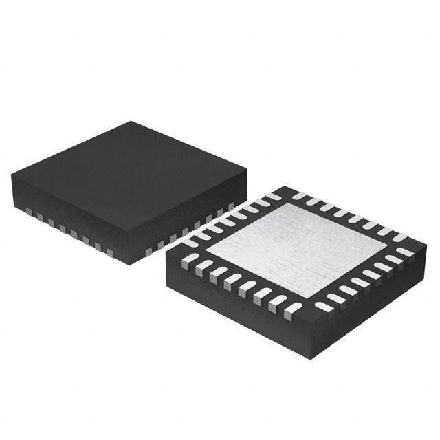
| 产品图片 |
|
| rohs | 符合RoHS无铅 / 符合限制有害物质指令(RoHS)规范要求 |
| 产品系列 | 微控制器 - MCU,8位微控制器 -MCU,Cypress Semiconductor CY8C28243-24PVXIPSOC®1 CY8C28xxx |
| 数据手册 | http://www.cypress.com/?docID=46091 |
| 产品型号 | CY8C28243-24PVXI |
| PCN组件/产地 | http://www.cypress.com/?docID=49128 |
| RAM容量 | 1K x 8 |
| 产品种类 | 8位微控制器 -MCU |
| 供应商器件封装 | 20-SSOP |
| 其它名称 | CY8C2824324PVXI |
| 包装 | 管件 |
| 可编程输入/输出端数量 | 16 |
| 商标 | Cypress Semiconductor |
| 商标名 | PSoC |
| 处理器系列 | CY8C28xxx |
| 外设 | LVD,POR,PWM,WDT |
| 安装风格 | SMD/SMT |
| 宽度 | 7.5 mm |
| 封装 | Tube |
| 封装/外壳 | 20-SSOP(0.209",5.30mm 宽) |
| 封装/箱体 | SSOP-20 |
| 工作温度 | -40°C ~ 85°C |
| 工作电源电压 | 3 V to 5.25 V |
| 工厂包装数量 | 66 |
| 振荡器类型 | 内部 |
| 接口类型 | I2C |
| 数据RAM大小 | 1 kB |
| 数据Ram类型 | SRAM |
| 数据ROM大小 | 16 kB |
| 数据Rom类型 | Flash, EEPROM |
| 数据总线宽度 | 8 bit |
| 数据转换器 | A/D 4x14b; D/A 4x9b |
| 最大工作温度 | + 85 C |
| 最大时钟频率 | 49.2 MHz |
| 最小工作温度 | - 40 C |
| 标准包装 | 66 |
| 核心 | M8C |
| 核心处理器 | M8C |
| 核心尺寸 | 8-位 |
| 片上ADC | Yes |
| 电压-电源(Vcc/Vdd) | 3 V ~ 5.25 V |
| 电源电压-最大 | 5.25 V |
| 电源电压-最小 | 2.4 V |
| 程序存储器大小 | 16 kB |
| 程序存储器类型 | Flash |
| 程序存储容量 | 16KB(16K x 8) |
| 系列 | CY8C28xxx |
| 输入/输出端数量 | 16 I/O |
| 连接性 | I²C, IrDA, SPI, UART/USART |
| 速度 | 24MHz |
| 长度 | 7 mm |
| 高度 | 1.65 mm |


- 商务部:美国ITC正式对集成电路等产品启动337调查
- 曝三星4nm工艺存在良率问题 高通将骁龙8 Gen1或转产台积电
- 太阳诱电将投资9.5亿元在常州建新厂生产MLCC 预计2023年完工
- 英特尔发布欧洲新工厂建设计划 深化IDM 2.0 战略
- 台积电先进制程称霸业界 有大客户加持明年业绩稳了
- 达到5530亿美元!SIA预计今年全球半导体销售额将创下新高
- 英特尔拟将自动驾驶子公司Mobileye上市 估值或超500亿美元
- 三星加码芯片和SET,合并消费电子和移动部门,撤换高东真等 CEO
- 三星电子宣布重大人事变动 还合并消费电子和移动部门
- 海关总署:前11个月进口集成电路产品价值2.52万亿元 增长14.8%


PDF Datasheet 数据手册内容提取
CY8C28243/CY8C28403/CY8C28413 CY8C28433/CY8C28445/CY8C28452 CY8C28513/CY8C28545 CY8C28623/CY8C28643/CY8C28645 ® PSoC Programmable System-on-Chip™ Features ❐Pull-up, pull-down, high Z, strong, or open-drain drive modes on all GPIOs ■Varied resource options within one PSoC® device group ❐Analog input on all GPIOs ❐30 mA analog outputs on GPIOs ■Powerful Harvard-architecture processor ❐Configurable interrupt on all GPIOs ❐M8C processor speeds up to 24 MHz ❐8 × 8 Multiply, 32-bit accumulate ■Additional system resources ❐Low power at high speed ❐Up to two hardware I2C resources ❐Operating voltage: 3.0 V to 5.25 V • Each resource implements slave, master, or multi-master ❐Operating voltages down to 1.5 V Using on-chip switched modes mode pump (SMP) • Operation between 0 and 400 kHz ❐Industrial temperature range: –40 °C to +85 °C ❐Watchdog and Sleep timers ■Advanced reconfigurable peripherals (PSoC Blocks) ❐User-configurable low voltage detection ❐Flexible internal voltage references ❐Up to 12 rail-to-rail analog PSoC blocks provide: ❐Integrated supervisory circuit • Up to 14-bit ADCs ❐On-chip precision voltage reference • Up to 9-bit DACs • Programmable gain amplifiers ■Complete development tools • Programmable filters and comparators ❐Free development software (PSoC Designer™) • Multiple ADC configurations ❐Full featured in-circuit emulator, and programmer ❐Full speed emulation • Dedicated SAR ADC, up to 142 ksps with sample and hold ❐Flexible and functional breakpoint structure • Up to 4 synchronized or independent delta-sigma ADCs for ❐128 KB trace memory advanced applications ❐Up to 4 limited type E analog blocks provide: Logic Block Diagram • Dual channel capacitive sensing capability • Comparators with programmable DAC reference Analog Port 5 Port 4 Port 3 Port 2 Port 1 Port 0 • Up to 10-bit single-slope ADCs Drivers PSoC ❐Up to 12 digital PSoC blocks provide: CORE • 8- to 32-bit timers and counters, 8- and 16-bit pulse-width modulators (PWMs) System Bus • Shift register, CRC, and PRS modules • Up to 3 full-duplex UARTs Global Digital Interconnect Global Analog Interconnect • Up to 6 half-duplex UARTs SRAM • Multiple variable data length SPI masters or slaves 1K SROM Flash 16K CPU Core (M8C) Sleep and • Connectable to all GPIOs Interrupt Watchdog Controller ❐Complex peripherals by combining blocks ■Precision, programmable clocking Multiple Clock Sources (Includes IMO, ILO, PLL, and ECO) ❐Internal ±2.5% 24/48 MHz main oscillator ❐Optional 32.768 kHz crystal for precise on-chip clocks DIGITAL SYSTEM ANALOG SYSTEM ❐Optional external oscillator, up to 24 MHz Analog ❐Internal low speed, low power oscillator for watchdog and Ref. sleep functionality Digital Analog Block Block ■Flexible on-chip memory Array Array Analog ❐16 KB flash program storage 50,000 erase/write cycles Input Muxing ❐1-KB SRAM data storage ❐In-system serial programming (ISSP) ❐Partial flash updates ❐Flexible protection modes ❐EEPROM emulation in flash Digital 2 4 Type 2 2 I2C POR and LVD Internal Switch Voltage Mode Clocks MACs Decimators Blocks System Resets Ref. Pump ■Programmable Pin configurations SYSTEM RESOURCES ❐25 mA sink, 10 mA drive on all GPIOs CypressSemiconductorCorporation • 198 Champion Court • SanJose, CA 95134-1709 • 408-943-2600 Document Number: 001-48111 Rev. *P Revised May 2, 2017
CY8C28243/CY8C28403/CY8C28413 CY8C28433/CY8C28445/CY8C28452 CY8C28513/CY8C28545 CY8C28623/CY8C28643/CY8C28645 Contents More Information ..............................................................3 Thermal Impedances .................................................72 PSoC Designer ..................................................................3 Capacitance on Crystal Pins .....................................72 PSoC Functional Overview ..............................................4 Solder Reflow Specifications .....................................72 The PSoC Core ...........................................................4 Development Tool Selection .........................................73 The Digital System ......................................................4 Software ....................................................................73 The Analog System .....................................................5 Development Kits ......................................................73 System Resources ......................................................8 Evaluation Tools ........................................................73 PSoC Device Characteristics ......................................8 Device Programmers .................................................74 Development Tools ........................................................10 Accessories (Emulation and Programming) ..............74 PSoC Designer Software Subsystems ......................10 Ordering Information ......................................................75 Designing with PSoC Designer .....................................11 Ordering Code Definitions .........................................76 Select User Modules .................................................11 Acronyms ........................................................................77 Configure User Modules ............................................11 Acronyms Used .........................................................77 Organize and Connect ..............................................11 Reference Documents ....................................................77 Generate, Verify, and Debug .....................................11 Document Conventions .................................................78 Pinouts ............................................................................12 Units of Measure .......................................................78 20-pin Part Pinout ......................................................12 Numeric Conventions ................................................78 28-pin Part Pinout ......................................................13 Glossary ..........................................................................78 44-pin Part Pinout ......................................................14 Errata ...............................................................................83 48-pin Part Pinout ......................................................15 Part Numbers Affected ..............................................83 56-pin Part Pinout ......................................................16 Qualification Status ...................................................83 Register Reference .........................................................18 Errata Summary ........................................................83 Register Conventions ................................................18 Document History Page .................................................85 Register Mapping Tables ..........................................18 Sales, Solutions, and Legal Information ......................87 Electrical Specifications ................................................33 Worldwide Sales and Design Support .......................87 Absolute Maximum Ratings .......................................34 Products ....................................................................87 Operating Temperature .............................................34 PSoC® Solutions ......................................................87 DC Electrical Characteristics .....................................35 Cypress Developer Community .................................87 AC Electrical Characteristics .....................................55 Technical Support .....................................................87 Packaging Information ...................................................68 Packaging Dimensions ..............................................68 Document Number: 001-48111 Rev. *P Page 2 of 87
CY8C28243/CY8C28403/CY8C28413 CY8C28433/CY8C28445/CY8C28452 CY8C28513/CY8C28545 CY8C28623/CY8C28643/CY8C28645 More Information Note: For CY8C28xxx devices related Development Kits please click here. Cypress provides a wealth of data at www.cypress.com to help The MiniProg1 and MiniProg3 devices provide interfaces for you to select the right PSoC device for your design, and to help flash programming and debug. you to quickly and effectively integrate the device into your design. For a comprehensive list of resources, see the PSoC Designer knowledge base article “How to Design with PSoC® 1, PowerPSoC®, and PLC – KBA88292”. Following is an PSoC Designer is a free Windows-based Integrated Design abbreviated list for PSoC 1: Environment (IDE). Develop your applications using a library of pre-characterized analog and digital peripherals in a ■Overview: PSoC Portfolio, PSoC Roadmap drag-and-drop design environment. Then, customize your ■Product Selectors: PSoC 1, PSoC 3, PSoC 4, PSoC 5LP design leveraging the dynamically generated API libraries of code. Figure1 shows PSoC Designer windows. Note: This is not ■In addition, PSoC Designer includes a device selection tool. the default view. ■Application notes: Cypress offers a large number of PSoC 1.Global Resources – all device hardware settings. application notes covering a broad range of topics, from basic 2.Parameters – the parameters of the currently selected User to advanced level. Recommended application notes for getting Modules. started with PSoC 1 are: ❐Getting Started with PSoC® 1 – AN75320. 3.Pinout – information related to device pins. ❐PSoC® 1 - Getting Started with GPIO – AN2094. 4.Chip-Level Editor – a diagram of the resources available on ❐PSoC® 1 Analog Structure and Configuration – AN74170. the selected chip. ❐PSoC® 1 Switched Capacitor Analog Blocks – AN2041. 5.Datasheet – the datasheet for the currently selected UM ❐Selecting Analog Ground and Reference – AN2219. 6.User Modules – all available User Modules for the selected device. Note: For CY8C28xxx devices related Application note please click here. 7.Device Resource Meter – device resource usage for the current project configuration. ■Development Kits: 8.Workspace – a tree level diagram of files associated with the ❐CY3210-PSoCEval1 supports all PSoC 1 Mixed-Signal Array project. families, including automotive, except CY8C25/26xxx devices. The kit includes an LCD module, potentiometer, 9.Output – output from project build and debug operations. LEDs, and breadboarding space. Note: For detailed information on PSoC Designer, go to ❐CY3214-PSoCEvalUSB features a development board for PSoC® Designer > Help > Documentation > the CY8C24x94 PSoC device. Special features of the board Designer Specific Documents > IDE User Guide. include USB and CapSense development and debugging support. Figure 1. PSoC Designer Layout Document Number: 001-48111 Rev. *P Page 3 of 87
CY8C28243/CY8C28403/CY8C28413 CY8C28433/CY8C28445/CY8C28452 CY8C28513/CY8C28545 CY8C28623/CY8C28643/CY8C28645 PSoC Functional Overview 32-bit peripherals, which are called user modules. The digital blocks can be connected to any GPIO through a series of global The PSoC family consists of many devices with On-Chip buses that can route any signal to any pin. Controllers. These devices are designed to replace multiple Figure 2. Digital System Block Diagram[1] traditional MCU based system components with one low cost single chip programmable component. A PSoC device includes Port 5 Port 3 Port 1 configurable analog blocks, digital blocks, and interconnections. Port 4 Port 2 Port 0 This architecture enables the user to create customized Digital Clocks To Analog peripheral configurations to match the requirements of each From Core To System Bus System individual application. In addition, a fast CPU, Flash program memory, SRAM data memory, and configurable I/O are included in a range of convenient pinouts and packages. DIGITAL SYSTEM The CY8C28xxx group of PSoC devices described in this Digital PSoC Block Array datasheet have multiple resource configuration options adCdaveYats8acilsCarihbb2ele8eedx.t 4. T5Tis hh seeaurrevbeafg oairlrroaeeub, plsei nx ho fmaot sro e raevee a sfrcuyehl gl rmCfeeesYaon8tuutCerrdec2e 8ss xuexmbtx ge ornsof tuuiaobplngls er rtodehu sapoitn .ua rlTtclohhewiess Row InputConfiguration DBC00 DBC01RowD C0C02 DCC0344 ConfigurationRow Output 8 8 designers to use a device with only the resources and functionality necessary for a specific application. See Table 2 on 8 8 pCinaY mg8eoC r2e98 d xexttxoa isl udinbe gttehroremu Opin.r edT ehretinh gesa Imnrfeeos rimonufaortcriomensa stieoacnvta iiosilna a.bllseo pforer seenatechd Row InputConfiguration DBC10 DBC11RowD C1C12 DCC1344 ConfigurationRow Output The architecture for this specific PSoC device family, as shown in the Logic Block Diagram on page 1, consists of four main aRdsyreeesvsatieocsemu: rP.c rSeePsosS.oC oTu CCrhc eoeC rsecY o,8 tnDoCfi ig2gbi8uteaxr alx bSxcl oyefmsa tgmbelimoinlbye, adAdl nebiavnulitocsoge s sSay syhtscaetovmemem pau, llpaelo ntewtdo s Sc sauyixlssl ttoteIh/mmOe Row InputConfiguration DBC20 DBC21RowD C2C22 DCC2344 ConfigurationRow Output ports that connect to the global digital and analog interconnects, providing access to up to 12 digital blocks and up to 16 analog GIE[7:0] Global Digital GOE[7:0] blocks. GIO[7:0] Interconnect GOO[7:0] The PSoC Core The PSoC Core is a powerful engine that supports a rich feature Digital peripheral configurations include: set. The core includes a CPU, memory, clocks, and configurable general Purpose I/O (GPIO). The M8C CPU core is a powerful ■PWMs (8- and 16-bit, One-shot and Multi-shot capability) processor with speeds up to 24 MHz, providing a four MIPS 8-bit ■PWMs with Dead band/Kill (8- and 16-bit) Harvard architecture microcontroller. Memory encompasses 16K bytes of Flash for program storage, ■Counters (8 to 32 bit) 1K bytes of SRAM for data storage. The PSoC device incorpo- ■Timers (8 to 32 bit) rates flexible internal clock generators, including a 24 MHz internal main oscillator (IMO) accurate to 2.5% over temperature ■Full-duplex 8-bit UARTs (up to 3) with selectable parity and voltage. A low power 32 kHz internal low speed oscillator ■Half-duplex 8-bit UARTs (up to 6) with selectable parity (ILO) is provided for the sleep timer and watch dog timer (WDT). The 32.768 kHz external crystal oscillator (ECO) is available for ■Variable length SPI slave and master use as a real time clock (RTC) and can optionally generate a ❐Up to 6 total slaves and masters (8-bit) crystal-accurate 24 MHz system clock using a PLL. ❐Supports 8 to 16 bit operation PSoC GPIOs provide connections to the CPU, and digital and ■I2C slave, master, or multi-master (up to 2 available as System analog resources. Each pin’s drive mode may be selected from Resources) 8 options, which allows great flexibility in external interfacing. Every pin also has the capability to generate a system interrupt ■IrDA (up to 3) on high level, low level, and change from last read. ■Pseudo Random Sequence Generators (8 to 32 bit) The Digital System ■Cyclical Redundancy Checker/Generator (16 bit) The Digital System is composed of up to 12 configurable digital ■Shift Register (2 to 32 bit) PSoC blocks. Each block is an 8-bit resource that can be used alone or combined with other blocks to create 8, 16, 24, and Note 1. CY8C28x52 devices do not have digital block row 2. They have two digital rows with eight total digital blocks. Document Number: 001-48111 Rev. *P Page 4 of 87
CY8C28243/CY8C28403/CY8C28413 CY8C28433/CY8C28445/CY8C28452 CY8C28513/CY8C28545 CY8C28623/CY8C28643/CY8C28645 The Analog System Figure 3. Analog System Block Diagram for CY8C28x45 and CY8C28x52 Devices The Analog System is composed of up to 16 configurable analog blocks, each containing an opamp circuit that allows the creation All GPIO of complex analog signal flows. Some devices in this PSoC family have an analog multiplex bus that can connect to every P0[7] P0[6] GPIO pin. This bus can also connect to the analog system for P0[5] P0[4] analysis with comparators and analog-to-digital converters. It can be split into two sections for simultaneous dual-channel P0[3] P0[2] processing. P0[1] P0[0] Savoamilae bloef atsh eu semr omreo dcuolemsm) aorne :PSoC analog functions (most RefIn P2[6] P2[3] DIn ■Analog-to-digital converters (6 to 14-bit resolution, up to 4, N P2[4] G ■sDeeledicctaatbeled a1s0 -Ibnict rSeAmRe nAtDalC o rw Dithe ltsaa mSipglme ara)tes up to 142 ksps P2[1] Analog Mux Bus A PP22[[20]] ■Synchronized, simultaneous Delta Sigma ADCs (up to 4) ■Filters (2 to 8 pole band-pass, low pass, and notch) Array Input Configuration ■Amplifiers (up to 4, with selectable gain to 48x) ■Instrumentation amplifiers (up to 2, with selectable gain to 93x) ACI0[1:0] ACI1[1:0] ACI2[1:0] ACI3[1:0] ACI4[1:0] ACI5[1:0] ■Comparators (up to 6, with 16 selectable thresholds) ■DACs (up to 4, with 6 to 9-bit resolution) Block Array ■Multiplying DACs (up to 4, with 6 to 9-bit resolution) ACC00 ACC01 ACC02 ACC03 ACE00 ACE01 ■High current output drivers (up to 4 with 30 mA drive) ASC10 ASD11 ASC12 ASD13 ASE10 ASE11 ■1.3 V reference (as a System Resource) ASD20 ASC21 ASD22 ASC23 ■DTMF Dialer ■Modulators Analog Reference ■Correlators Interface to RefHi Reference AGNDIn Digital System RefLo Generators RefIn ■Peak detectors AGND Bandgap ■Many other topologies possible M8C Interface (Address Bus, Data Bus, Etc.) Document Number: 001-48111 Rev. *P Page 5 of 87
CY8C28243/CY8C28403/CY8C28413 CY8C28433/CY8C28445/CY8C28452 CY8C28513/CY8C28545 CY8C28623/CY8C28643/CY8C28645 Figure 4. Analog System Block Diagram for CY8C28x43 Figure 5. Analog System Block Diagram for CY8C28x33 Devices Devices All GPIO All GPIO P0[7] P0[6] P0[7] P0[5] P0[4] P0[5] P0[6] P0[3] P0[2] P0[3] P0[4] P0[1] P0[0] P0[1] efIn P2[6] P2[3] P0[2] R PP22[[31]] Analog Mux Bus AGNDIn PPP222[[[204]]] P2[1] Analog Mux Bus RefInGNDIn PPP022[[[064]]] A Array Input Configuration Array Input Configuration ACI0[1:0] ACI1[1:0] ACI4[1:0] ACI5[1:0] ACI0[1:0] ACI1[1:0] ACI2[1:0] ACI3[1:0] Block Array ACC00 ACC01 Block Array ACE00 ACE01 ACC00 ACC01 ACC02 ACC03 ASC10 ASD11 ASE10 ASE11 ASC10 ASD11 ASC12 ASD13 ASD20 ASC21 ASD20 ASC21 ASD22 ASC23 Analog Reference Analog Reference Interface to RefHi Reference AGNDIn Digital System RefLo Generators RefIn AGND Bandgap Interface to RefHi Reference AGNDIn Digital System RefLo Generators RefIn AGND Bandgap M8C Interface (Address Bus, Data Bus, Etc.) M8C Interface (Address Bus, Data Bus, Etc.) Document Number: 001-48111 Rev. *P Page 6 of 87
CY8C28243/CY8C28403/CY8C28413 CY8C28433/CY8C28445/CY8C28452 CY8C28513/CY8C28545 CY8C28623/CY8C28643/CY8C28645 Figure 6. Analog System Block Diagram for CY8C28x23 Figure 7. Analog System Block Diagram for CY8C28x13 Devices Devices P0[7] All GPIO P0[5] P0[6] P0[7] ux P0[6] PP00[[31]] P0[4] P0[5] Analog MBus P0[4] P0[2] P2[3] P0[3] P0[2] P0[0] P2[1] P0[1] P0[0] n efI P2[6] R n DI N P2[4] Array Input G A Configuration ACI0[1:0] ACI1[1:0] Array Input Configuration ACI0[1:0] ACI1[1:0] Block Array ACE00 ACE01 Block Array ASE10 ASE11 ACC00 ACC01 Analog Reference ASC10 ASD11 ASD20 ASC21 Interface to RefHi Reference AGNDIn Digital System RefLo Generators RefIn AGND Bandgap Analog Reference M8C Interface (Address Bus, Data Bus, Etc.) Interface to RefHi Reference AGNDIn Digital System RefLo Generators RefIn AGND Bandgap M8C Interface (Address Bus, Data Bus, Etc.) Document Number: 001-48111 Rev. *P Page 7 of 87
CY8C28243/CY8C28403/CY8C28413 CY8C28433/CY8C28445/CY8C28452 CY8C28513/CY8C28545 CY8C28623/CY8C28643/CY8C28645 System Resources ■Up to four decimators provide custom hardware filters for digital signal processing applications such as Delta-Sigma ADCs and System Resources, some of which are listed in the previous CapSense capacitive sensor measurement. sections, provide additional capability useful to complete systems. Additional resources include a multiplier, multiple ■Up to two I2C resources provide 0 to 400 kHz communication decimators, switch mode pump, low voltage detection, and over two wires. Slave, master, and multi-master modes are all power on reset. Statements describing the merits of each system supported. I2C resources have hardware address detection resource follow: capability. ■Digital clock dividers provide three customizable clock ■Low Voltage Detection (LVD) interrupts can signal the appli- frequencies for use in applications. The clocks can be routed cation of falling voltage levels, while the advanced POR (Power to both the digital and analog systems. Additional clocks can On Reset) circuit eliminates the need for a system supervisor. be generated using digital PSoC blocks as clock dividers. ■An internal 1.3 V reference provides an absolute reference for ■Multiply accumulate (MAC) provides fast 8-bit multiplier with the analog system, including ADCs and DACs. 32-bit accumulate, to assist in general math and digital filters. ■An integrated switch mode pump (SMP) generates normal operating voltages from a single 1.5 V battery cell, providing a low cost boost converter. PSoC Device Characteristics Depending on your PSoC device characteristics, the digital and analog systems can have 16, 8, or 4 digital blocks, and 12, 6, or 4 analog blocks. Table1 lists the resources available for specific PSoC device groups. The PSoC device covered by this datasheet is highlighted in this table. Table 1. PSoC Device Characteristics PSoC Part Digital Digital Digital Analog Analog Analog Analog SRAM Flash Number I/O Rows Blocks Inputs Outputs Columns Blocks Size Size CY8C29x66 up to 64 4 16 up to 12 4 4 12 2 K 32 K CY8C28xxx up to 44 up to 3 up to 12 up to 44 up to 4 up to 6 up to 1 K 16 K 12 + 4[2] CY8C27x43 up to 44 2 8 up to 12 4 4 12 256 16 K CY8C24x94 up to 56 1 4 up to 48 2 2 6 1 K 16 K CY8C24x23A up to 24 1 4 up to 12 2 2 6 256 4 K CY8C23x33 up to 26 1 4 up to 12 2 2 4 256 8 K CY8C22x45 up to 38 2 8 up to 38 0 4 6[2] 1 K 16 K CY8C21x45 up to 24 1 4 up to 24 0 4 6[2] 512 8 K CY8C21x34 up to 28 1 4 up to 28 0 2 4[2] 512 8 K CY8C21x23 up to 16 1 4 up to 8 0 2 4[2] 256 4 K CY8C20x34 up to 28 0 0 up to 28 0 0 3[2,3] 512 8 K CY8C20xx6 up to 36 0 0 up to 36 0 0 3[2,3] up to 2 K up to 32 K Notes 2. Limited analog functionality. 3. Two analog blocks and one CapSense®. Document Number: 001-48111 Rev. *P Page 8 of 87
CY8C28243/CY8C28403/CY8C28413 CY8C28433/CY8C28445/CY8C28452 CY8C28513/CY8C28545 CY8C28623/CY8C28643/CY8C28645 The devices covered by this datasheet all have the same architecture, specifications, and ratings. However, the amount of some hardware resources varies from device to device within the group. The following table lists resources available for the specific device subgroups covered by this datasheet. Table 2. CY8C28xxx Device Characteristics Regular Limited Analog PSoC Part CapSense Digital Analog Analog HW I2C Decimators Digital Analog Analog Mux Number Blocks I/O Inputs Outputs Blocks Blocks Buses CY8C28x03 N 12 0 0 2 0 up to 24 up to 8 0 0 CY8C28x13 Y 12 0 4 1 2 up to 40 up to 40 0 2 CY8C28x23 N 12 6 0 2 2 up to 44 up to 10 2 0 CY8C28x33 Y 12 6 4 1 4 up to 40 up to 40 2 2 CY8C28x43 N 12 12 0 2 4 up to 44 up to 44 4 2 CY8C28x45 Y 12 12 4 2 4 up to 44 up to 44 4 2 CY8C28x52 Y 8 12 4 1 4 up to 24 up to 24 4 2 Document Number: 001-48111 Rev. *P Page 9 of 87
CY8C28243/CY8C28403/CY8C28413 CY8C28433/CY8C28445/CY8C28452 CY8C28513/CY8C28545 CY8C28623/CY8C28643/CY8C28645 Development Tools time. In essence, this lets you to use more than 100 percent of PSoC’s resources for an application. PSoC Designer™ is the revolutionary integrated design environment (IDE) that you can use to customize PSoC to meet Code Generation Tools your specific application requirements. PSoC Designer software The code generation tools work seamlessly within the accelerates system design and time to market. Develop your PSoCDesigner interface and have been tested with a full range applications using a library of precharacterized analog and digital of debugging tools. You can develop your design in C, assembly, peripherals (called user modules) in a drag-and-drop design or a combination of the two. environment. Then, customize your design by leveraging the dynamically generated application programming interface (API) Assemblers. The assemblers allow you to merge assembly libraries of code. Finally, debug and test your designs with the code seamlessly with C code. Link libraries automatically use integrated debug environment, including in-circuit emulation and absolute addressing or are compiled in relative mode, and linked standard software debug features. PSoC Designer includes: with other software modules to get absolute addressing. C Language Compilers. C language compilers are available ■Application editor graphical user interface (GUI) for device and that support the PSoC family of devices. The products allow you user module configuration and dynamic reconfiguration to create complete C programs for the PSoC family devices. The ■Extensive user module catalog optimizing C compilers provide all of the features of C, tailored to the PSoC architecture. They come complete with embedded ■Integrated source-code editor (C and assembly) libraries providing port and bus operations, standard keypad and ■Free C compiler with no size restrictions or time limits display support, and extended math functionality. ■Built-in debugger Debugger ■In-circuit emulation PSoC Designer has a debug environment that provides hardware in-circuit emulation, allowing you to test the program in ■Built-in support for communication interfaces: a physical system while providing an internal view of the PSoC ❐Hardware and software I2C slaves and masters device. Debugger commands allow you to read and program and ❐Full-speed USB 2.0 read and write data memory, and read and write I/O registers. ❐Up to four full-duplex universal asynchronous You can read and write CPU registers, set and clear breakpoints, receiver/transmitters (UARTs), SPI master and slave, and and provide program run, halt, and step control. The debugger wireless also lets you to create a trace buffer of registers and memory locations of interest. PSoC Designer supports the entire library of PSoC 1 devices and runs on Windows XP, Windows Vista, and Windows 7. Online Help System PSoC Designer Software Subsystems The online help system displays online, context-sensitive help. Designed for procedural and quick reference, each functional Design Entry subsystem has its own context-sensitive help. This system also In the chip-level view, choose a base device to work with. Then provides tutorials and links to FAQs and an Online Support select different onboard analog and digital components that use Forum to aid the designer. the PSoC blocks, which are called user modules. Examples of In-Circuit Emulator user modules are analog-to-digital converters (ADCs), digital-to-analog converters (DACs), amplifiers, and filters. A low-cost, high-functionality in-circuit emulator (ICE) is Configure the user modules for your chosen application and available for development support. This hardware can program connect them to each other and to the proper pins. Then single devices. generate your project. This prepopulates your project with APIs The emulator consists of a base unit that connects to the PC and libraries that you can use to program your application. using a USB port. The base unit is universal and operates with The tool also supports easy development of multiple all PSoC devices. Emulation pods for each device family are configurations and dynamic reconfiguration. Dynamic available separately. The emulation pod takes the place of the reconfiguration makes it possible to change configurations at run PSoC device in the target board and performs full-speed (24MHz) operation. Document Number: 001-48111 Rev. *P Page 10 of 87
CY8C28243/CY8C28403/CY8C28413 CY8C28433/CY8C28445/CY8C28452 CY8C28513/CY8C28545 CY8C28623/CY8C28643/CY8C28645 Designing with PSoC Designer specifications. Each datasheet describes the use of each user module parameter, and other information that you may need to The development process for the PSoC device differs from that successfully implement your design. of a traditional fixed-function microprocessor. The configurable analog and digital hardware blocks give the PSoC architecture a Organize and Connect unique flexibility that pays dividends in managing specification Build signal chains at the chip level by interconnecting user change during development and lowering inventory costs. These modules to each other and the I/O pins. Perform the selection, configurable resources, called PSoC blocks, have the ability to configuration, and routing so that you have complete control over implement a wide variety of user-selectable functions. The PSoC all on-chip resources. development process is: 1.Select user modules. Generate, Verify, and Debug 2.Configure user modules. When you are ready to test the hardware configuration or move 3.Organize and connect. on to developing code for the project, perform the “Generate Configuration Files” step. This causes PSoC Designer to 4.Generate, verify, and debug. generate source code that automatically configures the device to Select User Modules your specification and provides the software for the system. The generated code provides APIs with high-level functions to control PSoC Designer provides a library of prebuilt, pretested hardware and respond to hardware events at run time, and interrupt peripheral components called “user modules.” User modules service routines that you can adapt as needed. make selecting and implementing peripheral devices, both A complete code development environment lets you to develop analog and digital, simple. and customize your applications in C, assembly language, or Configure User Modules both. Each user module that you select establishes the basic register The last step in the development process takes place inside settings that implement the selected function. They also provide PSoC Designer's Debugger (accessed by clicking the Connect parameters and properties that allow you to tailor their precise icon). PSoC Designer downloads the HEX image to the ICE configuration to your particular application. For example, a PWM where it runs at full-speed. PSoC Designer debugging User Module configures one or more digital PSoC blocks, one capabilities rival those of systems costing many times more. In for each eight bits of resolution. Using these parameters, you can addition to traditional single-step, run-to-breakpoint, and establish the pulse width and duty cycle. Configure the watch-variable features, the debug interface provides a large parameters and properties to correspond to your chosen trace buffer. It lets you to define complex breakpoint events that application. Enter values directly or by selecting values from include monitoring address and data bus values, memory drop-down menus. All of the user modules are documented in locations, and external signals. datasheets that may be viewed directly in PSoCDesigner or on the Cypress website. These user module datasheets explain the internal operation of the user module and provide performance Document Number: 001-48111 Rev. *P Page 11 of 87
CY8C28243/CY8C28403/CY8C28413 CY8C28433/CY8C28445/CY8C28452 CY8C28513/CY8C28545 CY8C28623/CY8C28643/CY8C28645 Pinouts This section describes, lists, and illustrates the CY8C28xxx PSoC device pins and pinout configurations. The CY8C28xxx PSoC devices are available in a variety of packages which are listed and illustrated in the following tables. Every port pin (labeled with a “P”) is capable of Digital I/O. However, V , V , SMP, and XRES are not capable of Digital I/O. SS DD 20-pin Part Pinout Table 3. 20-pin Part Pinout (SSOP) Pin Type Pin CY8C28243 20-pin PSoC Device Description No. Digital Analog Name 1 I/O I, M, S P0[7] Analog column mux and SAR ADC S, AI, M, P0[7] 1 20 Vdd input.[5] S, AIO, M, P0[5] 2 19 P0[6], M, AI, S 2 I/O I/O, M, S P0[5] Analog column mux and SAR ADC input. S, AIO, M, P0[3] 3 18 P0[4], M, AIO, S Analog column output.[5, 6] S, AI, M, P0[1] 4 17 P0[2], M, AIO, S 3 I/O I/O, M, S P0[3] AAnnaalloogg ccoolluummnn mouutxp aunt.d[5 ,S 6A]R ADC input. I2C0 SCL, M, PS1M[7P] 56 SSOP 1165 PXR0[E0]S, M, AI, S 4 I/O I, M, S P0[1] Analog column mux and SAR ADC I2C0 SDA, M, P1[5] 7 14 P1[6], M, I2C1 SCL input.[5] M, P1[3] 8 13 P1[4], M, EXTCLK 5 Output SMP Switch Mode Pump (SMP) connection to I2C0 SCL, XTALin, M, P1[1] 9 12 P1[2], M, I2C1 SDA external components. Vss 10 11 P1[0], M, XTALout, I2C0 SDA 6 I/O M P1[7] I2C0 Serial Clock (SCL). 7 I/O M P1[5] I2C0 Serial Data (SDA). 8 I/O M P1[3] 9 I/O M P1[1] Crystal Input (XTALin), I2C0 Serial Clock (SCL), ISSP-SCLK[4]. 10 Power V Ground connection. SS 11 I/O M P1[0] Crystal Output (XTALout), I2C0 Serial Data (SDA), ISSP-SDATA[4]. 12 I/O M P1[2] I2C1 Serial Data (SDA).[7] 13 I/O M P1[4] Optional External Clock Input (EXTCLK). 14 I/O M P1[6] I2C1 Serial Clock (SCL).[7] 15 Input XRES Active high external reset with internal pull-down. 16 I/O I, M, S P0[0] Analog column mux and SAR ADC input.[5] 17 I/O I/O, M, S P0[2] Analog column mux and SAR ADC input. Analog column output.[5, 8] 18 I/O I/O, M, S P0[4] Analog column mux and SAR ADC input. Analog column output.[5, 8] 19 I/O I, M, S P0[6] Analog column mux and SAR ADC input.[5] 20 Power V Supply voltage. DD LEGEND: A = Analog, I = Input, O = Output, S = SAR ADC Input, and M = Analog Mux Bus Input. Notes 4. These are the ISSP pins, which are not High Z at POR (Power On Reset). See the PSoC Technical Reference Manual for CY8C28xxx PSoC devices for details. 5. CY8C28x52 and CY8C28x23 devices do not have a SAR ADC. Therefore, this pin does not function as a SAR ADC input for these devices. 6. CY8C28x13 and CY8C28x03 devices do not have any analog output buffers. Therefore, this pin does not function as an analog column output for these devices. 7. CY8C28x52, CY8C28x13, and CY8C28x33 devices only have one I2C block. Therefore, this GPIO does not function as an I2C pin for these devices. 8. CY8C28x33, CY8C28x23, CY8C28x13, and CY8C28x03 devices do not have an analog output buffer for this pin. Therefore, this pin does not function as an analog column output for these devices. Document Number: 001-48111 Rev. *P Page 12 of 87
CY8C28243/CY8C28403/CY8C28413 CY8C28433/CY8C28445/CY8C28452 CY8C28513/CY8C28545 CY8C28623/CY8C28643/CY8C28645 28-pin Part Pinout Table 4. 28-pin Part Pinout (SSOP) Pin Type Pin CY8C28403, CY8C28413, CY8C28433, CY8C28445, and Description No. Digital Analog Name CY8C28452 28-pin PSoC Devices 1 I/O I, M, S P0[7] Analog column mux and SAR ADC input.[5] S, AI, M, P0[7] 1 28 Vdd 2 I/O I/O, M, S P0[5] Analog column mux and SAR ADC input. Analog column output.[5, 6] S, AIO, M, P0[5] 2 27 P0[6], M, AI, S S, AIO, M, P0[3] 3 26 P0[4], M, AIO, S 3 I/O I/O, M, S P0[3] Analog column mux and SAR ADC input. Analog column output.[5, 6] S, AI, M, P0[1] 4 25 P0[2], M, AIO, S M, P2[7] 5 24 P0[0], M, AI, S 4 I/O I, M, S P0[1] Analog column mux and SAR ADC input.[5] M, P2[5] 6 23 P2[6], M, External VRef AI, M, P2[3] 7 SSOP 22 P2[4], M, External AGND 5 I/O M P2[7] AI, M, P2[1] 8 21 P2[2], M, AI 6 I/O M P2[5] SMP 9 20 P2[0], M, AI 7 I/O I, M P2[3] Direct switched capacitor block input.[9] I2C0 SCL, M, P1[7] 10 19 XRES 8 I/O I, M P2[1] Direct switched capacitor block input.[9] I2C0 SDA, M, P1[5] 11 18 P1[6], M, I2C1 SCL M, P1[3] 12 17 P1[4], M, EXTCLK 9 Output SMP Switch Mode Pump (SMP) connection to external components. I2C0 SCL, XTALin, M, P1[1] 13 16 P1[2], M, I2C1 SDA Vss 14 15 P1[0], M, XTALout, I2C0 SDA 10 I/O M P1[7] I2C0 Serial Clock (SCL). 11 I/O M P1[5] I2C0 Serial Data (SDA). 12 I/O M P1[3] 13 I/O M P1[1] Crystal Input (XTALin), I2C0 Serial Clock (SCL), ISSP-SCLK[4]. 14 Power V Ground connection. SS 15 I/O M P1[0] Crystal Output (XTALout), I2C0 Serial Data (SDA), ISSP-SDATA[4]. 16 I/O M P1[2] I2C1 Serial Data (SDA).[7] 17 I/O M P1[4] Optional External Clock Input (EXTCLK). 18 I/O M P1[6] I2C1 Serial Clock (SCL).[7] 19 Input XRES Active high external reset with internal pull-down. 20 I/O I, M P2[0] Direct switched capacitor block input.[10] 21 I/O I, M P2[2] Direct switched capacitor block input.[10] 22 I/O M P2[4] External Analog Ground (AGND). 23 I/O M P2[6] External Voltage Reference (VRef). 24 I/O I, M, S P0[0] Analog column mux and SAR ADC input.[5] 25 I/O I/O, M, S P0[2] Analog column mux and SAR ADC input. Analog column output.[5, 8] 26 I/O I/O, M, S P0[4] Analog column mux and SAR ADC input. Analog column output.[5, 8] 27 I/O I, M, S P0[6] Analog column mux and SAR ADC input.[5] 28 Power V Supply voltage. DD LEGEND: A = Analog, I = Input, O = Output, S = SAR ADC Input, and M = Analog Mux Bus Input Notes 9. This pin is not a direct switched capacitor block analog input for CY8C28x03 and CY8C28x13 devices. 10.This pin is not a direct switched capacitor block analog input for CY8C28x03, CY8C28x13, CY8C28x23, and CY8C28x33 devices. Document Number: 001-48111 Rev. *P Page 13 of 87
CY8C28243/CY8C28403/CY8C28413 CY8C28433/CY8C28445/CY8C28452 CY8C28513/CY8C28545 CY8C28623/CY8C28643/CY8C28645 44-pin Part Pinout Table 5. 44-pin Part Pinout (TQFP) Pin Type Pin CY8C28513, and CY8C28545 No. Digital Analog Name Description 44-pin PSoC Devices 1 I/O M P2[5] ef 2 I/O I, M P2[3] Direct switched capacitor block input.[9] VR 3 I/O I, M P2[1] Direct switched capacitor block input.[9] SS SS nal 4 I/O M P4[7] AI, SAIO, AIO, AI, S AI, SAIO, AIO, AI, SExter 5 I/O M P4[5] MM, M, M, M, M, M, M, M, M, 6 I/O M P4[3] 2[7], 0[1], 0[3], 0[5], 0[7], dd0[6], 0[4], 0[2], 0[0], 2[6], 7 I/O M P4[1] PPPPPVPPPPP 8 Output SMP Switch Mode Pump (SMP) connection to 4443424140393837363534 external components. M, P2[5] 1 33 P2[4], M, External AGND 9 I/O M P3[7] AI, M, P2[3] 2 32 P2[2], M, AI AI, M, P2[1] 3 31 P2[0], M, AI 10 I/O M P3[5] M, P4[7] 4 30 P4[6], M 11 I/O M P3[3] M, P4[5] 5 29 P4[4], M 12 I/O M P3[1] M, P4[3] 6 TQFP 28 P4[2], M M, P4[1] 7 27 P4[0], M 13 I/O M P1[7] I2C0 Serial Clock (SCL). SMP 8 26 XRES 14 I/O M P1[5] I2C0 Serial Data (SDA). M, P3[7] 9 25 P3[6], M 15 I/O M P1[3] M, P3[5] 10 24 P3[4], M 16 I/O M P1[1] Crystal Input (XTALin), I2C0 Serial Clock M, P3[3] 11 23 P3[2], M, I2C1 SCL (SCL), ISSP-SCLK[4]. 1213141516171819202122 17 Power VSS Ground connection. 3[1]1[7]1[5]1[3]1[1]Vss1[0]1[2]1[4]1[6]3[0] 18 I/O M P1[0] (CSrDysAta),l IOSuStpPu-St (DXATTAAL[o4]u.t), I2C0 Serial Data M, PM, PM, PM, PM, P M, PM, PM, PM, PM, P 19 I/O M P1[2] I2C1 Serial Data (SDA).[7] SCL, SDA, ALin, Lout, SDA, CLK, SCL, SDA, 2201 II//OO MM PP11[[64]] IO2pCt1io Snaelr iEaxl tCelroncakl C(SloCcLk) .I[n7]put (EXTCLK). I2C0 I2C0 CL, XT A, XTAI2C1 EXTI2C1 I2C1 2223 II//OO MM PP33[[20]] II22CC11 SSeerriiaall CDlaotcak ( S(SDCAL))..[7[7]] 2C0 S C0 SD I 2 24 I/O M P3[4] I 25 I/O M P3[6] 26 Input XRES Active high external reset with internal pull-down. 27 I/O M P4[0] 28 I/O M P4[2] 29 I/O M P4[4] 30 I/O M P4[6] 31 I/O I, M P2[0] Direct switched capacitor block input.[10] 32 I/O I, M P2[2] Direct switched capacitor block input.[10] 33 I/O M P2[4] External Analog Ground (AGND). 34 I/O M P2[6] External Voltage Reference (VRef). 35 I/O I, M, S P0[0] Analog column mux and SAR ADC input.[5] 36 I/O I/O, M S P0[2] Analog column mux and SAR ADC input. Analog column output.[5, 8] 37 I/O I/O, M, S P0[4] Analog column mux and SAR ADC input. Analog column output.[5, 8] 38 I/O I, M, S P0[6] Analog column mux and SAR ADC input.[5] 39 Power V Supply voltage. DD 40 I/O I, M, S P0[7] Analog column mux and SAR ADC input.[5] 41 I/O I/O, M, S P0[5] Analog column mux and SAR ADC input. Analog column output.[5, 6] 42 I/O I/O, M, S P0[3] Analog column mux and SAR ADC input. Analog column output.[5, 6] 43 I/O I, M, S P0[1] Analog column mux and SAR ADC input.[5] 44 I/O P2[7] LEGEND: A = Analog, I = Input, O = Output, S = SAR ADC Input, and M = Analog Mux Bus Input. Document Number: 001-48111 Rev. *P Page 14 of 87
CY8C28243/CY8C28403/CY8C28413 CY8C28433/CY8C28445/CY8C28452 CY8C28513/CY8C28545 CY8C28623/CY8C28643/CY8C28645 48-pin Part Pinout Table 6. 48-pin Part Pinout (QFN[11]) Pin Type Pin CY8C28623, CY8C28643, and CY8C28645 No. Digital Analog Name Description 48-pin PSoC Devices 1 I/O I, M P2[3] Direct switched capacitor block input.[9] ef R 234 III///OOO I,MM M PPP442[[[751]]] Direct switched capacitor block input.[9] MMM, AI, SM, AIO, SM, AIO, SM, AI, S M, AI, SM, AIO, SM, AIO, SM, AI, SM, External V 56 II//OO MM PP44[[31]] P2[5], P2[7], P0[1], P0[3], P0[5], P0[7], VddP0[6], P0[4], P0[2], P0[0], P2[6], 7 Output SMP Sexwteitcrnha Ml coodme pPounmepn t(sS.MP) connection to AI, M, P2[3] 1 48474645444342414039383736 P2[4], M, External AGND AI, M, P2[1] 2 35 P2[2], M, AI 8 I/O M P3[7] M, P4[7] 3 34 P2[0], M, AI 9 I/O M P3[5] M, P4[5] 4 33 P4[6], M 10 I/O M P3[3] M, P4[3] 5 32 P4[4], M 11 I/O M P3[1] M, P4[1] 6 QFN 31 P4[2], M SMP 7 (Top View) 30 P4[0], M 12 I/O M P5[3] M, P3[7] 8 29 XRES 13 I/O M P5[1] M, P3[5] 9 28 P3[6], M 14 I/O M P1[7] I2C0 Serial Clock (SCL). M, P3[3] 10 27 P3[4], M 15 I/O M P1[5] I2C0 Serial Data (SDA). M, P3[1] 11 26 P3[2], M, I2C1 SCL M, P5[3] 12 25 P3[0], M, I2C1 SDA 16 I/O M P1[3] 345678901234 111111122222 17 I/O M P1[1] Crystal Input (XTALin), I2C0 Serial Clock (SCL), ISSP-SCLK[4]. 5[1]1[7]1[5]1[3]1[1]Vss1[0]1[2]1[4]1[6]5[0]5[2] PPPPP PPPPPP 112890 II//OOPowerMM PPV11S[[S02]] GDCI2arrCyotas1ut na(SSdle DOcriAouantl) p,nD uIeSatc tS(atXiPo (Tn-SAS.DLDAoAu)T.t[A)7,] [4I2].C0 Serial M, I2C0 SCL, M, I2C0 SDA, M, M, CL, XTALin, M, A, XTALout, M, I2C1 SDA, M, EXTCLK, M, I2C1 SCL, M, M, M, S D 21 I/O M P1[4] (OEpXtiToCnaLlK E).xternal Clock Input 2C0 C0 S I 2 22 I/O M P1[6] I2C1 Serial Clock (SCL).[7] I 23 I/O M P5[0] 24 I/O M P5[2] 25 I/O M P3[0] I2C1 Serial Data (SDA).[7] 26 I/O M P3[2] I2C1 Serial Clock (SCL).[7] 27 I/O M P3[4] 28 I/O M P3[6] 29 Input XRES Active high external reset with internal pull-down. 30 I/O M P4[0] 31 I/O M P4[2] Type Pin Pin 32 I/O M P4[4] No. Digital Analog Naem Description 33 I/O M P4[6] 41 I/O I, M, S P0[6] Analog column mux and SAR ADC input.[5] 34 I/O I, M P2[0] Direct switched capacitor block input.[10] 42 Power V Supply voltage. DD 35 I/O I, M P2[2] Direct switched capacitor block input.[10] 43 I/O I, M, S P0[7] Analog column mux and SAR ADC input.[5] 36 I/O M P2[4] External Analog Ground (AGND). 44 I/O I/O, M, S P0[5] Analog column mux and SAR ADC input. Analog column output.[5, 6] 37 I/O M P2[6] External Voltage Reference (VRef). 45 I/O I/O, M, S P0[3] Analog column mux and SAR ADC input. Analog column output.[5, 6] 38 I/O I, M, S P0[0] Analog column mux and SAR ADC 46 I/O I, M, S P0[1] Analog column mux and SAR ADC input.[5] input.[5] 39 I/O I/O, M, S P0[2] Analog column mux and SAR ADC input. 47 I/O M P2[7] Analog column output.[5, 8] 40 I/O I/O, M, S P0[4] Analog column mux and SAR ADC input. 48 I/O M P2[5] Analog column output.[5, 8] LEGEND: A = Analog, I = Input, O = Output, S = SAR ADC Input, and M = Analog Mux Bus Input. Note 11.The QFN package has a center pad that must be connected to ground (VSS) Document Number: 001-48111 Rev. *P Page 15 of 87
CY8C28243/CY8C28403/CY8C28413 CY8C28433/CY8C28445/CY8C28452 CY8C28513/CY8C28545 CY8C28623/CY8C28643/CY8C28645 56-pin Part Pinout The 56-pin SSOP part is for the CY8C28000 On-Chip Debug (OCD) PSoC device. Note This part is only used for in-circuit debugging. It is NOT available for production. Table 7. 56-pin Part Pinout (SSOP) Pin Type Pin CY8C28000 56-pin PSoC Device Description No. Digital Analog Name 1 NC No connection. NC 1 56 Vdd 2 I/O I, M, S P0[7] Analog column mux and SAR ADC input. S, AI, M, P0[7] 2 55 P0[6], M, AI, S S, AIO, M, P0[5] 3 54 P0[4], M, AIO, S 3 I/O I/O, M, S P0[5] Analog column mux and SAR ADC input. S, AIO, M, P0[3] 4 53 P0[2], M, AIO, S Analog column output. S, AI, M, P0[1] 5 52 P0[0], M, AI, S M, P2[7] 6 51 P2[6], M, External VRef 4 I/O I/O, M, S P0[3] Analog column mux and SAR ADC input. M, P2[5] 7 50 P2[4], M, External AGND Analog column output. AI, M, P2[3] 8 49 P2[2], M, AI AI, M, P2[1] 9 48 P2[0], M, AI 5 I/O I, M, S P0[1] Analog column mux and SAR ADC input. M, P4[7] 10 47 P4[6], M M, P4[5] 11 46 P4[4], M 6 I/O M P2[7] M, P4[3] 12 45 P4[2], M 7 I/O M P2[5] M, P4[1] 13 44 P4[0], M OCDE 14 SSOP 43 CCLK 8 I/O I P2[3] Direct switched capacitor block input. OCDO 15 42 HCLK SMP 16 41 XRES 9 I/O I P2[1] Direct switched capacitor block input. M, P3[7] 17 40 P3[6], M M, P3[5] 18 39 P3[4], M 10 I/O M P4[7] M, P3[3] 19 38 P3[2], M, I2C1 SCL 11 I/O M P4[5] M, P3[1] 20 37 P3[0], M, I2C1 SDA M, P5[3] 21 36 P5[2], M 12 I/O I, M P4[3] M, P5[1] 22 35 P5[0], M I2C0 SCL, M, P1[7] 23 34 P1[6], M, I2C1 SCL 13 I/O I, M P4[1] I2C0 SDA, M, P1[5] 24 33 P1[4], M, EXTCLK NC 25 32 P1[2], M, I2C1 SDA 14 OCD M OCDE OCD even data I/O. M, P1[3] 26 31 P1[0], M, XTALOut, I2C0 SDA, SDATA 15 OCD M OCDO OCD odd data output. SCLK, I2C0 SCL, XTALIn, M, P1[1] 27 30 NC Vss 28 29 NC 16 Output SMP Switch Mode Pump (SMP) connection to required external components. Not for Production 17 I/O M P3[7] 18 I/O M P3[5] 19 I/O M P3[3] 20 I/O M P3[1] 21 I/O M P5[3] 22 I/O M P5[1] 23 I/O M P1[7] I2C0 Serial Clock (SCL). 24 I/O M P1[5] I2C0 Serial Data (SDA). 25 NC No connection. 26 I/O M P1[3] 27 I/O M P1[1] Crystal Input (XTALin), I2C0 Serial Clock (SCL), ISSP-SCLK[4]. 28 Power VSS Ground connection. 29 NC No connection. 30 NC No connection. 31 I/O M P1[0] Crystal Output (XTALout), I2C0 Serial Data (SDA), ISSP-SDATA[4]. 32 I/O M P1[2] I2C1 Serial Data (SDA). 33 I/O M P1[4] Optional External Clock Input (EXTCLK). 34 I/O M P1[6] I2C1 Serial Clock (SCL). 35 I/O M P5[0] 36 I/O M P5[2] 37 I/O M P3[0] I2C1 Serial Data (SDA). 38 I/O M P3[2] I2C1 Serial Clock (SCL). 39 I/O M P3[4] 40 I/O M P3[6] Document Number: 001-48111 Rev. *P Page 16 of 87
CY8C28243/CY8C28403/CY8C28413 CY8C28433/CY8C28445/CY8C28452 CY8C28513/CY8C28545 CY8C28623/CY8C28643/CY8C28645 Table 7. 56-pin Part Pinout (SSOP) (continued) Pin Type Pin Description No. Digital Analog Name 41 Input XRES Active high external reset with internal pull-down. 42 OCD M HCLK OCD high speed clock output. 43 OCD M CCLK OCD CPU clock output. 44 I/O M P4[0] 45 I/O M P4[2] 46 I/O M P4[4] 47 I/O M P4[6] 48 I/O I, M P2[0] Direct switched capacitor block input. 49 I/O I, M P2[2] Direct switched capacitor block input. 50 I/O M P2[4] External Analog Ground (AGND). 51 I/O M P2[6] External Voltage Reference (VRef). 52 I/O I, M, S P0[0] Analog column mux and SAR ADC input. 53 I/O I/O, M, S P0[2] Analog column mux and SAR ADC input. Analog column output. 54 I/O I/O, M, S P0[4] Analog column mux and SAR ADC input. Analog column output. 55 I/O I, M, S P0[6] Analog column mux and SAR ADC input. 56 Power VDD Supply voltage. LEGEND: A = Analog, I = Input, O = Output, S = SAR ADC Input, M = Analog Mux Bus Input, and OCD = On-Chip Debug. Document Number: 001-48111 Rev. *P Page 17 of 87
CY8C28243/CY8C28403/CY8C28413 CY8C28433/CY8C28445/CY8C28452 CY8C28513/CY8C28545 CY8C28623/CY8C28643/CY8C28645 Register Reference This section lists the registers of the CY8C28xxx PSoC devices. For detailed register information, reference the PSoC Technical Reference Manual for CY8C28xxx PSoC devices. Register Conventions Register Mapping Tables The register conventions specific to this section are listed in the CY8C28xxx PSoC devices have a total register address space following table. of 512 bytes. The register space is referred to as I/O space and is divided into two banks. The XIO bit in the Flag register (CPU_F) determines which bank of registers CPU instructions Convention Description access. When the XIO bit is set the registers in Bank 1 are R Read register or bit(s) accessed by CPU instructions. When the XIO bit is cleared the registers in Bank 0 are accessed by CPU instructions. W Write register or bit(s) Note In the following register mapping tables, blank fields are L Logical register or bit(s) reserved and should not be accessed. C Clearable register or bit(s) # Access is bit specific Document Number: 001-48111 Rev. *P Page 18 of 87
CY8C28243/CY8C28403/CY8C28413 CY8C28433/CY8C28445/CY8C28452 CY8C28513/CY8C28545 CY8C28623/CY8C28643/CY8C28645 Table 8. CY8C28x03 Register Map Bank 0 Table: User Space Name Addr (0,Hex) Access Name Addr (0,Hex) Access Name Addr (0,Hex) Access Name Addr (0,Hex) Access PRT0DR 00 RW DBC20DR0 40 # 80 RDI2RI C0 RW PRT0IE 01 RW DBC20DR1 41 W 81 RDI2SYN C1 RW PRT0GS 02 RW DBC20DR2 42 RW 82 RDI2IS C2 RW PRT0DM2 03 RW DBC20CR0 43 # 83 RDI2LT0 C3 RW PRT1DR 04 RW DBC21DR0 44 # 84 RDI2LT1 C4 RW PRT1IE 05 RW DBC21DR1 45 W 85 RDI2RO0 C5 RW PRT1GS 06 RW DBC21DR2 46 RW 86 RDI2RO1 C6 RW PRT1DM2 07 RW DBC21CR0 47 # 87 RDI2DSM C7 RW PRT2DR 08 RW DCC22DR0 48 # 88 C8 PRT2IE 09 RW DCC22DR1 49 W 89 C9 PRT2GS 0A RW DCC22DR2 4A RW 8A CA PRT2DM2 0B RW DCC22CR0 4B # 8B CB PRT3DR 0C RW DCC23DR0 4C # 8C CC PRT3IE 0D RW DCC23DR1 4D W 8D CD PRT3GS 0E RW DCC23DR2 4E RW 8E CE PRT3DM2 0F RW DCC23CR0 4F # 8F CF PRT4DR 10 RW 50 90 CUR_PP D0 RW PRT4IE 11 RW 51 91 STK_PP D1 RW PRT4GS 12 RW 52 92 D2 PRT4DM2 13 RW 53 93 IDX_PP D3 RW PRT5DR 14 RW 54 94 MVR_PP D4 RW PRT5IE 15 RW 55 95 MVW_PP D5 RW PRT5GS 16 RW 56 96 I2C0_CFG D6 RW PRT5DM2 17 RW 57 97 I2C0_SCR D7 # 18 58 98 I2C0_DR D8 RW 19 59 99 I2C0_MSCR D9 # 1A 5A 9A INT_CLR0 DA RW 1B 5B 9B INT_CLR1 DB RW 1C 5C 9C INT_CLR2 DC RW 1D 5D 9D INT_CLR3 DD RW 1E 5E 9E INT_MSK3 DE RW 1F 5F 9F INT_MSK2 DF RW DBC00DR0 20 # 60 A0 INT_MSK0 E0 RW DBC00DR1 21 W 61 A1 INT_MSK1 E1 RW DBC00DR2 22 RW 62 A2 INT_VC E2 RC DBC00CR0 23 # 63 A3 RES_WDT E3 W DBC01DR0 24 # 64 A4 I2C1_SCR E4 # DBC01DR1 25 W 65 A5 I2C1_MSCR E5 # DBC01DR2 26 RW 66 A6 E6 DBC01CR0 27 # I2C1_DR 67 RW A7 E7 DCC02DR0 28 # 68 MUL1_X A8 W MUL0_X E8 W DCC02DR1 29 W 69 MUL1_Y A9 W MUL0_Y E9 W DCC02DR2 2A RW SADC_DH 6A RW MUL1_DH AA R MUL0_DH EA R DCC02CR0 2B # SADC_DL 6B RW MUL1_DL AB R MUL0_DL EB R DCC03DR0 2C # TMP_DR0 6C RW ACC1_DR1 AC RW ACC0_DR1 EC RW DCC03DR1 2D W TMP_DR1 6D RW ACC1_DR0 AD RW ACC0_DR0 ED RW DCC03DR2 2E RW TMP_DR2 6E RW ACC1_DR3 AE RW ACC0_DR3 EE RW DCC03CR0 2F # TMP_DR3 6F RW ACC1_DR2 AF RW ACC0_DR2 EF RW DBC10DR0 30 # 70 RDI0RI B0 RW F0 DBC10DR1 31 W 71 RDI0SYN B1 RW F1 DBC10DR2 32 RW 72 RDI0IS B2 RW F2 DBC10CR0 33 # 73 RDI0LT0 B3 RW F3 DBC11DR0 34 # 74 RDI0LT1 B4 RW F4 DBC11DR1 35 W 75 RDI0RO0 B5 RW F5 DBC11DR2 36 RW 76 RDI0RO1 B6 RW F6 DBC11CR0 37 # 77 RDI0DSM B7 RW CPU_F F7 RL DCC12DR0 38 # 78 RDI1RI B8 RW F8 DCC12DR1 39 W 79 RDI1SYN B9 RW F9 DCC12DR2 3A RW 7A RDI1IS BA RW FA DCC12CR0 3B # 7B RDI1LT0 BB RW FB DCC13DR0 3C # 7C RDI1LT1 BC RW FC DCC13DR1 3D W 7D RDI1RO0 BD RW FD DCC13DR2 3E RW 7E RDI1RO1 BE RW CPU_SCR1 FE # DCC13CR0 3F # 7F RDI1DSM BF RW CPU_SCR0 FF # Blank fields are Reserved and should not be accessed. # Access is bit specific. *Address has a dual purpose, see “Mapping Exceptions” on page 251 Document Number: 001-48111 Rev. *P Page 19 of 87
CY8C28243/CY8C28403/CY8C28413 CY8C28433/CY8C28445/CY8C28452 CY8C28513/CY8C28545 CY8C28623/CY8C28643/CY8C28645 Table 9. CY8C28x03 Register Map Bank 1 Table: Configuration Space Name Addr (1,Hex) Access Name Addr (1,Hex) Access Name Addr (1,Hex) Access Name Addr (1,Hex) Access PRT0DM0 00 RW DBC20FN 40 RW 80 RDI2RI C0 RW PRT0DM1 01 RW DBC20IN 41 RW SADC_TSCMPL 81 RW RDI2SYN C1 RW PRT0IC0 02 RW DBC20OU 42 RW SADC_TSCMPH 82 RW RDI2IS C2 RW PRT0IC1 03 RW DBC20CR1 43 RW 83 RDI2LT0 C3 RW PRT1DM0 04 RW DBC21FN 44 RW 84 RDI2LT1 C4 RW PRT1DM1 05 RW DBC21IN 45 RW 85 RDI2RO0 C5 RW PRT1IC0 06 RW DBC21OU 46 RW 86 RDI2RO1 C6 RW PRT1IC1 07 RW DBC21CR1 47 RW 87 RDI2DSM C7 RW PRT2DM0 08 RW DCC22FN 48 RW 88 C8 PRT2DM1 09 RW DCC22IN 49 RW 89 C9 PRT2IC0 0A RW DCC22OU 4A RW 8A CA PRT2IC1 0B RW DCC22CR1 4B RW 8B CB PRT3DM0 0C RW DCC23FN 4C RW 8C CC PRT3DM1 0D RW DCC23IN 4D RW 8D CD PRT3IC0 0E RW DCC23OU 4E RW 8E CE PRT3IC1 0F RW DCC23CR1 4F RW 8F CF PRT4DM0 10 RW 50 90 GDI_O_IN D0 RW PRT4DM1 11 RW 51 91 GDI_E_IN D1 RW PRT4IC0 12 RW 52 92 GDI_O_OU D2 RW PRT4IC1 13 RW 53 93 GDI_E_OU D3 RW PRT5DM0 14 RW 54 94 D4 PRT5DM1 15 RW 55 95 D5 PRT5IC0 16 RW 56 96 D6 PRT5IC1 17 RW 57 97 D7 18 58 98 D8 19 59 99 D9 1A 5A 9A DA 1B 5B 9B DB 1C 5C 9C DC 1D 5D 9D OSC_GO_EN DD RW 1E 5E 9E OSC_CR4 DE RW 1F 5F 9F OSC_CR3 DF RW DBC00FN 20 RW 60 GDI_O_IN_CR A0 RW OSC_CR0 E0 RW DBC00IN 21 RW 61 GDI_E_IN_CR A1 RW OSC_CR1 E1 RW DBC00OU 22 RW 62 GDI_O_OU_CR A2 RW OSC_CR2 E2 RW DBC00CR1 23 RW 63 GDI_E_OU_CR A3 RW VLT_CR E3 RW DBC01FN 24 RW 64 RTC_H A4 RW VLT_CMP E4 RW DBC01IN 25 RW 65 RTC_M A5 RW E5 DBC01OU 26 RW 66 RTC_S A6 RW E6 DBC01CR1 27 RW 67 RTC_CR A7 RW E7 DCC02FN 28 RW 68 SADC_CR0 A8 RW IMO_TR E8 RW DCC02IN 29 RW 69 SADC_CR1 A9 RW ILO_TR E9 RW DCC02OU 2A RW 6A SADC_CR2 AA RW BDG_TR EA RW DCC02CR1 2B RW I2C1_CFG 6B RW SADC_CR3 AB RW ECO_TR EB RW DCC03FN 2C RW TMP_DR0 6C RW SADC_CR4 AC RW EC DCC03IN 2D RW TMP_DR1 6D RW I2C0_ADDR AD RW ED DCC03OU 2E RW TMP_DR2 6E RW I2C1_ADDR AE RW EE DCC03CR1 2F RW TMP_DR3 6F RW AMUX_CLK AF RW EF DBC10FN 30 RW 70 RDI0RI B0 RW F0 DBC10IN 31 RW SADC_TSCR0 71 RW RDI0SYN B1 RW F1 DBC10OU 32 RW SADC_TSCR1 72 RW RDI0IS B2 RW F2 DBC10CR1 33 RW 73 RDI0LT0 B3 RW F3 DBC11FN 34 RW 74 RDI0LT1 B4 RW F4 DBC11IN 35 RW 75 RDI0RO0 B5 RW F5 DBC11OU 36 RW 76 RDI0RO1 B6 RW F6 DBC11CR1 37 RW 77 RDIODSM B7 RW CPU_F F7 RL DCC12FN 38 RW 78 RDI1RI B8 RW F8 DCC12IN 39 RW 79 RDI1SYN B9 RW F9 DCC12OU 3A RW 7A RDI1IS BA RW FLS_PR1 FA RW DCC12CR1 3B RW 7B RDI1LT0 BB RW FB DCC13FN 3C RW 7C RDI1LT1 BC RW FC DCC13IN 3D RW 7D RDI1RO0 BD RW FD DCC13OU 3E RW 7E RDI1RO1 BE RW CPU_SCR1 FE # DCC13CR1 3F RW 7F RDI1DSM BF RW CPU_SCR0 FF # Blank fields are Reserved and should not be accessed. # Access is bit specific. *Address has a dual purpose, see “Mapping Exceptions” on page 251 Document Number: 001-48111 Rev. *P Page 20 of 87
CY8C28243/CY8C28403/CY8C28413 CY8C28433/CY8C28445/CY8C28452 CY8C28513/CY8C28545 CY8C28623/CY8C28643/CY8C28645 Table 10. CY8C28x13 Register Map Bank 0 Table: User Space Name Addr (0,Hex) Access Name Addr (0,Hex) Access Name Addr (0,Hex) Access Name Addr (0,Hex) Access PRT0DR 00 RW DBC20DR0 40 # 80 RDI2RI C0 RW PRT0IE 01 RW DBC20DR1 41 W 81 RDI2SYN C1 RW PRT0GS 02 RW DBC20DR2 42 RW 82 RDI2IS C2 RW PRT0DM2 03 RW DBC20CR0 43 # 83 RDI2LT0 C3 RW PRT1DR 04 RW DBC21DR0 44 # 84 RDI2LT1 C4 RW PRT1IE 05 RW DBC21DR1 45 W 85 RDI2RO0 C5 RW PRT1GS 06 RW DBC21DR2 46 RW 86 RDI2RO1 C6 RW PRT1DM2 07 RW DBC21CR0 47 # 87 RDI2DSM C7 RW PRT2DR 08 RW DCC22DR0 48 # 88 C8 PRT2IE 09 RW DCC22DR1 49 W 89 C9 PRT2GS 0A RW DCC22DR2 4A RW 8A CA PRT2DM2 0B RW DCC22CR0 4B # 8B CB PRT3DR 0C RW DCC23DR0 4C # 8C CC PRT3IE 0D RW DCC23DR1 4D W 8D CD PRT3GS 0E RW DCC23DR2 4E RW 8E CE PRT3DM2 0F RW DCC23CR0 4F # 8F CF PRT4DR 10 RW 50 90 CUR_PP D0 RW PRT4IE 11 RW 51 91 STK_PP D1 RW PRT4GS 12 RW 52 92 D2 PRT4DM2 13 RW 53 93 IDX_PP D3 RW PRT5DR 14 RW 54 94 MVR_PP D4 RW PRT5IE 15 RW 55 95 MVW_PP D5 RW PRT5GS 16 RW 56 96 I2C0_CFG D6 RW PRT5DM2 17 RW 57 97 I2C0_SCR D7 # 18 58 98 I2C0_DR D8 RW 19 59 99 I2C0_MSCR D9 # 1A 5A 9A INT_CLR0 DA RW 1B 5B 9B INT_CLR1 DB RW 1C 5C 9C INT_CLR2 DC RW 1D 5D 9D INT_CLR3 DD RW 1E 5E 9E INT_MSK3 DE RW 1F 5F 9F INT_MSK2 DF RW DBC00DR0 20 # 60 DEC0_DH A0 RC INT_MSK0 E0 RW DBC00DR1 21 W AMUX_CFG 61 RW DEC0_DL A1 RC INT_MSK1 E1 RW DBC00DR2 22 RW 62 DEC1_DH A2 RC INT_VC E2 RC DBC00CR0 23 # 63 DEC1_DL A3 RC RES_WDT E3 W DBC01DR0 24 # 64 A4 E4 DBC01DR1 25 W 65 A5 E5 DBC01DR2 26 RW 66 A6 DEC_CR0* E6 RW DBC01CR0 27 # 67 A7 DEC_CR1* E7 RW DCC02DR0 28 # 68 MUL1_X A8 W MUL0_X E8 W DCC02DR1 29 W 69 MUL1_Y A9 W MUL0_Y E9 W DCC02DR2 2A RW SADC_DH 6A RW MUL1_DH AA R MUL0_DH EA R DCC02CR0 2B # SADC_DL 6B RW MUL1_DL AB R MUL0_DL EB R DCC03DR0 2C # TMP_DR0 6C RW ACC1_DR1 AC RW ACC0_DR1 EC RW DCC03DR1 2D W TMP_DR1 6D RW ACC1_DR0 AD RW ACC0_DR0 ED RW DCC03DR2 2E RW TMP_DR2 6E RW ACC1_DR3 AE RW ACC0_DR3 EE RW DCC03CR0 2F # TMP_DR3 6F RW ACC1_DR2 AF RW ACC0_DR2 EF RW DBC10DR0 30 # 70 RDI0RI B0 RW F0 DBC10DR1 31 W 71 RDI0SYN B1 RW F1 DBC10DR2 32 RW 72 RDI0IS B2 RW F2 DBC10CR0 33 # 73 RDI0LT0 B3 RW F3 DBC11DR0 34 # 74 RDI0LT1 B4 RW F4 DBC11DR1 35 W 75 RDI0RO0 B5 RW F5 DBC11DR2 36 RW 76 RDI0RO1 B6 RW F6 DBC11CR0 37 # 77 RDI0DSM B7 RW CPU_F F7 RL DCC12DR0 38 # 78 RDI1RI B8 RW F8 DCC12DR1 39 W 79 RDI1SYN B9 RW F9 DCC12DR2 3A RW 7A RDI1IS BA RW FA DCC12CR0 3B # 7B RDI1LT0 BB RW FB DCC13DR0 3C # 7C RDI1LT1 BC RW DAC1_D FC RW DCC13DR1 3D W 7D RDI1RO0 BD RW DAC0_D FD RW DCC13DR2 3E RW 7E RDI1RO1 BE RW CPU_SCR1 FE # DCC13CR0 3F # 7F RDI1DSM BF RW CPU_SCR0 FF # Blank fields are Reserved and should not be accessed. # Access is bit specific. *Address has a dual purpose, see “Mapping Exceptions” on page 251 Document Number: 001-48111 Rev. *P Page 21 of 87
CY8C28243/CY8C28403/CY8C28413 CY8C28433/CY8C28445/CY8C28452 CY8C28513/CY8C28545 CY8C28623/CY8C28643/CY8C28645 Table 11. CY8C28x13 Register Map Bank 1 Table: Configuration Space Name Addr (1,Hex) Access Name Addr (1,Hex) Access Name Addr (1,Hex) Access Name Addr (1,Hex) Access PRT0DM0 00 RW DBC20FN 40 RW 80 RDI2RI C0 RW PRT0DM1 01 RW DBC20IN 41 RW SADC_TSCMPL 81 RW RDI2SYN C1 RW PRT0IC0 02 RW DBC20OU 42 RW SADC_TSCMPH 82 RW RDI2IS C2 RW PRT0IC1 03 RW DBC20CR1 43 RW ACE_AMD_CR1 83 RW RDI2LT0 C3 RW PRT1DM0 04 RW DBC21FN 44 RW 84 RDI2LT1 C4 RW PRT1DM1 05 RW DBC21IN 45 RW ACE_PWM_CR 85 RW RDI2RO0 C5 RW PRT1IC0 06 RW DBC21OU 46 RW ACE_ADC0_CR 86 RW RDI2RO1 C6 RW PRT1IC1 07 RW DBC21CR1 47 RW ACE_ADC1_CR 87 RW RDI2DSM C7 RW PRT2DM0 08 RW DCC22FN 48 RW 88 C8 PRT2DM1 09 RW DCC22IN 49 RW ACE_CLK_CR0 89 RW C9 PRT2IC0 0A RW DCC22OU 4A RW ACE_CLK_CR1 8A RW CA PRT2IC1 0B RW DCC22CR1 4B RW ACE_CLK_CR3 8B RW CB PRT3DM0 0C RW DCC23FN 4C RW 8C RW CC PRT3DM1 0D RW DCC23IN 4D RW ACE01CR1 8D RW CD PRT3IC0 0E RW DCC23OU 4E RW ACE01CR2 8E RW CE PRT3IC1 0F RW DCC23CR1 4F RW ASE11CR0 8F RW CF PRT4DM0 10 RW 50 90 GDI_O_IN D0 RW PRT4DM1 11 RW 51 DEC0_CR0 91 RW GDI_E_IN D1 RW PRT4IC0 12 RW 52 DEC_CR3 92 RW GDI_O_OU D2 RW PRT4IC1 13 RW 53 93 GDI_E_OU D3 RW PRT5DM0 14 RW 54 94 DEC0_CR D4 RW PRT5DM1 15 RW 55 DEC1_CR0 95 RW DEC1_CR D5 RW PRT5IC0 16 RW 56 96 D6 PRT5IC1 17 RW 57 97 D7 18 58 98 MUX_CR0 D8 RW 19 59 99 MUX_CR1 D9 RW 1A 5A DEC_CR5 9A RW MUX_CR2 DA RW 1B 5B 9B MUX_CR3 DB RW 1C 5C 9C IDAC_CR1 DC RW 1D 5D 9D OSC_GO_EN DD RW 1E 5E 9E OSC_CR4 DE RW 1F 5F 9F OSC_CR3 DF RW DBC00FN 20 RW 60 GDI_O_IN_CR A0 RW OSC_CR0 E0 RW DBC00IN 21 RW 61 GDI_E_IN_CR A1 RW OSC_CR1 E1 RW DBC00OU 22 RW 62 GDI_O_OU_CR A2 RW OSC_CR2 E2 RW DBC00CR1 23 RW 63 GDI_E_OU_CR A3 RW VLT_CR E3 RW DBC01FN 24 RW 64 RTC_H A4 RW VLT_CMP E4 RW DBC01IN 25 RW 65 RTC_M A5 RW ADC0_TR E5 RW DBC01OU 26 RW 66 RTC_S A6 RW ADC1_TR E6 RW DBC01CR1 27 RW 67 RTC_CR A7 RW IDAC_CR2 E7 RW DCC02FN 28 RW 68 SADC_CR0 A8 RW IMO_TR E8 RW DCC02IN 29 RW 69 SADC_CR1 A9 RW ILO_TR E9 RW DCC02OU 2A RW AMUX_CFG1 6A RW SADC_CR2 AA RW BDG_TR EA RW DCC02CR1 2B RW 6B SADC_CR3 AB RW ECO_TR EB RW DCC03FN 2C RW TMP_DR0 6C RW SADC_CR4 AC RW MUX_CR4 EC RW DCC03IN 2D RW TMP_DR1 6D RW I2C0_ADDR AD RW MUX_CR5 ED RW DCC03OU 2E RW TMP_DR2 6E RW AE EE DCC03CR1 2F RW TMP_DR3 6F RW AMUX_CLK AF RW EF DBC10FN 30 RW 70 RDI0RI B0 RW F0 DBC10IN 31 RW SADC_TSCR0 71 RW RDI0SYN B1 RW F1 DBC10OU 32 RW SADC_TSCR1 72 RW RDI0IS B2 RW F2 DBC10CR1 33 RW ACE_AMD_CR0 73 RW RDI0LT0 B3 RW F3 DBC11FN 34 RW 74 RW RDI0LT1 B4 RW F4 DBC11IN 35 RW ACE_AMX_IN 75 RW RDI0RO0 B5 RW F5 DBC11OU 36 RW ACE_CMP_CR0 76 RW RDI0RO1 B6 RW F6 DBC11CR1 37 RW ACE_CMP_CR1 77 RW RDIODSM B7 RW CPU_F F7 RL DCC12FN 38 RW 78 RDI1RI B8 RW F8 DCC12IN 39 RW ACE_CMP_GI_EN 79 RW RDI1SYN B9 RW F9 DCC12OU 3A RW ACE_ALT_CR0 7A RW RDI1IS BA RW FLS_PR1 FA RW DCC12CR1 3B RW ACE_ABF_CR0 7B RW RDI1LT0 BB RW FB DCC13FN 3C RW 7C RDI1LT1 BC RW FC DCC13IN 3D RW ACE0_CR1 7D RW RDI1RO0 BD RW IDAC_CR0 FD RW DCC13OU 3E RW ACE0_CR2 7E RW RDI1RO1 BE RW CPU_SCR1 FE # DCC13CR1 3F RW ACE0_CR3 7F RW RDI1DSM BF RW CPU_SCR0 FF # Blank fields are Reserved and should not be accessed. # Access is bit specific. *Address has a dual purpose, see “Mapping Exceptions” on page 251 Document Number: 001-48111 Rev. *P Page 22 of 87
CY8C28243/CY8C28403/CY8C28413 CY8C28433/CY8C28445/CY8C28452 CY8C28513/CY8C28545 CY8C28623/CY8C28643/CY8C28645 Table 12. CY8C28x23 Register Map Bank 0 Table: User Space Name Addr (0,Hex) Access Name Addr (0,Hex) Access Name Addr (0,Hex) Access Name Addr (0,Hex) Access PRT0DR 00 RW DBC20DR0 40 # ASC10CR0 80 RW RDI2RI C0 RW PRT0IE 01 RW DBC20DR1 41 W ASC10CR1 81 RW RDI2SYN C1 RW PRT0GS 02 RW DBC20DR2 42 RW ASC10CR2 82 RW RDI2IS C2 RW PRT0DM2 03 RW DBC20CR0 43 # ASC10CR3 83 RW RDI2LT0 C3 RW PRT1DR 04 RW DBC21DR0 44 # ASD11CR0 84 RW RDI2LT1 C4 RW PRT1IE 05 RW DBC21DR1 45 W ASD11CR1 85 RW RDI2RO0 C5 RW PRT1GS 06 RW DBC21DR2 46 RW ASD11CR2 86 RW RDI2RO1 C6 RW PRT1DM2 07 RW DBC21CR0 47 # ASD11CR3 87 RW RDI2DSM C7 RW PRT2DR 08 RW DCC22DR0 48 # 88 C8 PRT2IE 09 RW DCC22DR1 49 W 89 C9 PRT2GS 0A RW DCC22DR2 4A RW 8A CA PRT2DM2 0B RW DCC22CR0 4B # 8B CB PRT3DR 0C RW DCC23DR0 4C # 8C CC PRT3IE 0D RW DCC23DR1 4D W 8D CD PRT3GS 0E RW DCC23DR2 4E RW 8E CE PRT3DM2 0F RW DCC23CR0 4F # 8F CF PRT4DR 10 RW 50 ASD20CR0 90 RW CUR_PP D0 RW PRT4IE 11 RW 51 ASD20CR1 91 RW STK_PP D1 RW PRT4GS 12 RW 52 ASD20CR2 92 RW D2 PRT4DM2 13 RW 53 ASD20CR3 93 RW IDX_PP D3 RW PRT5DR 14 RW 54 ASC21CR0 94 RW MVR_PP D4 RW PRT5IE 15 RW 55 ASC21CR1 95 RW MVW_PP D5 RW PRT5GS 16 RW 56 ASC21CR2 96 RW I2C0_CFG D6 RW PRT5DM2 17 RW 57 ASC21CR3 97 RW I2C0_SCR D7 # 18 58 98 I2C0_DR D8 RW 19 59 99 I2C0_MSCR D9 # 1A 5A 9A INT_CLR0 DA RW 1B 5B 9B INT_CLR1 DB RW 1C 5C 9C INT_CLR2 DC RW 1D 5D 9D INT_CLR3 DD RW 1E 5E 9E INT_MSK3 DE RW 1F 5F 9F INT_MSK2 DF RW DBC00DR0 20 # AMX_IN 60 RW DEC0_DH A0 RC INT_MSK0 E0 RW DBC00DR1 21 W AMUX_CFG 61 RW DEC0_DL A1 RC INT_MSK1 E1 RW DBC00DR2 22 RW CLK_CR3 62 RW DEC1_DH A2 RC INT_VC E2 RC DBC00CR0 23 # ARF_CR 63 RW DEC1_DL A3 RC RES_WDT E3 W DBC01DR0 24 # CMP_CR0 64 # A4 I2C1_SCR E4 # DBC01DR1 25 W ASY_CR 65 # A5 I2C1_MSCR E5 # DBC01DR2 26 RW CMP_CR1 66 RW A6 DEC_CR0* E6 RW DBC01CR0 27 # I2C1_DR 67 RW A7 DEC_CR1* E7 RW DCC02DR0 28 # 68 MUL1_X A8 W MUL0_X E8 W DCC02DR1 29 W 69 MUL1_Y A9 W MUL0_Y E9 W DCC02DR2 2A RW 6A MUL1_DH AA R MUL0_DH EA R DCC02CR0 2B # 6B MUL1_DL AB R MUL0_DL EB R DCC03DR0 2C # TMP_DR0 6C RW ACC1_DR1 AC RW ACC0_DR1 EC RW DCC03DR1 2D W TMP_DR1 6D RW ACC1_DR0 AD RW ACC0_DR0 ED RW DCC03DR2 2E RW TMP_DR2 6E RW ACC1_DR3 AE RW ACC0_DR3 EE RW DCC03CR0 2F # TMP_DR3 6F RW ACC1_DR2 AF RW ACC0_DR2 EF RW DBC10DR0 30 # ACB00CR3 70 RW RDI0RI B0 RW F0 DBC10DR1 31 W ACB00CR0 71 RW RDI0SYN B1 RW F1 DBC10DR2 32 RW ACB00CR1 72 RW RDI0IS B2 RW F2 DBC10CR0 33 # ACB00CR2 73 RW RDI0LT0 B3 RW F3 DBC11DR0 34 # ACB01CR3 74 RW RDI0LT1 B4 RW F4 DBC11DR1 35 W ACB01CR0 75 RW RDI0RO0 B5 RW F5 DBC11DR2 36 RW ACB01CR1 76 RW RDI0RO1 B6 RW F6 DBC11CR0 37 # ACB01CR2 77 RW RDI0DSM B7 RW CPU_F F7 RL DCC12DR0 38 # 78 RDI1RI B8 RW F8 DCC12DR1 39 W 79 RDI1SYN B9 RW F9 DCC12DR2 3A RW 7A RDI1IS BA RW FA DCC12CR0 3B # 7B RDI1LT0 BB RW FB DCC13DR0 3C # 7C RDI1LT1 BC RW FC DCC13DR1 3D W 7D RDI1RO0 BD RW FD DCC13DR2 3E RW 7E RDI1RO1 BE RW CPU_SCR1 FE # DCC13CR0 3F # 7F RDI1DSM BF RW CPU_SCR0 FF # Blank fields are Reserved and should not be accessed. # Access is bit specific. *Address has a dual purpose, see “Mapping Exceptions” on page 251 Document Number: 001-48111 Rev. *P Page 23 of 87
CY8C28243/CY8C28403/CY8C28413 CY8C28433/CY8C28445/CY8C28452 CY8C28513/CY8C28545 CY8C28623/CY8C28643/CY8C28645 Table 13. CY8C28x23 Register Map Bank 1 Table: Configuration Space Name Addr (1,Hex) Access Name Addr (1,Hex) Access Name Addr (1,Hex) Access Name Addr (1,Hex) Access PRT0DM0 00 RW DBC20FN 40 RW 80 RDI2RI C0 RW PRT0DM1 01 RW DBC20IN 41 RW 81 RDI2SYN C1 RW PRT0IC0 02 RW DBC20OU 42 RW 82 RDI2IS C2 RW PRT0IC1 03 RW DBC20CR1 43 RW 83 RDI2LT0 C3 RW PRT1DM0 04 RW DBC21FN 44 RW 84 RDI2LT1 C4 RW PRT1DM1 05 RW DBC21IN 45 RW 85 RDI2RO0 C5 RW PRT1IC0 06 RW DBC21OU 46 RW 86 RDI2RO1 C6 RW PRT1IC1 07 RW DBC21CR1 47 RW 87 RDI2DSM C7 RW PRT2DM0 08 RW DCC22FN 48 RW 88 C8 PRT2DM1 09 RW DCC22IN 49 RW 89 C9 PRT2IC0 0A RW DCC22OU 4A RW 8A CA PRT2IC1 0B RW DCC22CR1 4B RW 8B CB PRT3DM0 0C RW DCC23FN 4C RW 8C CC PRT3DM1 0D RW DCC23IN 4D RW 8D CD PRT3IC0 0E RW DCC23OU 4E RW 8E CE PRT3IC1 0F RW DCC23CR1 4F RW 8F CF PRT4DM0 10 RW 50 90 GDI_O_IN D0 RW PRT4DM1 11 RW 51 DEC0_CR0 91 RW GDI_E_IN D1 RW PRT4IC0 12 RW 52 DEC_CR3 92 RW GDI_O_OU D2 RW PRT4IC1 13 RW 53 93 RW GDI_E_OU D3 RW PRT5DM0 14 RW 54 94 RW DEC0_CR D4 RW PRT5DM1 15 RW 55 DEC1_CR0 95 RW DEC1_CR D5 RW PRT5IC0 16 RW 56 96 D6 PRT5IC1 17 RW 57 97 D7 18 58 98 D8 19 59 99 D9 1A 5A DEC_CR5 9A RW DA 1B 5B 9B DB 1C 5C 9C DC 1D 5D 9D OSC_GO_EN DD RW 1E 5E 9E OSC_CR4 DE RW 1F 5F 9F OSC_CR3 DF RW DBC00FN 20 RW CLK_CR0 60 RW GDI_O_IN_CR A0 RW OSC_CR0 E0 RW DBC00IN 21 RW CLK_CR1 61 RW GDI_E_IN_CR A1 RW OSC_CR1 E1 RW DBC00OU 22 RW ABF_CR0 62 RW GDI_O_OU_CR A2 RW OSC_CR2 E2 RW DBC00CR1 23 RW AMD_CR0 63 RW GDI_E_OU_CR A3 RW VLT_CR E3 RW DBC01FN 24 RW CMP_GO_EN 64 RW RTC_H A4 RW VLT_CMP E4 RW DBC01IN 25 RW 65 RTC_M A5 RW E5 DBC01OU 26 RW AMD_CR1 66 RW RTC_S A6 RW E6 DBC01CR1 27 RW ALT_CR0 67 RW RTC_CR A7 RW E7 DCC02FN 28 RW 68 A8 IMO_TR E8 RW DCC02IN 29 RW CLK_CR2 69 RW A9 ILO_TR E9 RW DCC02OU 2A RW 6A AA BDG_TR EA RW DCC02CR1 2B RW I2C1_CFG 6B RW AB ECO_TR EB RW DCC03FN 2C RW TMP_DR0 6C RW AC EC DCC03IN 2D RW TMP_DR1 6D RW I2C0_ADDR AD RW ED DCC03OU 2E RW TMP_DR2 6E RW I2C1_ADDR AE RW EE DCC03CR1 2F RW TMP_DR3 6F RW AMUX_CLK AF RW EF DBC10FN 30 RW 70 RDI0RI B0 RW F0 DBC10IN 31 RW 71 RDI0SYN B1 RW F1 DBC10OU 32 RW 72 RDI0IS B2 RW F2 DBC10CR1 33 RW 73 RDI0LT0 B3 RW F3 DBC11FN 34 RW 74 RDI0LT1 B4 RW F4 DBC11IN 35 RW 75 RDI0RO0 B5 RW F5 DBC11OU 36 RW 76 RDI0RO1 B6 RW F6 DBC11CR1 37 RW 77 RDIODSM B7 RW CPU_F F7 RL DCC12FN 38 RW 78 RDI1RI B8 RW F8 DCC12IN 39 RW 79 RDI1SYN B9 RW F9 DCC12OU 3A RW 7A RDI1IS BA RW FLS_PR1 FA RW DCC12CR1 3B RW 7B RDI1LT0 BB RW FB DCC13FN 3C RW 7C RDI1LT1 BC RW FC DCC13IN 3D RW 7D RDI1RO0 BD RW FD DCC13OU 3E RW 7E RDI1RO1 BE RW CPU_SCR1 FE # DCC13CR1 3F RW 7F RDI1DSM BF RW CPU_SCR0 FF # Blank fields are Reserved and should not be accessed. # Access is bit specific. *Address has a dual purpose, see “Mapping Exceptions” on page 251 Document Number: 001-48111 Rev. *P Page 24 of 87
CY8C28243/CY8C28403/CY8C28413 CY8C28433/CY8C28445/CY8C28452 CY8C28513/CY8C28545 CY8C28623/CY8C28643/CY8C28645 Table 14. CY8C28x33 Register Map Bank 0 Table: User Space Name Addr (0,Hex) Access Name Addr (0,Hex) Access Name Addr (0,Hex) Access Name Addr (0,Hex) Access PRT0DR 00 RW DBC20DR0 40 # ASC10CR0 80 RW RDI2RI C0 RW PRT0IE 01 RW DBC20DR1 41 W ASC10CR1 81 RW RDI2SYN C1 RW PRT0GS 02 RW DBC20DR2 42 RW ASC10CR2 82 RW RDI2IS C2 RW PRT0DM2 03 RW DBC20CR0 43 # ASC10CR3 83 RW RDI2LT0 C3 RW PRT1DR 04 RW DBC21DR0 44 # ASD11CR0 84 RW RDI2LT1 C4 RW PRT1IE 05 RW DBC21DR1 45 W ASD11CR1 85 RW RDI2RO0 C5 RW PRT1GS 06 RW DBC21DR2 46 RW ASD11CR2 86 RW RDI2RO1 C6 RW PRT1DM2 07 RW DBC21CR0 47 # ASD11CR3 87 RW RDI2DSM C7 RW PRT2DR 08 RW DCC22DR0 48 # 88 C8 PRT2IE 09 RW DCC22DR1 49 W 89 C9 PRT2GS 0A RW DCC22DR2 4A RW 8A CA PRT2DM2 0B RW DCC22CR0 4B # 8B CB PRT3DR 0C RW DCC23DR0 4C # 8C CC PRT3IE 0D RW DCC23DR1 4D W 8D CD PRT3GS 0E RW DCC23DR2 4E RW 8E CE PRT3DM2 0F RW DCC23CR0 4F # 8F CF PRT4DR 10 RW 50 ASD20CR0 90 RW CUR_PP D0 RW PRT4IE 11 RW 51 ASD20CR1 91 RW STK_PP D1 RW PRT4GS 12 RW 52 ASD20CR2 92 RW D2 PRT4DM2 13 RW 53 ASD20CR3 93 RW IDX_PP D3 RW PRT5DR 14 RW 54 ASC21CR0 94 RW MVR_PP D4 RW PRT5IE 15 RW 55 ASC21CR1 95 RW MVW_PP D5 RW PRT5GS 16 RW 56 ASC21CR2 96 RW I2C0_CFG D6 RW PRT5DM2 17 RW 57 ASC21CR3 97 RW I2C0_SCR D7 # 18 58 98 I2C0_DR D8 RW 19 59 99 I2C0_MSCR D9 # 1A 5A 9A INT_CLR0 DA RW 1B 5B 9B INT_CLR1 DB RW 1C 5C 9C INT_CLR2 DC RW 1D 5D 9D INT_CLR3 DD RW 1E 5E 9E INT_MSK3 DE RW 1F 5F 9F INT_MSK2 DF RW DBC00DR0 20 # AMX_IN 60 RW DEC0_DH A0 RC INT_MSK0 E0 RW DBC00DR1 21 W AMUX_CFG 61 RW DEC0_DL A1 RC INT_MSK1 E1 RW DBC00DR2 22 RW CLK_CR3 62 RW DEC1_DH A2 RC INT_VC E2 RC DBC00CR0 23 # ARF_CR 63 RW DEC1_DL A3 RC RES_WDT E3 W DBC01DR0 24 # CMP_CR0 64 # DEC2_DH A4 RC E4 DBC01DR1 25 W ASY_CR 65 # DEC2_DL A5 RC E5 DBC01DR2 26 RW CMP_CR1 66 RW DEC3_DH A6 RC DEC_CR0* E6 RW DBC01CR0 27 # 67 DEC3_DL A7 RC DEC_CR1* E7 RW DCC02DR0 28 # 68 MUL1_X A8 W MUL0_X E8 W DCC02DR1 29 W 69 MUL1_Y A9 W MUL0_Y E9 W DCC02DR2 2A RW SADC_DH 6A RW MUL1_DH AA R MUL0_DH EA R DCC02CR0 2B # SADC_DL 6B RW MUL1_DL AB R MUL0_DL EB R DCC03DR0 2C # TMP_DR0 6C RW ACC1_DR1 AC RW ACC0_DR1 EC RW DCC03DR1 2D W TMP_DR1 6D RW ACC1_DR0 AD RW ACC0_DR0 ED RW DCC03DR2 2E RW TMP_DR2 6E RW ACC1_DR3 AE RW ACC0_DR3 EE RW DCC03CR0 2F # TMP_DR3 6F RW ACC1_DR2 AF RW ACC0_DR2 EF RW DBC10DR0 30 # ACB00CR3 70 RW RDI0RI B0 RW F0 DBC10DR1 31 W ACB00CR0 71 RW RDI0SYN B1 RW F1 DBC10DR2 32 RW ACB00CR1 72 RW RDI0IS B2 RW F2 DBC10CR0 33 # ACB00CR2 73 RW RDI0LT0 B3 RW F3 DBC11DR0 34 # ACB01CR3 74 RW RDI0LT1 B4 RW F4 DBC11DR1 35 W ACB01CR0 75 RW RDI0RO0 B5 RW F5 DBC11DR2 36 RW ACB01CR1 76 RW RDI0RO1 B6 RW F6 DBC11CR0 37 # ACB01CR2 77 RW RDI0DSM B7 RW CPU_F F7 RL DCC12DR0 38 # 78 RDI1RI B8 RW F8 DCC12DR1 39 W 79 RDI1SYN B9 RW F9 DCC12DR2 3A RW 7A RDI1IS BA RW FA DCC12CR0 3B # 7B RDI1LT0 BB RW FB DCC13DR0 3C # 7C RDI1LT1 BC RW DAC1_D FC RW DCC13DR1 3D W 7D RDI1RO0 BD RW DAC0_D FD RW DCC13DR2 3E RW 7E RDI1RO1 BE RW CPU_SCR1 FE # DCC13CR0 3F # 7F RDI1DSM BF RW CPU_SCR0 FF # Blank fields are Reserved and should not be accessed. # Access is bit specific. *Address has a dual purpose, see “Mapping Exceptions” on page 251 Document Number: 001-48111 Rev. *P Page 25 of 87
CY8C28243/CY8C28403/CY8C28413 CY8C28433/CY8C28445/CY8C28452 CY8C28513/CY8C28545 CY8C28623/CY8C28643/CY8C28645 Table 15. CY8C28x33 Register Map Bank 1 Table: Configuration Space Name Addr (1,Hex) Access Name Addr (1,Hex) Access Name Addr (1,Hex) Access Name Addr (1,Hex) Access PRT0DM0 00 RW DBC20FN 40 RW 80 RDI2RI C0 RW PRT0DM1 01 RW DBC20IN 41 RW SADC_TSCMPL 81 RW RDI2SYN C1 RW PRT0IC0 02 RW DBC20OU 42 RW SADC_TSCMPH 82 RW RDI2IS C2 RW PRT0IC1 03 RW DBC20CR1 43 RW ACE_AMD_CR1 83 RW RDI2LT0 C3 RW PRT1DM0 04 RW DBC21FN 44 RW 84 RDI2LT1 C4 RW PRT1DM1 05 RW DBC21IN 45 RW ACE_PWM_CR 85 RW RDI2RO0 C5 RW PRT1IC0 06 RW DBC21OU 46 RW ACE_ADC0_CR 86 RW RDI2RO1 C6 RW PRT1IC1 07 RW DBC21CR1 47 RW ACE_ADC1_CR 87 RW RDI2DSM C7 RW PRT2DM0 08 RW DCC22FN 48 RW 88 RW C8 PRT2DM1 09 RW DCC22IN 49 RW ACE_CLK_CR0 89 RW C9 PRT2IC0 0A RW DCC22OU 4A RW ACE_CLK_CR1 8A RW CA PRT2IC1 0B RW DCC22CR1 4B RW ACE_CLK_CR3 8B RW CB PRT3DM0 0C RW DCC23FN 4C RW 8C CC PRT3DM1 0D RW DCC23IN 4D RW ACE01CR1 8D RW CD PRT3IC0 0E RW DCC23OU 4E RW ACE01CR2 8E RW CE PRT3IC1 0F RW DCC23CR1 4F RW ASE11CR0 8F RW CF PRT4DM0 10 RW 50 90 GDI_O_IN D0 RW PRT4DM1 11 RW 51 DEC0_CR0 91 RW GDI_E_IN D1 RW PRT4IC0 12 RW 52 DEC_CR3 92 RW GDI_O_OU D2 RW PRT4IC1 13 RW 53 93 GDI_E_OU D3 RW PRT5DM0 14 RW 54 94 DEC0_CR D4 RW PRT5DM1 15 RW 55 DEC1_CR0 95 RW DEC1_CR D5 RW PRT5IC0 16 RW 56 DEC_CR4 96 RW DEC2_CR D6 RW PRT5IC1 17 RW 57 97 DEC3_CR D7 RW 18 58 98 MUX_CR0 D8 RW 19 59 DEC2_CR0 99 RW MUX_CR1 D9 RW 1A 5A DEC_CR5 9A RW MUX_CR2 DA RW 1B 5B 9B MUX_CR3 DB RW 1C 5C 9C IDAC_CR1 DC RW 1D 5D DEC3_CR0 9D RW OSC_GO_EN DD RW 1E 5E 9E OSC_CR4 DE RW 1F 5F 9F OSC_CR3 DF RW DBC00FN 20 RW CLK_CR0 60 RW GDI_O_IN_CR A0 RW OSC_CR0 E0 RW DBC00IN 21 RW CLK_CR1 61 RW GDI_E_IN_CR A1 RW OSC_CR1 E1 RW DBC00OU 22 RW ABF_CR0 62 RW GDI_O_OU_CR A2 RW OSC_CR2 E2 RW DBC00CR1 23 RW AMD_CR0 63 RW GDI_E_OU_CR A3 RW VLT_CR E3 RW DBC01FN 24 RW CMP_GO_EN 64 RW RTC_H A4 RW VLT_CMP E4 RW DBC01IN 25 RW 65 RTC_M A5 RW ADC0_TR E5 RW DBC01OU 26 RW AMD_CR1 66 RW RTC_S A6 RW ADC1_TR E6 RW DBC01CR1 27 RW ALT_CR0 67 RW RTC_CR A7 RW IDAC_CR2 E7 RW DCC02FN 28 RW 68 SADC_CR0 A8 RW IMO_TR E8 RW DCC02IN 29 RW CLK_CR2 69 RW SADC_CR1 A9 RW ILO_TR E9 RW DCC02OU 2A RW AMUX_CFG1 6A RW SADC_CR2 AA RW BDG_TR EA RW DCC02CR1 2B RW 6B SADC_CR3 AB RW ECO_TR EB RW DCC03FN 2C RW TMP_DR0 6C RW SADC_CR4 AC RW MUX_CR4 EC RW DCC03IN 2D RW TMP_DR1 6D RW I2C0_ADDR AD RW MUX_CR5 ED RW DCC03OU 2E RW TMP_DR2 6E RW AE EE DCC03CR1 2F RW TMP_DR3 6F RW AMUX_CLK AF RW EF DBC10FN 30 RW 70 RDI0RI B0 RW F0 DBC10IN 31 RW SADC_TSCR0 71 RW RDI0SYN B1 RW F1 DBC10OU 32 RW SADC_TSCR1 72 RW RDI0IS B2 RW F2 DBC10CR1 33 RW ACE_AMD_CR0 73 RW RDI0LT0 B3 RW F3 DBC11FN 34 RW 74 RDI0LT1 B4 RW F4 DBC11IN 35 RW ACE_AMX_IN 75 RW RDI0RO0 B5 RW F5 DBC11OU 36 RW ACE_CMP_CR0 76 RW RDI0RO1 B6 RW F6 DBC11CR1 37 RW ACE_CMP_CR1 77 RW RDIODSM B7 RW CPU_F F7 RL DCC12FN 38 RW 78 RDI1RI B8 RW F8 DCC12IN 39 RW ACE_CMP_GI_EN 79 RW RDI1SYN B9 RW F9 DCC12OU 3A RW ACE_ALT_CR0 7A RW RDI1IS BA RW FLS_PR1 FA RW DCC12CR1 3B RW ACE_ABF_CR0 7B RW RDI1LT0 BB RW FB DCC13FN 3C RW 7C RDI1LT1 BC RW FC DCC13IN 3D RW ACE0_CR1 7D RW RDI1RO0 BD RW IDAC_CR0 FD RW DCC13OU 3E RW ACE0_CR2 7E RW RDI1RO1 BE RW CPU_SCR1 FE # DCC13CR1 3F RW ACE0_CR3 7F RW RDI1DSM BF RW CPU_SCR0 FF # Blank fields are Reserved and should not be accessed. # Access is bit specific. *Address has a dual purpose, see “Mapping Exceptions” on page 251 Document Number: 001-48111 Rev. *P Page 26 of 87
CY8C28243/CY8C28403/CY8C28413 CY8C28433/CY8C28445/CY8C28452 CY8C28513/CY8C28545 CY8C28623/CY8C28643/CY8C28645 Table 16. CY8C28x43 Register Map Bank 0 Table: User Space Name Addr (0,Hex) Access Name Addr (0,Hex) Access Name Addr (0,Hex) Access Name Addr (0,Hex) Access PRT0DR 00 RW DBC20DR0 40 # ASC10CR0 80 RW RDI2RI C0 RW PRT0IE 01 RW DBC20DR1 41 W ASC10CR1 81 RW RDI2SYN C1 RW PRT0GS 02 RW DBC20DR2 42 RW ASC10CR2 82 RW RDI2IS C2 RW PRT0DM2 03 RW DBC20CR0 43 # ASC10CR3 83 RW RDI2LT0 C3 RW PRT1DR 04 RW DBC21DR0 44 # ASD11CR0 84 RW RDI2LT1 C4 RW PRT1IE 05 RW DBC21DR1 45 W ASD11CR1 85 RW RDI2RO0 C5 RW PRT1GS 06 RW DBC21DR2 46 RW ASD11CR2 86 RW RDI2RO1 C6 RW PRT1DM2 07 RW DBC21CR0 47 # ASD11CR3 87 RW RDI2DSM C7 RW PRT2DR 08 RW DCC22DR0 48 # ASC12CR0 88 RW C8 PRT2IE 09 RW DCC22DR1 49 W ASC12CR1 89 RW C9 PRT2GS 0A RW DCC22DR2 4A RW ASC12CR2 8A RW CA PRT2DM2 0B RW DCC22CR0 4B # ASC12CR3 8B RW CB PRT3DR 0C RW DCC23DR0 4C # ASD13CR0 8C RW CC PRT3IE 0D RW DCC23DR1 4D W ASD13CR1 8D RW CD PRT3GS 0E RW DCC23DR2 4E RW ASD13CR2 8E RW CE PRT3DM2 0F RW DCC23CR0 4F # ASD13CR3 8F RW CF PRT4DR 10 RW 50 ASD20CR0 90 RW CUR_PP D0 RW PRT4IE 11 RW 51 ASD20CR1 91 RW STK_PP D1 RW PRT4GS 12 RW 52 ASD20CR2 92 RW D2 PRT4DM2 13 RW 53 ASD20CR3 93 RW IDX_PP D3 RW PRT5DR 14 RW 54 ASC21CR0 94 RW MVR_PP D4 RW PRT5IE 15 RW 55 ASC21CR1 95 RW MVW_PP D5 RW PRT5GS 16 RW 56 ASC21CR2 96 RW I2C0_CFG D6 RW PRT5DM2 17 RW 57 ASC21CR3 97 RW I2C0_SCR D7 # 18 58 ASD22CR0 98 RW I2C0_DR D8 RW 19 59 ASD22CR1 99 RW I2C0_MSCR D9 # 1A 5A ASD22CR2 9A RW INT_CLR0 DA RW 1B 5B ASD22CR3 9B RW INT_CLR1 DB RW 1C 5C ASC23CR0 9C RW INT_CLR2 DC RW 1D 5D ASC23CR1 9D RW INT_CLR3 DD RW 1E 5E ASC23CR2 9E RW INT_MSK3 DE RW 1F 5F ASC23CR3 9F RW INT_MSK2 DF RW DBC00DR0 20 # AMX_IN 60 RW DEC0_DH A0 RC INT_MSK0 E0 RW DBC00DR1 21 W AMUX_CFG 61 RW DEC0_DL A1 RC INT_MSK1 E1 RW DBC00DR2 22 RW CLK_CR3 62 RW DEC1_DH A2 RC INT_VC E2 RC DBC00CR0 23 # ARF_CR 63 RW DEC1_DL A3 RC RES_WDT E3 W DBC01DR0 24 # CMP_CR0 64 # DEC2_DH A4 RC I2C1_SCR E4 # DBC01DR1 25 W ASY_CR 65 # DEC2_DL A5 RC I2C1_MSCR E5 # DBC01DR2 26 RW CMP_CR1 66 RW DEC3_DH A6 RC DEC_CR0* E6 RW DBC01CR0 27 # I2C1_DR 67 RW DEC3_DL A7 RC DEC_CR1* E7 RW DCC02DR0 28 # 68 MUL1_X A8 W MUL0_X E8 W DCC02DR1 29 W 69 MUL1_Y A9 W MUL0_Y E9 W DCC02DR2 2A RW SADC_DH 6A RW MUL1_DH AA R MUL0_DH EA R DCC02CR0 2B # SADC_DL 6B RW MUL1_DL AB R MUL0_DL EB R DCC03DR0 2C # TMP_DR0 6C RW ACC1_DR1 AC RW ACC0_DR1 EC RW DCC03DR1 2D W TMP_DR1 6D RW ACC1_DR0 AD RW ACC0_DR0 ED RW DCC03DR2 2E RW TMP_DR2 6E RW ACC1_DR3 AE RW ACC0_DR3 EE RW DCC03CR0 2F # TMP_DR3 6F RW ACC1_DR2 AF RW ACC0_DR2 EF RW DBC10DR0 30 # ACB00CR3 70 RW RDI0RI B0 RW F0 DBC10DR1 31 W ACB00CR0 71 RW RDI0SYN B1 RW F1 DBC10DR2 32 RW ACB00CR1 72 RW RDI0IS B2 RW F2 DBC10CR0 33 # ACB00CR2 73 RW RDI0LT0 B3 RW F3 DBC11DR0 34 # ACB01CR3 74 RW RDI0LT1 B4 RW F4 DBC11DR1 35 W ACB01CR0 75 RW RDI0RO0 B5 RW F5 DBC11DR2 36 RW ACB01CR1 76 RW RDI0RO1 B6 RW F6 DBC11CR0 37 # ACB01CR2 77 RW RDI0DSM B7 RW CPU_F F7 RL DCC12DR0 38 # ACB02CR3 78 RW RDI1RI B8 RW F8 DCC12DR1 39 W ACB02CR0 79 RW RDI1SYN B9 RW F9 DCC12DR2 3A RW ACB02CR1 7A RW RDI1IS BA RW FA DCC12CR0 3B # ACB02CR2 7B RW RDI1LT0 BB RW FB DCC13DR0 3C # ACB03CR3 7C RW RDI1LT1 BC RW FC DCC13DR1 3D W ACB03CR0 7D RW RDI1RO0 BD RW FD DCC13DR2 3E RW ACB03CR1 7E RW RDI1RO1 BE RW CPU_SCR1 FE # DCC13CR0 3F # ACB03CR2 7F RW RDI1DSM BF RW CPU_SCR0 FF # Blank fields are Reserved and should not be accessed. # Access is bit specific. *Address has a dual purpose, see “Mapping Exceptions” on page 251 Document Number: 001-48111 Rev. *P Page 27 of 87
CY8C28243/CY8C28403/CY8C28413 CY8C28433/CY8C28445/CY8C28452 CY8C28513/CY8C28545 CY8C28623/CY8C28643/CY8C28645 Table 17. CY8C28x43 Register Map Bank 1 Table: Configuration Space Name Addr (1,Hex) Access Name Addr (1,Hex) Access Name Addr (1,Hex) Access Name Addr (1,Hex) Access PRT0DM0 00 RW DBC20FN 40 RW 80 RDI2RI C0 RW PRT0DM1 01 RW DBC20IN 41 RW SADC_TSCMPL 81 RW RDI2SYN C1 RW PRT0IC0 02 RW DBC20OU 42 RW SADC_TSCMPH 82 RW RDI2IS C2 RW PRT0IC1 03 RW DBC20CR1 43 RW 83 RDI2LT0 C3 RW PRT1DM0 04 RW DBC21FN 44 RW 84 RDI2LT1 C4 RW PRT1DM1 05 RW DBC21IN 45 RW 85 RDI2RO0 C5 RW PRT1IC0 06 RW DBC21OU 46 RW 86 RDI2RO1 C6 RW PRT1IC1 07 RW DBC21CR1 47 RW 87 RDI2DSM C7 RW PRT2DM0 08 RW DCC22FN 48 RW 88 C8 PRT2DM1 09 RW DCC22IN 49 RW 89 C9 PRT2IC0 0A RW DCC22OU 4A RW 8A CA PRT2IC1 0B RW DCC22CR1 4B RW 8B CB PRT3DM0 0C RW DCC23FN 4C RW 8C CC PRT3DM1 0D RW DCC23IN 4D RW 8D CD PRT3IC0 0E RW DCC23OU 4E RW 8E CE PRT3IC1 0F RW DCC23CR1 4F RW 8F CF PRT4DM0 10 RW 50 90 GDI_O_IN D0 RW PRT4DM1 11 RW 51 DEC0_CR0 91 RW GDI_E_IN D1 RW PRT4IC0 12 RW 52 DEC_CR3 92 RW GDI_O_OU D2 RW PRT4IC1 13 RW 53 93 GDI_E_OU D3 RW PRT5DM0 14 RW 54 94 DEC0_CR D4 RW PRT5DM1 15 RW 55 DEC1_CR0 95 RW DEC1_CR D5 RW PRT5IC0 16 RW 56 DEC_CR4 96 RW DEC2_CR D6 RW PRT5IC1 17 RW 57 97 DEC3_CR D7 RW 18 58 98 MUX_CR0 D8 RW 19 59 DEC2_CR0 99 RW MUX_CR1 D9 RW 1A 5A DEC_CR5 9A RW MUX_CR2 DA RW 1B 5B 9B MUX_CR3 DB RW 1C 5C 9C DC 1D 5D DEC3_CR0 9D RW OSC_GO_EN DD RW 1E 5E 9E OSC_CR4 DE RW 1F 5F 9F OSC_CR3 DF RW DBC00FN 20 RW CLK_CR0 60 RW GDI_O_IN_CR A0 RW OSC_CR0 E0 RW DBC00IN 21 RW CLK_CR1 61 RW GDI_E_IN_CR A1 RW OSC_CR1 E1 RW DBC00OU 22 RW ABF_CR0 62 RW GDI_O_OU_CR A2 RW OSC_CR2 E2 RW DBC00CR1 23 RW AMD_CR0 63 RW GDI_E_OU_CR A3 RW VLT_CR E3 RW DBC01FN 24 RW CMP_GO_EN 64 RW RTC_H A4 RW VLT_CMP E4 RW DBC01IN 25 RW CMP_GO_EN1 65 RW RTC_M A5 RW E5 DBC01OU 26 RW AMD_CR1 66 RW RTC_S A6 RW E6 DBC01CR1 27 RW ALT_CR0 67 RW RTC_CR A7 RW E7 DCC02FN 28 RW ALT_CR1 68 RW SADC_CR0 A8 RW IMO_TR E8 RW DCC02IN 29 RW CLK_CR2 69 RW SADC_CR1 A9 RW ILO_TR E9 RW DCC02OU 2A RW AMUX_CFG1 6A RW SADC_CR2 AA RW BDG_TR EA RW DCC02CR1 2B RW I2C1_CFG 6B RW SADC_CR3 AB RW ECO_TR EB RW DCC03FN 2C RW TMP_DR0 6C RW SADC_CR4 AC RW MUX_CR4 EC RW DCC03IN 2D RW TMP_DR1 6D RW I2C0_ADDR AD RW MUX_CR5 ED RW DCC03OU 2E RW TMP_DR2 6E RW I2C1_ADDR AE RW EE DCC03CR1 2F RW TMP_DR3 6F RW AMUX_CLK AF RW EF DBC10FN 30 RW 70 RDI0RI B0 RW F0 DBC10IN 31 RW SADC_TSCR0 71 RW RDI0SYN B1 RW F1 DBC10OU 32 RW SADC_TSCR1 72 RW RDI0IS B2 RW F2 DBC10CR1 33 RW 73 RDI0LT0 B3 RW F3 DBC11FN 34 RW 74 RDI0LT1 B4 RW F4 DBC11IN 35 RW 75 RDI0RO0 B5 RW F5 DBC11OU 36 RW 76 RDI0RO1 B6 RW F6 DBC11CR1 37 RW 77 RDIODSM B7 RW CPU_F F7 RL DCC12FN 38 RW 78 RDI1RI B8 RW F8 DCC12IN 39 RW 79 RDI1SYN B9 RW F9 DCC12OU 3A RW 7A RDI1IS BA RW FLS_PR1 FA RW DCC12CR1 3B RW 7B RDI1LT0 BB RW FB DCC13FN 3C RW 7C RDI1LT1 BC RW FC DCC13IN 3D RW 7D RDI1RO0 BD RW FD DCC13OU 3E RW 7E RDI1RO1 BE RW CPU_SCR1 FE # DCC13CR1 3F RW 7F RDI1DSM BF RW CPU_SCR0 FF # Blank fields are Reserved and should not be accessed. # Access is bit specific. *Address has a dual purpose, see “Mapping Exceptions” on page 251 Document Number: 001-48111 Rev. *P Page 28 of 87
CY8C28243/CY8C28403/CY8C28413 CY8C28433/CY8C28445/CY8C28452 CY8C28513/CY8C28545 CY8C28623/CY8C28643/CY8C28645 Table 18. CY8C28x45 Register Map Bank 0 Table: User Space Name Addr (0,Hex) Access Name Addr (0,Hex) Access Name Addr (0,Hex) Access Name Addr (0,Hex) Access PRT0DR 00 RW DBC20DR0 40 # ASC10CR0 80 RW RDI2RI C0 RW PRT0IE 01 RW DBC20DR1 41 W ASC10CR1 81 RW RDI2SYN C1 RW PRT0GS 02 RW DBC20DR2 42 RW ASC10CR2 82 RW RDI2IS C2 RW PRT0DM2 03 RW DBC20CR0 43 # ASC10CR3 83 RW RDI2LT0 C3 RW PRT1DR 04 RW DBC21DR0 44 # ASD11CR0 84 RW RDI2LT1 C4 RW PRT1IE 05 RW DBC21DR1 45 W ASD11CR1 85 RW RDI2RO0 C5 RW PRT1GS 06 RW DBC21DR2 46 RW ASD11CR2 86 RW RDI2RO1 C6 RW PRT1DM2 07 RW DBC21CR0 47 # ASD11CR3 87 RW RDI2DSM C7 RW PRT2DR 08 RW DCC22DR0 48 # ASC12CR0 88 RW C8 PRT2IE 09 RW DCC22DR1 49 W ASC12CR1 89 RW C9 PRT2GS 0A RW DCC22DR2 4A RW ASC12CR2 8A RW CA PRT2DM2 0B RW DCC22CR0 4B # ASC12CR3 8B RW CB PRT3DR 0C RW DCC23DR0 4C # ASD13CR0 8C RW CC PRT3IE 0D RW DCC23DR1 4D W ASD13CR1 8D RW CD PRT3GS 0E RW DCC23DR2 4E RW ASD13CR2 8E RW CE PRT3DM2 0F RW DCC23CR0 4F # ASD13CR3 8F RW CF PRT4DR 10 RW 50 ASD20CR0 90 RW CUR_PP D0 RW PRT4IE 11 RW 51 ASD20CR1 91 RW STK_PP D1 RW PRT4GS 12 RW 52 ASD20CR2 92 RW D2 PRT4DM2 13 RW 53 ASD20CR3 93 RW IDX_PP D3 RW PRT5DR 14 RW 54 ASC21CR0 94 RW MVR_PP D4 RW PRT5IE 15 RW 55 ASC21CR1 95 RW MVW_PP D5 RW PRT5GS 16 RW 56 ASC21CR2 96 RW I2C0_CFG D6 RW PRT5DM2 17 RW 57 ASC21CR3 97 RW I2C0_SCR D7 # 18 58 ASD22CR0 98 RW I2C0_DR D8 RW 19 59 ASD22CR1 99 RW I2C0_MSCR D9 # 1A 5A ASD22CR2 9A RW INT_CLR0 DA RW 1B 5B ASD22CR3 9B RW INT_CLR1 DB RW 1C 5C ASC23CR0 9C RW INT_CLR2 DC RW 1D 5D ASC23CR1 9D RW INT_CLR3 DD RW 1E 5E ASC23CR2 9E RW INT_MSK3 DE RW 1F 5F ASC23CR3 9F RW INT_MSK2 DF RW DBC00DR0 20 # AMX_IN 60 RW DEC0_DH A0 RC INT_MSK0 E0 RW DBC00DR1 21 W AMUX_CFG 61 RW DEC0_DL A1 RC INT_MSK1 E1 RW DBC00DR2 22 RW CLK_CR3 62 RW DEC1_DH A2 RC INT_VC E2 RC DBC00CR0 23 # ARF_CR 63 RW DEC1_DL A3 RC RES_WDT E3 W DBC01DR0 24 # CMP_CR0 64 # DEC2_DH A4 RC I2C1_SCR E4 # DBC01DR1 25 W ASY_CR 65 # DEC2_DL A5 RC I2C1_MSCR E5 # DBC01DR2 26 RW CMP_CR1 66 RW DEC3_DH A6 RC DEC_CR0* E6 RW DBC01CR0 27 # I2C1_DR 67 RW DEC3_DL A7 RC DEC_CR1* E7 RW DCC02DR0 28 # 68 MUL1_X A8 W MUL0_X E8 W DCC02DR1 29 W 69 MUL1_Y A9 W MUL0_Y E9 W DCC02DR2 2A RW SADC_DH 6A RW MUL1_DH AA R MUL0_DH EA R DCC02CR0 2B # SADC_DL 6B RW MUL1_DL AB R MUL0_DL EB R DCC03DR0 2C # TMP_DR0 6C RW ACC1_DR1 AC RW ACC0_DR1 EC RW DCC03DR1 2D W TMP_DR1 6D RW ACC1_DR0 AD RW ACC0_DR0 ED RW DCC03DR2 2E RW TMP_DR2 6E RW ACC1_DR3 AE RW ACC0_DR3 EE RW DCC03CR0 2F # TMP_DR3 6F RW ACC1_DR2 AF RW ACC0_DR2 EF RW DBC10DR0 30 # ACB00CR3 70 RW RDI0RI B0 RW F0 DBC10DR1 31 W ACB00CR0 71 RW RDI0SYN B1 RW F1 DBC10DR2 32 RW ACB00CR1 72 RW RDI0IS B2 RW F2 DBC10CR0 33 # ACB00CR2 73 RW RDI0LT0 B3 RW F3 DBC11DR0 34 # ACB01CR3 74 RW RDI0LT1 B4 RW F4 DBC11DR1 35 W ACB01CR0 75 RW RDI0RO0 B5 RW F5 DBC11DR2 36 RW ACB01CR1 76 RW RDI0RO1 B6 RW F6 DBC11CR0 37 # ACB01CR2 77 RW RDI0DSM B7 RW CPU_F F7 RL DCC12DR0 38 # ACB02CR3 78 RW RDI1RI B8 RW F8 DCC12DR1 39 W ACB02CR0 79 RW RDI1SYN B9 RW F9 DCC12DR2 3A RW ACB02CR1 7A RW RDI1IS BA RW FA DCC12CR0 3B # ACB02CR2 7B RW RDI1LT0 BB RW FB DCC13DR0 3C # ACB03CR3 7C RW RDI1LT1 BC RW DAC1_D FC RW DCC13DR1 3D W ACB03CR0 7D RW RDI1RO0 BD RW DAC0_D FD RW DCC13DR2 3E RW ACB03CR1 7E RW RDI1RO1 BE RW CPU_SCR1 FE # DCC13CR0 3F # ACB03CR2 7F RW RDI1DSM BF RW CPU_SCR0 FF # Blank fields are Reserved and should not be accessed. # Access is bit specific. *Address has a dual purpose, see “Mapping Exceptions” on page 251 Document Number: 001-48111 Rev. *P Page 29 of 87
CY8C28243/CY8C28403/CY8C28413 CY8C28433/CY8C28445/CY8C28452 CY8C28513/CY8C28545 CY8C28623/CY8C28643/CY8C28645 Table 19. CY8C28x45 Register Map Bank 1 Table: Configuration Space Name Addr (1,Hex) Access Name Addr (1,Hex) Access Name Addr (1,Hex) Access Name Addr (1,Hex) Access PRT0DM0 00 RW DBC20FN 40 RW 80 RW RDI2RI C0 RW PRT0DM1 01 RW DBC20IN 41 RW SADC_TSCMPL 81 RW RDI2SYN C1 RW PRT0IC0 02 RW DBC20OU 42 RW SADC_TSCMPH 82 RW RDI2IS C2 RW PRT0IC1 03 RW DBC20CR1 43 RW ACE_AMD_CR1 83 RW RDI2LT0 C3 RW PRT1DM0 04 RW DBC21FN 44 RW 84 RW RDI2LT1 C4 RW PRT1DM1 05 RW DBC21IN 45 RW ACE_PWM_CR 85 RW RDI2RO0 C5 RW PRT1IC0 06 RW DBC21OU 46 RW ACE_ADC0_CR 86 RW RDI2RO1 C6 RW PRT1IC1 07 RW DBC21CR1 47 RW ACE_ADC1_CR 87 RW RDI2DSM C7 RW PRT2DM0 08 RW DCC22FN 48 RW 88 RW C8 PRT2DM1 09 RW DCC22IN 49 RW ACE_CLK_CR0 89 RW C9 PRT2IC0 0A RW DCC22OU 4A RW ACE_CLK_CR1 8A RW CA PRT2IC1 0B RW DCC22CR1 4B RW ACE_CLK_CR3 8B RW CB PRT3DM0 0C RW DCC23FN 4C RW 8C RW CC PRT3DM1 0D RW DCC23IN 4D RW ACE01CR1 8D RW CD PRT3IC0 0E RW DCC23OU 4E RW ACE01CR2 8E RW CE PRT3IC1 0F RW DCC23CR1 4F RW ASE11CR0 8F RW CF PRT4DM0 10 RW 50 90 GDI_O_IN D0 RW PRT4DM1 11 RW 51 DEC0_CR0 91 RW GDI_E_IN D1 RW PRT4IC0 12 RW 52 DEC_CR3 92 RW GDI_O_OU D2 RW PRT4IC1 13 RW 53 93 GDI_E_OU D3 RW PRT5DM0 14 RW 54 94 DEC0_CR D4 RW PRT5DM1 15 RW 55 DEC1_CR0 95 RW DEC1_CR D5 RW PRT5IC0 16 RW 56 DEC_CR4 96 RW DEC2_CR D6 RW PRT5IC1 17 RW 57 97 DEC3_CR D7 RW 18 58 98 MUX_CR0 D8 RW 19 59 DEC2_CR0 99 RW MUX_CR1 D9 RW 1A 5A DEC_CR5 9A RW MUX_CR2 DA RW 1B 5B 9B MUX_CR3 DB RW 1C 5C 9C IDAC_CR1 DC RW 1D 5D DEC3_CR0 9D RW OSC_GO_EN DD RW 1E 5E 9E OSC_CR4 DE RW 1F 5F 9F OSC_CR3 DF RW DBC00FN 20 RW CLK_CR0 60 RW GDI_O_IN_CR A0 RW OSC_CR0 E0 RW DBC00IN 21 RW CLK_CR1 61 RW GDI_E_IN_CR A1 RW OSC_CR1 E1 RW DBC00OU 22 RW ABF_CR0 62 RW GDI_O_OU_CR A2 RW OSC_CR2 E2 RW DBC00CR1 23 RW AMD_CR0 63 RW GDI_E_OU_CR A3 RW VLT_CR E3 RW DBC01FN 24 RW CMP_GO_EN 64 RW RTC_H A4 RW VLT_CMP E4 RW DBC01IN 25 RW CMP_GO_EN1 65 RW RTC_M A5 RW ADC0_TR E5 RW DBC01OU 26 RW AMD_CR1 66 RW RTC_S A6 RW ADC1_TR E6 RW DBC01CR1 27 RW ALT_CR0 67 RW RTC_CR A7 RW IDAC_CR2 E7 RW DCC02FN 28 RW ALT_CR1 68 RW SADC_CR0 A8 RW IMO_TR E8 RW DCC02IN 29 RW CLK_CR2 69 RW SADC_CR1 A9 RW ILO_TR E9 RW DCC02OU 2A RW AMUX_CFG1 6A RW SADC_CR2 AA RW BDG_TR EA RW DCC02CR1 2B RW I2C1_CFG 6B RW SADC_CR3 AB RW ECO_TR EB RW DCC03FN 2C RW TMP_DR0 6C RW SADC_CR4 AC RW MUX_CR4 EC RW DCC03IN 2D RW TMP_DR1 6D RW I2C0_ADDR AD RW MUX_CR5 ED RW DCC03OU 2E RW TMP_DR2 6E RW I2C1_ADDR AE RW EE DCC03CR1 2F RW TMP_DR3 6F RW AMUX_CLK AF RW EF DBC10FN 30 RW 70 RDI0RI B0 RW F0 DBC10IN 31 RW SADC_TSCR0 71 RW RDI0SYN B1 RW F1 DBC10OU 32 RW SADC_TSCR1 72 RW RDI0IS B2 RW F2 DBC10CR1 33 RW ACE_AMD_CR0 73 RW RDI0LT0 B3 RW F3 DBC11FN 34 RW 74 RDI0LT1 B4 RW F4 DBC11IN 35 RW ACE_AMX_IN 75 RW RDI0RO0 B5 RW F5 DBC11OU 36 RW ACE_CMP_CR0 76 RW RDI0RO1 B6 RW F6 DBC11CR1 37 RW ACE_CMP_CR1 77 RW RDIODSM B7 RW CPU_F F7 RL DCC12FN 38 RW 78 RDI1RI B8 RW F8 DCC12IN 39 RW ACE_CMP_GI_EN 79 RW RDI1SYN B9 RW F9 DCC12OU 3A RW ACE_ALT_CR0 7A RW RDI1IS BA RW FLS_PR1 FA RW DCC12CR1 3B RW ACE_ABF_CR0 7B RW RDI1LT0 BB RW FB DCC13FN 3C RW 7C RDI1LT1 BC RW FC DCC13IN 3D RW ACE0_CR1 7D RW RDI1RO0 BD RW IDAC_CR0 FD RW DCC13OU 3E RW ACE0_CR2 7E RW RDI1RO1 BE RW CPU_SCR1 FE # DCC13CR1 3F RW ACE0_CR3 7F RW RDI1DSM BF RW CPU_SCR0 FF # Blank fields are Reserved and should not be accessed. # Access is bit specific. *Address has a dual purpose, see “Mapping Exceptions” on page 251 Document Number: 001-48111 Rev. *P Page 30 of 87
CY8C28243/CY8C28403/CY8C28413 CY8C28433/CY8C28445/CY8C28452 CY8C28513/CY8C28545 CY8C28623/CY8C28643/CY8C28645 Table 20. CY8C28x52 Register Map Bank 0 Table: User Space Name Addr (0,Hex) Access Name Addr (0,Hex) Access Name Addr (0,Hex) Access Name Addr (0,Hex) Access PRT0DR 00 RW 40 ASC10CR0 80 RW C0 PRT0IE 01 RW 41 ASC10CR1 81 RW C1 PRT0GS 02 RW 42 ASC10CR2 82 RW C2 PRT0DM2 03 RW 43 ASC10CR3 83 RW C3 PRT1DR 04 RW 44 ASD11CR0 84 RW C4 PRT1IE 05 RW 45 ASD11CR1 85 RW C5 PRT1GS 06 RW 46 ASD11CR2 86 RW C6 PRT1DM2 07 RW 47 ASD11CR3 87 RW C7 PRT2DR 08 RW 48 ASC12CR0 88 RW C8 PRT2IE 09 RW 49 ASC12CR1 89 RW C9 PRT2GS 0A RW 4A ASC12CR2 8A RW CA PRT2DM2 0B RW 4B ASC12CR3 8B RW CB PRT3DR 0C RW 4C ASD13CR0 8C RW CC PRT3IE 0D RW 4D ASD13CR1 8D RW CD PRT3GS 0E RW 4E ASD13CR2 8E RW CE PRT3DM2 0F RW 4F ASD13CR3 8F RW CF PRT4DR 10 RW 50 ASD20CR0 90 RW CUR_PP D0 RW PRT4IE 11 RW 51 ASD20CR1 91 RW STK_PP D1 RW PRT4GS 12 RW 52 ASD20CR2 92 RW D2 PRT4DM2 13 RW 53 ASD20CR3 93 RW IDX_PP D3 RW PRT5DR 14 RW 54 ASC21CR0 94 RW MVR_PP D4 RW PRT5IE 15 RW 55 ASC21CR1 95 RW MVW_PP D5 RW PRT5GS 16 RW 56 ASC21CR2 96 RW I2C0_CFG D6 RW PRT5DM2 17 RW 57 ASC21CR3 97 RW I2C0_SCR D7 # 18 58 ASD22CR0 98 RW I2C0_DR D8 RW 19 59 ASD22CR1 99 RW I2C0_MSCR D9 # 1A 5A ASD22CR2 9A RW INT_CLR0 DA RW 1B 5B ASD22CR3 9B RW INT_CLR1 DB RW 1C 5C ASC23CR0 9C RW INT_CLR2 DC RW 1D 5D ASC23CR1 9D RW INT_CLR3 DD RW 1E 5E ASC23CR2 9E RW INT_MSK3 DE RW 1F 5F ASC23CR3 9F RW INT_MSK2 DF RW DBC00DR0 20 # AMX_IN 60 RW DEC0_DH A0 RC INT_MSK0 E0 RW DBC00DR1 21 W AMUX_CFG 61 RW DEC0_DL A1 RC INT_MSK1 E1 RW DBC00DR2 22 RW CLK_CR3 62 RW DEC1_DH A2 RC INT_VC E2 RC DBC00CR0 23 # ARF_CR 63 RW DEC1_DL A3 RC RES_WDT E3 W DBC01DR0 24 # CMP_CR0 64 # DEC2_DH A4 RC E4 DBC01DR1 25 W ASY_CR 65 # DEC2_DL A5 RC E5 DBC01DR2 26 RW CMP_CR1 66 RW DEC3_DH A6 RC DEC_CR0* E6 RW DBC01CR0 27 # 67 DEC3_DL A7 RC DEC_CR1* E7 RW DCC02DR0 28 # 68 MUL1_X A8 W MUL0_X E8 W DCC02DR1 29 W 69 MUL1_Y A9 W MUL0_Y E9 W DCC02DR2 2A RW 6A MUL1_DH AA R MUL0_DH EA R DCC02CR0 2B # 6B MUL1_DL AB R MUL0_DL EB R DCC03DR0 2C # TMP_DR0 6C RW ACC1_DR1 AC RW ACC0_DR1 EC RW DCC03DR1 2D W TMP_DR1 6D RW ACC1_DR0 AD RW ACC0_DR0 ED RW DCC03DR2 2E RW TMP_DR2 6E RW ACC1_DR3 AE RW ACC0_DR3 EE RW DCC03CR0 2F # TMP_DR3 6F RW ACC1_DR2 AF RW ACC0_DR2 EF RW DBC10DR0 30 # ACB00CR3 70 RW RDI0RI B0 RW F0 DBC10DR1 31 W ACB00CR0 71 RW RDI0SYN B1 RW F1 DBC10DR2 32 RW ACB00CR1 72 RW RDI0IS B2 RW F2 DBC10CR0 33 # ACB00CR2 73 RW RDI0LT0 B3 RW F3 DBC11DR0 34 # ACB01CR3 74 RW RDI0LT1 B4 RW F4 DBC11DR1 35 W ACB01CR0 75 RW RDI0RO0 B5 RW F5 DBC11DR2 36 RW ACB01CR1 76 RW RDI0RO1 B6 RW F6 DBC11CR0 37 # ACB01CR2 77 RW RDI0DSM B7 RW CPU_F F7 RL DCC12DR0 38 # ACB02CR3 78 RW RDI1RI B8 RW F8 DCC12DR1 39 W ACB02CR0 79 RW RDI1SYN B9 RW F9 DCC12DR2 3A RW ACB02CR1 7A RW RDI1IS BA RW FA DCC12CR0 3B # ACB02CR2 7B RW RDI1LT0 BB RW FB DCC13DR0 3C # ACB03CR3 7C RW RDI1LT1 BC RW DAC1_D FC RW DCC13DR1 3D W ACB03CR0 7D RW RDI1RO0 BD RW DAC0_D FD RW DCC13DR2 3E RW ACB03CR1 7E RW RDI1RO1 BE RW CPU_SCR1 FE # DCC13CR0 3F # ACB03CR2 7F RW RDI1DSM BF RW CPU_SCR0 FF # Blank fields are Reserved and should not be accessed. # Access is bit specific. *Address has a dual purpose, see “Mapping Exceptions” on page 251 Document Number: 001-48111 Rev. *P Page 31 of 87
CY8C28243/CY8C28403/CY8C28413 CY8C28433/CY8C28445/CY8C28452 CY8C28513/CY8C28545 CY8C28623/CY8C28643/CY8C28645 Table 21. CY8C28x52 Register Map Bank 1 Table: Configuration Space Name Addr (1,Hex) Access Name Addr (1,Hex) Access Name Addr (1,Hex) Access Name Addr (1,Hex) Access PRT0DM0 00 RW 40 80 C0 PRT0DM1 01 RW 41 81 C1 PRT0IC0 02 RW 42 82 C2 PRT0IC1 03 RW 43 ACE_AMD_CR1 83 RW C3 PRT1DM0 04 RW 44 84 C4 PRT1DM1 05 RW 45 ACE_PWM_CR 85 RW C5 PRT1IC0 06 RW 46 ACE_ADC0_CR 86 RW C6 PRT1IC1 07 RW 47 ACE_ADC1_CR 87 RW C7 PRT2DM0 08 RW 48 88 C8 PRT2DM1 09 RW 49 ACE_CLK_CR0 89 RW C9 PRT2IC0 0A RW 4A ACE_CLK_CR1 8A RW CA PRT2IC1 0B RW 4B ACE_CLK_CR3 8B RW CB PRT3DM0 0C RW 4C 8C CC PRT3DM1 0D RW 4D ACE01CR1 8D RW CD PRT3IC0 0E RW 4E ACE01CR2 8E RW CE PRT3IC1 0F RW 4F ASE11CR0 8F RW CF PRT4DM0 10 RW 50 90 GDI_O_IN D0 RW PRT4DM1 11 RW 51 DEC0_CR0 91 RW GDI_E_IN D1 RW PRT4IC0 12 RW 52 DEC_CR3 92 RW GDI_O_OU D2 RW PRT4IC1 13 RW 53 93 GDI_E_OU D3 RW PRT5DM0 14 RW 54 94 DEC0_CR D4 RW PRT5DM1 15 RW 55 DEC1_CR0 95 RW DEC1_CR D5 RW PRT5IC0 16 RW 56 DEC_CR4 96 RW DEC2_CR D6 RW PRT5IC1 17 RW 57 97 DEC3_CR D7 RW 18 58 98 MUX_CR0 D8 RW 19 59 DEC2_CR0 99 RW MUX_CR1 D9 RW 1A 5A DEC_CR5 9A RW MUX_CR2 DA RW 1B 5B 9B MUX_CR3 DB RW 1C 5C 9C IDAC_CR1 DC RW 1D 5D DEC3_CR0 9D RW OSC_GO_EN DD RW 1E 5E 9E OSC_CR4 DE RW 1F 5F 9F OSC_CR3 DF RW DBC00FN 20 RW CLK_CR0 60 RW GDI_O_IN_CR A0 RW OSC_CR0 E0 RW DBC00IN 21 RW CLK_CR1 61 RW GDI_E_IN_CR A1 RW OSC_CR1 E1 RW DBC00OU 22 RW ABF_CR0 62 RW GDI_O_OU_CR A2 RW OSC_CR2 E2 RW DBC00CR1 23 RW AMD_CR0 63 RW GDI_E_OU_CR A3 RW VLT_CR E3 RW DBC01FN 24 RW CMP_GO_EN 64 RW RTC_H A4 RW VLT_CMP E4 RW DBC01IN 25 RW CMP_GO_EN1 65 RW RTC_M A5 RW ADC0_TR E5 RW DBC01OU 26 RW AMD_CR1 66 RW RTC_S A6 RW ADC1_TR E6 RW DBC01CR1 27 RW ALT_CR0 67 RW RTC_CR A7 RW IDAC_CR2 E7 RW DCC02FN 28 RW ALT_CR1 68 RW A8 IMO_TR E8 RW DCC02IN 29 RW CLK_CR2 69 RW A9 ILO_TR E9 RW DCC02OU 2A RW AMUX_CFG1 6A RW AA BDG_TR EA RW DCC02CR1 2B RW 6B AB ECO_TR EB RW DCC03FN 2C RW TMP_DR0 6C RW AC MUX_CR4 EC RW DCC03IN 2D RW TMP_DR1 6D RW I2C0_ADDR AD RW MUX_CR5 ED RW DCC03OU 2E RW TMP_DR2 6E RW AE EE DCC03CR1 2F RW TMP_DR3 6F RW AMUX_CLK AF RW EF DBC10FN 30 RW 70 RDI0RI B0 RW F0 DBC10IN 31 RW 71 RDI0SYN B1 RW F1 DBC10OU 32 RW 72 RDI0IS B2 RW F2 DBC10CR1 33 RW ACE_AMD_CR0 73 RW RDI0LT0 B3 RW F3 DBC11FN 34 RW 74 RDI0LT1 B4 RW F4 DBC11IN 35 RW ACE_AMX_IN 75 RW RDI0RO0 B5 RW F5 DBC11OU 36 RW ACE_CMP_CR0 76 RW RDI0RO1 B6 RW F6 DBC11CR1 37 RW ACE_CMP_CR1 77 RW RDIODSM B7 RW CPU_F F7 RL DCC12FN 38 RW 78 RDI1RI B8 RW F8 DCC12IN 39 RW ACE_CMP_GI_EN 79 RW RDI1SYN B9 RW F9 DCC12OU 3A RW ACE_ALT_CR0 7A RW RDI1IS BA RW FLS_PR1 FA RW DCC12CR1 3B RW ACE_ABF_CR0 7B RW RDI1LT0 BB RW FB DCC13FN 3C RW 7C RDI1LT1 BC RW FC DCC13IN 3D RW ACE0_CR1 7D RW RDI1RO0 BD RW IDAC_CR0 FD RW DCC13OU 3E RW ACE0_CR2 7E RW RDI1RO1 BE RW CPU_SCR1 FE # DCC13CR1 3F RW ACE0_CR3 7F RW RDI1DSM BF RW CPU_SCR0 FF # Blank fields are Reserved and should not be accessed. # Access is bit specific. *Address has a dual purpose, see “Mapping Exceptions” on page 251 Document Number: 001-48111 Rev. *P Page 32 of 87
CY8C28243/CY8C28403/CY8C28413 CY8C28433/CY8C28445/CY8C28452 CY8C28513/CY8C28545 CY8C28623/CY8C28643/CY8C28645 Electrical Specifications This section presents the DC and AC electrical specifications of the CY8C28xxx PSoC devices. For the most up to date electrical specifications, confirm that you have the most recent datasheet by going to the web at http//www.cypress.com. Specifications are valid for –40 °C T 85 °C and T 100 °C, except where noted. Specifications for devices running at greater A J than 12 MHz are valid for –40 °C T 70 °C and T 82 °C. A J Figure 8. Voltage versus CPU Frequency 5.25 4.75 ROperValid egiatin V o g d n d V o lta g e 3.00 93 kHz 12 MHz 24 MHz CPU Frequency Document Number: 001-48111 Rev. *P Page 33 of 87
CY8C28243/CY8C28403/CY8C28413 CY8C28433/CY8C28445/CY8C28452 CY8C28513/CY8C28545 CY8C28623/CY8C28643/CY8C28645 Absolute Maximum Ratings Table 22. Absolute Maximum Ratings Symbol Description Min Typ Max Units Notes T Storage temperature –55 25 +100 °C Higher storage temperatures STG reduce data retention time. Recommended storage temperature is +25°C ± 25°C. Extended duration storage temperatures above 65°C degrade reliability. T Bake temperature – 125 See oC BAKETEMP Package label t Bake time See - 72 Hours BAKETIME package label T Ambient temperature with power applied -40 – +85 °C A V Supply voltage on V relative to V -0.5 – +6.0 V DD DD SS V DC input voltage V – 0.5 – V + 0.5 V IO SS DD V DC voltage applied to tri-state V – 0.5 – V + 0.5 V IOZ SS DD I Maximum current into any port pin -25 – +50 mA MIO I Maximum current into any port pin -50 – +50 mA MAIO configured as analog driver ESD Electro static discharge voltage 2000 – – V Human Body Model ESD. LU Latch up current – – 200 mA Operating Temperature Table 23. Operating Temperature Symbol Description Min Typ Max Units Notes T Ambient temperature -40 – +85 °C A T Junction temperature -40 – +100 °C The temperature rise from J ambient to junction is package specific. See Thermal Impedances on page 72. The user must limit the power consumption to comply with this requirement. Document Number: 001-48111 Rev. *P Page 34 of 87
CY8C28243/CY8C28403/CY8C28413 CY8C28433/CY8C28445/CY8C28452 CY8C28513/CY8C28545 CY8C28623/CY8C28643/CY8C28645 DC Electrical Characteristics DC Chip Level Specifications The following table lists guaranteed maximum and minimum specifications for the voltage and temperature ranges: 4.75 V to 5.25 V and –40 °C T 85 °C, or 3.0 V to 3.6 V and –40 °C T 85 °C, respectively. Typical parameters apply to 5 V and 3.3 V at 25 °C A A and are for design guidance only. Table 24. DC Chip Level Specifications Symbol Description Min Typ Max Units Notes V Supply voltage 3.00 – 5.25 V DD I Supply current – 8 14 mA Conditions are V = 5.0 V, DD DD T =25°C, CPU = 3 MHz, SYSCLK A doubler disabled. VC1 = 1.5 MHz, VC2=93.75 kHz, VC3 = 93.75 kHz. I Supply current – 5 9 mA Conditions are V = 3.3 V, DD3 DD T =25°C, CPU = 3 MHz, SYSCLK A doubler disabled. VC1 = 1.5 MHz, VC2=93.75kHz, VC3 = 93.75 kHz. I Supply current when IMO = 6 MHz using – 2 3 mA Conditions are V = 3.3 V, DDP DD SLIMO mode=1 T =25°C, CPU = 0.75 MHz, A SYSCLK doubler disabled, VC1=0.375 MHz, VC2 = 23.44 kHz, VC3 = 0.09 kHz. I Sleep (Mode) current with POR, LVD, sleep – 3 10 A Conditions are with internal slow SB timer, and WDT.[12] speed oscillator, V = 3.3 V, – DD 40°C T 55 °C. A I Sleep (Mode) current with POR, LVD, sleep – 4 25 A Conditions are with internal slow SBH timer, and WDT at high temperature.[12] speed oscillator, V = 3.3 V, DD 55°C<T 85 °C. A I Sleep (Mode) Current with POR, LVD, sleep – 4 13 A Conditions are with properly loaded, SBXTL timer, WDT, and external crystal.[12] 1W max, 32.768 kHz crystal. V =3.3 V, –40 °C T 55 °C. DD A I Sleep (Mode) current with POR, LVD, sleep – 5 26 A Conditions are with properly loaded, SBXTLH timer, WDT, and external crystal at high 1W max, 32.768 kHz crystal. temperature.[12] V =3.3 V, 55 °C < T 85 °C. DD A I Current consumed by RTC during sleep – 0.5 1 µA Extra current consumed by the RTC SBRTC during sleep. This number is typical at 25 °C and 5 V. V Reference voltage (Bandgap) 1.280 1.300 1.320 V Trimmed for appropriate V . REF DD I Supply current with XRES asserted 5 V – 0.65 3 mA Max is peak current after XRES; SXRES Supply current with XRES asserted 3.3 V - 0.4 1.5 mA Typical value is the steady state current value. T = 25 °C. A Note 12.Standby (sleep) current includes all functions (POR, LVD, WDT, Sleep Timer) needed for reliable system operation. This should be compared with devices that have similar functions enabled. Document Number: 001-48111 Rev. *P Page 35 of 87
CY8C28243/CY8C28403/CY8C28413 CY8C28433/CY8C28445/CY8C28452 CY8C28513/CY8C28545 CY8C28623/CY8C28643/CY8C28645 DC GPIO Specifications The following table lists guaranteed maximum and minimum specifications for the voltage and temperature ranges: 4.75 V to 5.25 V and –40 °C T 85 °C, or 3.0 V to 3.6 V and –40 °C T 85 °C, respectively. Typical parameters apply to 5 V and 3.3 V at 25 °C A A and are for design guidance only. Table 25. DC GPIO Specifications Symbol Description Min Typ Max Units Notes R Pull-up resistor 4 5.6 8 k PU R Pull-down resistor 4 5.6 8 k PD V High output level V – 1.0 – – V I = 10 mA, V = 4.75 to 5.25 V OH DD OH DD (8 total loads, 4 on even port pins (for example, P0[2], P1[4]), 4 on odd port pins (for example, P0[3], P1[5])). 80 mA maximum combined I budget. OH V Low output level – – 0.75 V I = 25 mA, V = 4.75 to 5.25 V OL OL DD (8 total loads, 4 on even port pins (for example, P0[2], P1[4]), 4 on odd port pins (for example, P0[3], P1[5])). 150 mA maximum combined I budget. OL I High level source current 10 – – mA V = V – 1.0 V, see the OH OH DD limitations of the total current in the note for V OH. I Low level sink current 25 – – mA V = 0.75 V, see the limitations of OL OL the total current in the note for V OL. V Input low level – – 0.8 V V = 3.0 to 5.25. IL DD V Input high level 2.1 – – V V = 3.0 to 5.25. IH DD V Input hysteresis – 60 – mV H I Input leakage (absolute value) – 1 – nA Gross tested to 1 A. IL C Capacitive load on pins as input – 3.5 10 pF Package and pin dependent. IN Temp= 25 °C. C Capacitive load on pins as output – 3.5 10 pF Package and pin dependent. OUT Temp= 25 °C. Document Number: 001-48111 Rev. *P Page 36 of 87
CY8C28243/CY8C28403/CY8C28413 CY8C28433/CY8C28445/CY8C28452 CY8C28513/CY8C28545 CY8C28623/CY8C28643/CY8C28645 DC Operational Amplifier Specifications The following tables list guaranteed maximum and minimum specifications for the voltage and temperature ranges: 4.75 V to 5.25 V and –40 °C T 85 °C, or 3.0 V to 3.6 V and –40 °C T 85 °C, respectively. Typical parameters apply to 5 V and 3.3 V at 25 °C A A and are for design guidance only. The Operational Amplifiers covered by these specifications are components of both the Analog Continuous Time PSoC blocks and the Analog Switched Cap PSoC blocks. The guaranteed specifications are measured in the Analog Continuous Time PSoC block. Table 26. 5 V DC Operational Amplifier Specifications Symbol Description Min Typ Max Units Notes V Input Offset Voltage CT Block (absolute value) OSOACT Power = Low, Opamp bias = High – 1.6 8 mV Power = Medium, Opamp bias = High – 1.3 8 mV Power = High, Opamp bias = High – 1.2 8 mV V Input Offset Voltage SC and AGND Opamps – 1 6 mV Applies to High and Low Opamp OSOA (absolute value) bias. TCV Average Input Offset Voltage Drift – 7.0 35.0 V/°C OSOA I Input Leakage Current (Port 0 Analog Pins) – 200 – pA Gross tested to 1 A. EBOA C Input Capacitance (Port 0 Analog Pins) – 4.5 9.5 pF Package and pin dependent. INOA Temp = 25 °C. V Common Mode Voltage Range 0.0 – V V The common-mode input CMOA DD Common Mode Voltage Range (high power or 0.5 – VDD – V voltage range is measured high Opamp bias) 0.5 through an analog output buffer. The specification includes the limitations imposed by the characteristics of the analog output buffer. CMRR Common Mode Rejection Ratio OA Power = Low 60 – – dB Power = Medium 60 – – dB Power = High 60 – – dB G Open Loop Gain OLOA Power = Low 60 – – dB Power = Medium 60 – – dB Power = High 80 – – dB V High Output Voltage Swing (internal signals) OHIGHOA Power = Low Power = Medium V – 0.2 – – V DD Power = High V – 0.2 – – V DD V – 0.5 – – V DD V Low Output Voltage Swing (internal signals) OLOWOA Power = Low Power = Medium – – 0.2 V Power = High – – 0.2 V – – 0.5 V I Supply Current (including associated AGND SOA buffer) Power = Low, Opamp bias = Low – 200 300 A Power = Low, Opamp bias = High – 400 600 A Power = Medium, Opamp bias = Low – 700 1100 A Power = Medium, Opamp bias = High – 1400 2000 A Power = High, Opamp bias = Low – 2400 3600 A Power = High, Opamp bias = High – 4600 7700 A PSRR Supply Voltage Rejection Ratio 60 – – dB V V (V – 2.25) or OA SS IN DD (V – 1.25 V) V V . DD IN DD Document Number: 001-48111 Rev. *P Page 37 of 87
CY8C28243/CY8C28403/CY8C28413 CY8C28433/CY8C28445/CY8C28452 CY8C28513/CY8C28545 CY8C28623/CY8C28643/CY8C28645 Table 27. 3.3 V DC Operational Amplifier Specifications Symbol Description Min Typ Max Units Notes V Input Offset Voltage CT Blocks (absolute value) OSOACT Power = Low, Opamp bias = High – 1.65 8 mV Power = Medium, Opamp bias = High – 1.32 8 mV Power = High, Opamp bias = High – – – mV V Input Offset Voltage SC and AGND (absolute – 1 6 mV Applies to High and Low Opamp OSOA value) bias. TCV Average Input Offset Voltage Drift – 7.0 35.0 V/°C OSOA I Input Leakage Current (Port 0 Analog Pins) – 200 – pA Gross tested to 1 A. EBOA C Input Capacitance (Port 0 Analog Pins) – 4.5 9.5 pF Package and pin dependent. INOA Temp = 25 °C. V Common Mode Voltage Range 0.2 – V – V The common-mode input CMOA DD 0.2 voltage range is measured through an analog output buffer. The specification includes the limitations imposed by the characteristics of the analog output buffer. CMRR Common Mode Rejection Ratio OA Power = Low 50 – – dB Power = Medium 50 – – dB Power = High 50 – – dB G Open Loop Gain OLOA Power = Low 60 – – dB Power = Medium 60 – – dB Power = High 80 – – dB V High Output Voltage Swing (internal signals) OHIGHOA Power = Low V – – – V DD Power = Medium 0.2 – – V Power = High is 5 V only V – – – V DD 0.2 V – DD 0.2 V Low Output Voltage Swing (internal signals) OLOWOA Power = Low – – 0.2 V Power = Medium – – 0.2 V Power = High – – 0.2 V I Supply Current (including associated AGND SOA buffer) Power = Low, Opamp bias = Low – 200 300 A Power = Low, Opamp bias = High – 400 600 A Power = Medium, Opamp bias = Low – 700 1000 A Power = Medium, Opamp bias = High – 1400 2000 A Power = High, Opamp bias = Low – 2400 3600 A Power = High, Opamp bias = High – 4600 7500 A PSRR Supply Voltage Rejection Ratio 50 80 – dB V V (V – 2.25 V) or OA SS IN DD (V – 1.25 V) V V . DD IN DD Document Number: 001-48111 Rev. *P Page 38 of 87
CY8C28243/CY8C28403/CY8C28413 CY8C28433/CY8C28445/CY8C28452 CY8C28513/CY8C28545 CY8C28623/CY8C28643/CY8C28645 DC Type-E Operational Amplifier Specifications The following tables list guaranteed maximum and minimum specifications for the voltage and temperature ranges: 4.75 V to 5.25 V and –40 °C T 85 °C, or 3.0 V to 3.6 V and –40 °C T 85 °C, respectively. Typical parameters apply to 5 V and 3.3 V at 25 °C A A and are for design guidance only. The Operational Amplifiers covered by these specifications are components of the Limited Type E Analog PSoC blocks. Table 28. 5 V DC Type-E Operational Amplifier Specifications Symbol Description Min Typ Max Units Notes V Input offset voltage (absolute value) – 2.5 15 mV For 0.2 V < V < V – 1.2 V. OSOA IN DD – 2.5 20 mV For V = 0 to 0.2 V and IN V > V – 1.2 V. IN DD TCV Average input offset voltage drift – 10 – V/°C OSOA I [13] Input leakage current (Port 0 Analog Pins) – 200 – nA Gross tested to 1 A. EBOA C Input capacitance (Port 0 Analog Pins) – 4.5 9.5 pF Package and pin dependent. INOA Temp = 25 °C. V Common mode voltage range 0.0 – V V CMOA DD I Amplifier supply current – 10 30 A SOA Table 29. 3.3 V DC Type-E Operational Amplifier Specifications Symbol Description Min Typ Max Units Notes V Input offset voltage (absolute value) – 2.5 15 mV For 0.2 V < V < V – 1.2 V. OSOA IN DD – 2.5 20 mV For V = 0 to 0.2 V and IN V > V – 1.2 V. IN DD TCV Average input offset voltage drift – 10 – V/°C OSOA I [13] Input leakage current (Port 0 Analog Pins) – 200 – nA Gross tested to 1 A. EBOA C Input capacitance (Port 0 Analog Pins) – 4.5 9.5 pF Package and pin dependent. INOA Temp = 25 °C. V Common mode voltage range 0 – V V CMOA DD I Amplifier supply current – 10 30 A SOA DC Low Power Comparator Specifications The following table lists guaranteed maximum and minimum specifications for the voltage and temperature ranges: 4.75 V to 5.25 V and –40 °C T 85 °C, 3.0 V to 3.6 V and –40 °C T 85 °C, or 2.4 V to 3.0 V and –40 °C T 85 °C, respectively. Typical A A A parameters apply to 5 V at 25 °C and are for design guidance only. Table 30. DC Low Power Comparator Specifications Symbol Description Min Typ Max Units Notes V Low power comparator (LPC) reference 0.2 – V – 1 V REFLPC DD voltage range V LPC voltage offset – 2.5 30 mV OSLPC I LPC supply current – 10 40 A SLPC Note 13.Atypical behavior: IEBOA of Port 0 Pin 0 is below 1 nA at 25 °C; 50 nA over temperature. Use Port 0 Pins 1-7 for the lowest leakage of 200 nA. Document Number: 001-48111 Rev. *P Page 39 of 87
CY8C28243/CY8C28403/CY8C28413 CY8C28433/CY8C28445/CY8C28452 CY8C28513/CY8C28545 CY8C28623/CY8C28643/CY8C28645 DC Analog Output Buffer Specifications The following tables list guaranteed maximum and minimum specifications for the voltage and temperature ranges: 4.75 V to 5.25 V and –40 °C T 85 °C, or 3.0 V to 3.6 V and –40 °C T 85 °C, respectively. Typical parameters apply to 5 V and 3.3 V at 25 °C A A and are for design guidance only. Table 31. 5 V DC Analog Output Buffer Specifications Symbol Description Min Typ Max Units Notes C Load capacitance – – 200 pF This specification applies L to the external circuit that is being driven by the analog output buffer. V Input offset voltage (Absolute Value) – 3 12 mV OSOB TCV Average input offset voltage drift – +6 20 V/°C OSOB V Common-mode input voltage range 0.5 – V – 1.0 V CMOB DD R Output resistance OUTOB Power = Low – 1 – Power = High – 1 – V High output voltage swing (Load = 32 OHIGHOB to V /2) DD Power = Low 0.5 × V + 1.3 – – V DD Power = High 0.5 × V + 1.3 – – V DD V Low output voltage swing (Load = 32 OLOWOB to V /2) DD Power = Low – – 0.5 × V – 1.3 V DD Power = High – – 0.5 × V – 1.3 V DD I Supply current including bias cell SOB (No Load) Power = Low – 1.1 5.1 mA Power = High – 2.6 8.8 mA PSRR Supply voltage rejection ratio 53 64 – dB (0.5 × V – 1.0) V OB DD OUT (0.5 × V + 0.9). DD Document Number: 001-48111 Rev. *P Page 40 of 87
CY8C28243/CY8C28403/CY8C28413 CY8C28433/CY8C28445/CY8C28452 CY8C28513/CY8C28545 CY8C28623/CY8C28643/CY8C28645 Table 32. 3.3 V DC Analog Output Buffer Specifications Symbol Description Min Typ Max Units Notes C Load Capacitance – – 200 pF This specification applies to L the external circuit that is being driven by the analog output buffer. V Input Offset Voltage (Absolute Value) – 3 12 mV OSOB TCV Average Input Offset Voltage Drift – +6 20 V/°C OSOB V Common-Mode Input Voltage Range 0.5 – V – 1.0 V CMOB DD R Output Resistance OUTOB Power = Low – 1 – Power = High – 1 – V High Output Voltage Swing (Load = 1 OHIGHOB k to V /2) DD Power = Low 0.5 × V + 1.0 – – V DD Power = High 0.5 × V + 1.0 – – V DD V Low Output Voltage Swing (Load = 1 OLOWOB k to V /2) DD Power = Low – – 0.5 × V – 1.0 V DD Power = High – – 0.5 × V – 1.0 V DD I Supply current including bias cell (No SOB Load) – 0.8 2.0 mA Power = Low – 2.0 4.3 mA Power = High PSRR Supply voltage rejection ratio 47 64 – dB (0.5 × V – 1.0) V OB DD OUT (0.5 × V + 0.9). DD Document Number: 001-48111 Rev. *P Page 41 of 87
CY8C28243/CY8C28403/CY8C28413 CY8C28433/CY8C28445/CY8C28452 CY8C28513/CY8C28545 CY8C28623/CY8C28643/CY8C28645 DC Switch Mode Pump Specifications The following table lists guaranteed maximum and minimum specifications for the voltage and temperature ranges: 4.75 V to 5.25 V and –40 °C T 85 °C, or 3.0 V to 3.6 V and –40 °C T 85 °C, respectively. Typical parameters apply to 5 V and 3.3 V at 25 °C A A and are for design guidance only. Table 33. DC Switch Mode Pump (SMP) Specifications Symbol Description Min Typ Max Units Notes V 5 V 5 V output voltage 4.75 5.0 5.25 V Configuration of footnote.[14] Average, PUMP neglecting ripple. SMP trip voltage is set to 5.0 V. V 3 V 3 V output voltage 3.00 3.25 3.60 V Configuration of footnote.[14] Average, PUMP neglecting ripple. SMP trip voltage is set to 3.25 V. I Available output current Configuration of footnote.[14] PUMP V = 1.5 V, V = 3.25 V 8 – – mA SMP trip voltage is set to 3.25 V. BAT PUMP V = 1.8 V, V = 5.0 V 5 – – mA SMP trip voltage is set to 5.0 V. BAT PUMP V 5 V Input voltage range from battery 1.8 – 5.0 V Configuration of footnote.[14] SMP trip BAT voltage is set to 5.0 V. V 3 V Input voltage range from battery 1.5 – 3.3 V Configuration of footnote.[14] SMP trip BAT voltage is set to 3.25 V. V Minimum input voltage from battery to 2.6 – – V Configuration of footnote.[14] BATSTART start pump V Line regulation (over V range) – 5 – %V Configuration of footnote.[14] V is the PUMP_Line BAT O O “V Value for PUMP Trip” specified by DD the VM[2:0] setting in the DC POR and LVD Specification, Table 40 on page 52. V Load regulation – 5 – %V Configuration of footnote.[14] V is the PUMP_Load O O “V Value for PUMP Trip” specified by DD the VM[2:0] setting in the DC POR and LVD Specification, Table 40 on page 52. V Output voltage ripple (depends on – 100 – mVpp Configuration of footnote.[14] Load is 5mA. PUMP_Ripple capacitor/load) E Efficiency 35 50 – % Configuration of footnote.[14] Load is 3 5 mA. SMP trip voltage is set to 3.25 V. F Switching frequency – 1.3 – MHz PUMP DC Switching duty cycle – 50 – % PUMP Figure 9. Basic Switch Mode Pump Circuit D1 Vdd V PUMP L C1 1 SMP + VBAT Battery PSoCTM Vss Note 14.L1 = 2 µH inductor, C1 = 10 µF capacitor, D1 = Schottky diode. See Figure9. Document Number: 001-48111 Rev. *P Page 42 of 87
CY8C28243/CY8C28403/CY8C28413 CY8C28433/CY8C28445/CY8C28452 CY8C28513/CY8C28545 CY8C28623/CY8C28643/CY8C28645 DC Analog Reference Specifications The following tables list guaranteed maximum and minimum specifications for the voltage and temperature ranges: 4.75 V to 5.25 V and –40 °C T 85 °C, or 3.0 V to 3.6 V and –40 °C T 85 °C, respectively. Typical parameters apply to 5 V and 3.3 V at 25 °C A A and are for design guidance only. The guaranteed specifications for RefHI and RefLo are measured through the Analog Continuous Time PSoC blocks. The power levels for RefHi and RefLo refer to the Analog Reference Control register. AGND is measured at P2[4] in AGND bypass mode. Each Analog Continuous Time PSoC block adds a maximum of 10mV additional offset error to guaranteed AGND specifications from the local AGND buffer. Reference control power can be set to medium or high unless otherwise noted. Note Avoid using P2[4] for digital signaling when using an analog resource that depends on the Analog Reference. Some coupling of the digital signal may appear on the AGND. Table 34. 5-V DC Analog Reference Specifications Reference Reference Power ARF_CR Symbol Reference Description Min Typ Max Units Settings [5:3] 0b000 RefPower = High V Ref high V /2 + Bandgap V /2 + V /2 + V /2 + V REFHI DD DD DD DD Opamp bias = High 1.214 1.279 1.341 V AGND V /2 V /2 – V /2 – V /2 + 0.01 V AGND DD DD DD DD 0.018 0.004 V Ref low V /2 – Bandgap V /2 – V /2 – V /2 – V REFLO DD DD DD DD 1.328 1.301 1.273 RefPower = High V Ref high V /2 + Bandgap V /2 + V /2 + V /2 + V REFHI DD DD DD DD Opamp bias = Low 0.228 1.284 1.344 V AGND V /2 V /2 – V /2 – V /2 + V AGND DD DD DD DD 0.015 0.002 0.011 V Ref low V /2 – Bandgap V /2 – V /2 – V /2 – V REFLO DD DD DD DD 1.329 1.303 1.275 RefPower = V Ref high V /2 + Bandgap V /2 + V /2 + V /2 + V REFHI DD DD DD DD Medium 1.224 1.287 1.345 Opamp bias = High V AGND V /2 V /2 – V /2 – V /2 + V AGND DD DD DD DD 0.014 0.001 0.012 V Ref low V /2 – Bandgap V /2 – V /2 – V /2 – V REFLO DD DD DD DD 1.328 1.304 1.275 RefPower = V Ref high V /2 + Bandgap V /2 + V /2 + V /2 + V REFHI DD DD DD DD Medium 1.226 1.288 1.346 Opamp bias = Low V AGND V /2 V /2 – V /2 – V /2 + V AGND DD DD DD DD 0.014 0.001 0.012 V Ref low V /2 – Bandgap V /2 – V /2 – V /2 – V REFLO DD DD DD DD 1.328 1.304 1.276 Note 15.AGND tolerance includes the offsets of the local buffer in the PSoC block. Document Number: 001-48111 Rev. *P Page 43 of 87
CY8C28243/CY8C28403/CY8C28413 CY8C28433/CY8C28445/CY8C28452 CY8C28513/CY8C28545 CY8C28623/CY8C28643/CY8C28645 Table 34. 5-V DC Analog Reference Specifications (continued) Reference Reference Power ARF_CR Symbol Reference Description Min Typ Max Units Settings [5:3] 0b001 RefPower = High V Ref high P2[4]+P2[6] (P2[4] = P2[4] + P2[6] P2[4] + P2[6] P2[4] + P2[6] V REFHI Opamp bias = High V /2, P2[6] = 1.3 V) – 0.055 – 0.019 + 0.019 DD V AGND P2[4] P2[4] P2[4] P2[4] – AGND V Ref low P2[4]–P2[6] (P2[4] = P2[4] – P2[6] P2[4] – P2[6] P2[4] – P2[6] V REFLO V /2, P2[6] = 1.3 V) – 0.030 + 0.005 + 0.035 DD RefPower = High V Ref high P2[4]+P2[6] (P2[4] = P2[4] + P2[6] P2[4] + P2[6] P2[4] + P2[6] V REFHI Opamp bias = Low V /2, P2[6] = 1.3 V) – 0.05 – 0.015 + 0.021 DD V AGND P2[4] P2[4] P2[4] P2[4] – AGND V Ref low P2[4]–P2[6] (P2[4] = P2[4] – P2[6] P2[4] – P2[6] P2[4] – P2[6] V REFLO V /2, P2[6] = 1.3 V) – 0.033 + 0.001 + 0.031 DD RefPower = V Ref high P2[4]+P2[6] (P2[4] = P2[4] + P2[6] P2[4] + P2[6] P2[4] + P2[6] V REFHI Medium V /2, P2[6] = 1.3 V) – 0.048 – 0.013 + 0.022 DD Opamp bias = High V AGND P2[4] P2[4] P2[4] P2[4] – AGND V Ref low P2[4]–P2[6] (P2[4] = P2[4] – P2[6] P2[4] – P2[6] P2[4] – P2[6] V REFLO V /2, P2[6] = 1.3 V) – 0.034 – 0.001 + 0.031 DD RefPower = V Ref high P2[4]+P2[6] (P2[4] = P2[4] + P2[6] P2[4] + P2[6] P2[4] + P2[6] V REFHI Medium V /2, P2[6] = 1.3 V) – 0.047 – 0.012 + 0.023 DD Opamp bias = Low V AGND P2[4] P2[4] P2[4] P2[4] – AGND V Ref low P2[4]–P2[6] (P2[4] = P2[4] – P2[6] P2[4] – P2[6] P2[4] – P2[6] V REFLO V /2, P2[6] = 1.3 V) – 0.036 – 0.002 + 0.030 DD 0b010 RefPower = High V Ref high V V – 0.028 V – 0.010 V V REFHI DD DD DD DD Opamp bias = High V AGND V /2 V /2 – V /2 – V /2 + V AGND DD DD DD DD 0.014 0.002 0.012 V Ref low V V V + 0.004 V + 0.008 V REFLO SS SS SS SS RefPower = High V Ref high V V – 0.021 V – 0.007 V V REFHI DD DD DD DD Opamp bias = Low V AGND V /2 V /2 – V /2 – V /2 + V AGND DD DD DD DD 0.014 0.001 0.012 V Ref low V V V + 0.002 V + 0.005 V REFLO SS SS SS SS RefPower = V Ref high V V – 0.019 V – 0.006 V V REFHI DD DD DD DD Medium V AGND V /2 V /2 – V /2 – V /2 + V Opamp bias = High AGND DD DD DD DD 0.014 0.001 0.012 V Ref low V V V + 0.002 V + 0.004 V REFLO SS SS SS SS RefPower = V Ref high V V – 0.017 V – 0.005 V V REFHI DD DD DD DD Medium V AGND V /2 V /2 – V /2 – V /2 + V Opamp bias = Low AGND DD DD DD DD 0.014 0.001 0.013 V Ref low V V V + 0.001 V + 0.003 V REFLO SS SS SS SS Document Number: 001-48111 Rev. *P Page 44 of 87
CY8C28243/CY8C28403/CY8C28413 CY8C28433/CY8C28445/CY8C28452 CY8C28513/CY8C28545 CY8C28623/CY8C28643/CY8C28645 Table 34. 5-V DC Analog Reference Specifications (continued) Reference Reference Power ARF_CR Symbol Reference Description Min Typ Max Units Settings [5:3] 0b011 RefPower = High V Ref high 3 × Bandgap 3.736 3.887 4.030 V REFHI Opamp bias = High V AGND 2 × Bandgap 2.525 2.598 2.667 V AGND V Ref low Bandgap 1.265 1.302 1.335 V REFLO RefPower = High V Ref high 3 × Bandgap 3.747 3.894 4.034 V REFHI Opamp bias = Low V AGND 2 × Bandgap 2.528 2.601 2.668 V AGND V Ref low Bandgap 1.264 1.302 1.335 V REFLO RefPower = V Ref high 3 × Bandgap 3.749 3.897 4.035 V REFHI Medium V AGND 2 × Bandgap 2.529 2.602 2.668 V Opamp bias = High AGND V Ref low Bandgap 1.264 1.302 1.335 V REFLO RefPower = V Ref high 3 × Bandgap 3.751 3.899 4.037 V REFHI Medium V AGND 2 × Bandgap 2.530 2.603 2.669 V Opamp bias = Low AGND V Ref low Bandgap 1.264 1.302 1.335 V REFLO 0b100 RefPower = High V Ref high 2 × Bandgap + P2[6] 2.483 – P2[6] 2.578 – P2[6] 2.669 – P2[6] V REFHI Opamp bias = High (P2[6] = 1.3 V) V AGND 2 × Bandgap 2.525 2.598 2.666 V AGND V Ref low 2 × Bandgap – P2[6] 2.512 – P2[6] 2.602 – P2[6] 2.684 – P2[6] V REFLO (P2[6] = 1.3 V) RefPower = High V Ref high 2 × Bandgap + P2[6] 2.495 – P2[6] 2.586 – P2[6] 2.673 – P2[6] V REFHI Opamp bias = Low (P2[6] = 1.3 V) V AGND 2 × Bandgap 2.528 2.601 2.668 V AGND V Ref low 2 × Bandgap – P2[6] 2.510 – P2[6] 2.602 – P2[6] 2.685 – P2[6] V REFLO (P2[6] = 1.3 V) RefPower = V Ref high 2 × Bandgap + P2[6] 2.498 – P2[6] 2.589 – P2[6] 2.674 – P2[6] V REFHI Medium (P2[6] = 1.3 V) Opamp bias = High V AGND 2 × Bandgap 2.529 2.601 2.668 V AGND V Ref low 2 × Bandgap – P2[6] 2.509 – P2[6] 2.601 – P2[6] 2.685 – P2[6] V REFLO (P2[6] = 1.3 V) RefPower = V Ref high 2 × Bandgap + P2[6] 2.500 – P2[6] 2.591 – P2[6] 2.675 – P2[6] V REFHI Medium (P2[6] = 1.3 V) Opamp bias = Low V AGND 2 × Bandgap 2.530 2.603 2.669 V AGND V Ref low 2 × Bandgap – P2[6] 2.508 – P2[6] 2.601 – P2[6] 2.686 – P2[6] V REFLO (P2[6] = 1.3 V) Document Number: 001-48111 Rev. *P Page 45 of 87
CY8C28243/CY8C28403/CY8C28413 CY8C28433/CY8C28445/CY8C28452 CY8C28513/CY8C28545 CY8C28623/CY8C28643/CY8C28645 Table 34. 5-V DC Analog Reference Specifications (continued) Reference Reference Power ARF_CR Symbol Reference Description Min Typ Max Units Settings [5:3] 0b101 RefPower = High V Ref high P2[4] + Bandgap P2[4] + 1.218 P2[4] + 1.283 P2[4] + 1.344 V REFHI Opamp bias = High (P2[4] = V /2) DD V AGND P2[4] P2[4] P2[4] P2[4] – AGND V Ref low P2[4] – Bandgap P2[4] – 1.329 P2[4] – 1.297 P2[4] – 1.265 V REFLO (P2[4] = V /2) DD RefPower = High V Ref high P2[4] + Bandgap P2[4] + 1.225 P2[4] + 1.287 P2[4] + 1.346 V REFHI Opamp bias = Low (P2[4] = V /2) DD V AGND P2[4] P2[4] P2[4] P2[4] – AGND V Ref low P2[4] – Bandgap P2[4] – 1.330 P2[4] – 1.301 P2[4] – 1.271 V REFLO (P2[4] = V /2) DD RefPower = V Ref high P2[4] + Bandgap P2[4] + 1.226 P2[4] + 1.288 P2[4] + 1.346 V REFHI Medium (P2[4] = V /2) DD Opamp bias = High V AGND P2[4] P2[4] P2[4] P2[4] – AGND V Ref low P2[4] – Bandgap P2[4] – 1.330 P2[4] – 1.302 P2[4] – 1.272 V REFLO (P2[4] = V /2) DD RefPower = V Ref high P2[4] + Bandgap P2[4] + 1.227 P2[4] + 1.289 P2[4] + 1.347 V REFHI Medium (P2[4] = V /2) DD Opamp bias = Low V AGND P2[4] P2[4] P2[4] P2[4] – AGND V Ref low P2[4] – Bandgap P2[4] – 1.331 P2[4] – 1.303 P2[4] – 1.273 V REFLO (P2[4] = V /2) DD 0b110 RefPower = High V Ref high 2 × Bandgap 2.506 2.597 2.674 V REFHI Opamp bias = High V AGND Bandgap 1.263 1.302 1.336 V AGND V Ref low V V V + 0.006 V + 0.014 V REFLO SS SS SS SS RefPower = High V Ref high 2 × Bandgap 2.508 2.595 2.675 V REFHI Opamp bias = Low V AGND Bandgap 1.263 1.302 1.336 V AGND V Ref low V V V + 0.003 V + 0.008 V REFLO SS SS SS SS RefPower = V Ref high 2 × Bandgap 2.508 2.595 2.676 V REFHI Medium V AGND Bandgap 1.263 1.302 1.336 V Opamp bias = High AGND V Ref low V V V + 0.002 V + 0.005 V REFLO SS SS SS SS RefPower = V Ref high 2 × Bandgap 2.508 2.596 2.677 V REFHI Medium V AGND Bandgap 1.263 1.302 1.336 V Opamp bias = Low AGND V Ref low V V V + 0.001 V + 0.003 V REFLO SS SS SS SS Document Number: 001-48111 Rev. *P Page 46 of 87
CY8C28243/CY8C28403/CY8C28413 CY8C28433/CY8C28445/CY8C28452 CY8C28513/CY8C28545 CY8C28623/CY8C28643/CY8C28645 Table 34. 5-V DC Analog Reference Specifications (continued) Reference Reference Power ARF_CR Symbol Reference Description Min Typ Max Units Settings [5:3] 0b111 RefPower = High V Ref high 3.2 × Bandgap 4.056 4.155 4.222 V REFHI Opamp bias = High V AGND 1.6 × Bandgap 2.012 2.083 2.168 V AGND V Ref low V V V + 0.01 V + 0.035 V REFLO SS SS SS SS RefPower = High V Ref high 3.2 × Bandgap 4.061 4.153 4.223 V REFHI Opamp bias = Low V AGND 1.6 × Bandgap 2.023 2.082 2.145 V AGND V Ref low V V V + 0.006 V + 0.022 V REFLO SS SS SS SS RefPower = V Ref high 3.2 × Bandgap 4.063 4.154 4.224 V REFHI Medium V AGND 1.6 × Bandgap 2.020 2.083 2.152 V Opamp bias = High AGND V Ref low V V V + 0.006 V + 0.024 V REFLO SS SS SS SS RefPower = V Ref high 3.2 × Bandgap 4.061 4.154 4.225 V REFHI Medium V AGND 1.6 × Bandgap 2.026 2.081 2.140 V Opamp bias = Low AGND V Ref low V V V + 0.004 V + 0.017 V REFLO SS SS SS SS Table 35. 3.3-V DC Analog Reference Specifications Reference Reference Power ARF_CR Symbol Reference Description Min Typ Max Units Settings [5:3] 0b000 RefPower = High V Ref high V /2 + Bandgap V /2 + 1.223 V /2 + 1.283 V /2 + 1.343 V REFHI DD DD DD DD Opamp bias = High V AGND V /2 V /2 – 0.013 V /2 – 0.003 V /2 + 0.005 V AGND DD DD DD DD V Ref low V /2 – Bandgap V /2 – 1.322 V /2 – 1.297 V /2 – 1.270 V REFLO DD DD DD DD RefPower = High V Ref high V /2 + Bandgap V /2 + 1.228 V /2 + 1.288 V /2 + 1.345 V REFHI DD DD DD DD Opamp bias = Low V AGND V /2 V /2 – 0.008 V /2 – 0.002 V /2 + 0.005 V AGND DD DD DD DD V Ref low V /2 – Bandgap V /2 – 1.322 V /2 – 1.298 V /2 – 1.271 V REFLO DD DD DD DD RefPower = V Ref high V /2 + Bandgap V /2 + 1.232 V /2 + 1.290 V /2 + 1.346 V REFHI DD DD DD DD Medium V AGND V /2 V /2 – 0.008 V /2 – 0.001 V /2 + 0.006 V Opamp bias = High AGND DD DD DD DD V Ref low V /2 – Bandgap V /2 – 1.322 V /2 – 1.299 V /2 – 1.272 V REFLO DD DD DD DD RefPower = V Ref high V /2 + Bandgap V /2 + 1.233 V /2 + 1.291 V /2 + 1.347 V REFHI DD DD DD DD Medium V AGND V /2 V /2 – 0.006 V /2 V /2 + 0.006 V Opamp bias = Low AGND DD DD DD DD V Ref low V /2 – Bandgap V /2 – 1.322 V /2 – 1.299 V /2 – 1.272 V REFLO DD DD DD DD Document Number: 001-48111 Rev. *P Page 47 of 87
CY8C28243/CY8C28403/CY8C28413 CY8C28433/CY8C28445/CY8C28452 CY8C28513/CY8C28545 CY8C28623/CY8C28643/CY8C28645 Table 35. 3.3-V DC Analog Reference Specifications (continued) Reference Reference Power ARF_CR Symbol Reference Description Min Typ Max Units Settings [5:3] 0b001 RefPower = High V Ref high P2[4]+P2[6] (P2[4] = P2[4] + P2[6] – P2[4] + P2[6] – P2[4] + P2[6] + V REFHI Opamp bias = High V /2, P2[6] = 0.5 V) 0.045 0.017 0.016 DD V AGND P2[4] P2[4] P2[4] P2[4] – AGND V Ref low P2[4]–P2[6] (P2[4] = P2[4] – P2[6] – P2[4] – P2[6] + P2[4] – P2[6] + V REFLO V /2, P2[6] = 0.5 V) 0.019 0.004 0.023 DD RefPower = High V Ref high P2[4]+P2[6] (P2[4] = P2[4] + P2[6] – P2[4] + P2[6] – P2[4] + P2[6] + V REFHI Opamp bias = Low V /2, P2[6] = 0.5 V) 0.036 0.012 0.013 DD V AGND P2[4] P2[4] P2[4] P2[4] – AGND V Ref low P2[4]–P2[6] (P2[4] = P2[4] – P2[6] – P2[4] – P2[6] – P2[4] – P2[6] + V REFLO V /2, P2[6] = 0.5 V) 0.021 0.001 0.021 DD RefPower = V Ref high P2[4]+P2[6] (P2[4] = P2[4] + P2[6] – P2[4] + P2[6] – P2[4] + P2[6] + V REFHI Medium V /2, P2[6] = 0.5 V) 0.034 0.011 0.013 DD Opamp bias = High V AGND P2[4] P2[4] P2[4] P2[4] – AGND V Ref low P2[4]–P2[6] (P2[4] = P2[4] – P2[6] – P2[4] – P2[6] – P2[4] – P2[6] + V REFLO V /2, P2[6] = 0.5 V) 0.023 0.002 0.016 DD RefPower = V Ref high P2[4]+P2[6] (P2[4] = P2[4] + P2[6] – P2[4] + P2[6] – P2[4] + P2[6] + V REFHI Medium V /2, P2[6] = 0.5 V) 0.033 0.009 0.014 DD Opamp bias = Low V AGND P2[4] P2[4] P2[4] P2[4] – AGND V Ref low P2[4]–P2[6] (P2[4] = P2[4] – P2[6] – P2[4] – P2[6] – P2[4] – P2[6] + V REFLO V /2, P2[6] = 0.5 V) 0.024 0.003 0.020 DD 0b010 RefPower = High V Ref high V V – 0.042 V – 0.008 V V REFHI DD DD DD DD Opamp bias = High V AGND V /2 V /2 – 0.035 V /2 – 0.001 V /2 + 0.031 V AGND DD DD DD DD V Ref low V V V + 0.003 V + 0.0165 V REFLO SS SS SS SS V RefPower = High V Ref high V V – 0.035 V – 0.005 V V REFHI DD DD DD DD Opamp bias = Low V AGND V /2 V /2 – 0.031 V /2 – 0.001 V /2 + 0.028 V AGND DD DD DD DD V Ref low V V V + 0.002 V + 0.012 V REFLO SS SS SS SS RefPower = V Ref high V V – 0.044 V – 0.005 V V REFHI DD DD DD DD Medium V AGND V /2 V /2 – 0.052 V /2 V /2 + 0.046 V Opamp bias = High AGND DD DD DD DD V Ref low V V V + 0.002 V + 0.014 V REFLO SS SS SS SS RefPower = V Ref high V V – 0.036 V – 0.004 V V REFHI DD DD DD DD Medium V AGND V /2 V /2 – 0.032 V /2 V /2 + 0.029 V Opamp bias = Low AGND DD DD DD DD V Ref low V V V + 0.001 V + 0.012 V REFLO SS SS SS SS 0b011 All power settings. – – – – – – – Not allowed for 3.3 V. 0b100 All power settings. – – – – – – – Not allowed for 3.3 V. Document Number: 001-48111 Rev. *P Page 48 of 87
CY8C28243/CY8C28403/CY8C28413 CY8C28433/CY8C28445/CY8C28452 CY8C28513/CY8C28545 CY8C28623/CY8C28643/CY8C28645 Table 35. 3.3-V DC Analog Reference Specifications (continued) Reference Reference Power ARF_CR Symbol Reference Description Min Typ Max Units Settings [5:3] 0b101 RefPower = High V Ref high P2[4] + Bandgap P2[4] + 1.226 P2[4] + 1.286 P2[4] + 1.343 V REFHI Opamp bias = High (P2[4] = V /2) DD V AGND P2[4] P2[4] P2[4] P2[4] – AGND V Ref low P2[4] – Bandgap P2[4] – 1.323 P2[4] – 1.293 P2[4] –1.262 V REFLO (P2[4] = V /2) DD RefPower = High V Ref high P2[4] + Bandgap P2[4] + 1.232 P2[4] + 1.29 P2[4] + 1.344 V REFHI Opamp bias = Low (P2[4] = V /2) DD V AGND P2[4] P2[4] P2[4] P2[4] – AGND V Ref low P2[4] – Bandgap P2[4] – 1.324 P2[4] – 1.296 P2[4] – 1.267 V REFLO (P2[4] = V /2) DD RefPower = V Ref high P2[4] + Bandgap P2[4] + 1.233 P2[4] + 1.291 P2[4] + 1.345 V REFHI Medium (P2[4] = V /2) DD Opamp bias = High V AGND P2[4] P2[4] P2[4] P2[4] – AGND V Ref low P2[4] – Bandgap P2[4] – 1.324 P2[4] – 1.298 P2[4] – 1.269 V REFLO (P2[4] = V /2) DD RefPower = V Ref high P2[4] + Bandgap P2[4] + 1.234 P2[4] + 1.292 P2[4] +1.345 V REFHI Medium (P2[4] = V /2) DD Opamp bias = Low V AGND P2[4] P2[4] P2[4] P2[4] – AGND V Ref low P2[4] – Bandgap P2[4] – 1.324 P2[4] – 1.299 P2[4] – 1.270 V REFLO (P2[4] = V /2) DD 0b110 RefPower = High V Ref high 2 × Bandgap 2.504 2.595 2.672 V REFHI Opamp bias = High V AGND Bandgap 1.262 1.301 1.336 V AGND V Ref low V V V + 0.006 V + 0.013 V REFLO SS SS SS SS RefPower = High V Ref high 2 × Bandgap 2.506 2.593 2.674 V REFHI Opamp bias = Low V AGND Bandgap 1.262 1.301 1.336 V AGND V Ref low V V V + 0.003 V + 0.008 V REFLO SS SS SS SS RefPower = V Ref high 2 × Bandgap 2.506 2.594 2.675 V REFHI Medium V AGND Bandgap 1.262 1.301 1.335 V Opamp bias = High AGND V Ref low V V V + 0.002 V + 0.007 V REFLO SS SS SS SS RefPower = V Ref high 2 × Bandgap 2.507 2.595 2.675 V REFHI Medium V AGND Bandgap 1.262 1.301 1.335 V Opamp bias = Low AGND V Ref low V V V + 0.001 V + 0.005 V REFLO SS SS SS SS 0b111 All power settings. – – – – – – – Not allowed for 3.3 V. Document Number: 001-48111 Rev. *P Page 49 of 87
CY8C28243/CY8C28403/CY8C28413 CY8C28433/CY8C28445/CY8C28452 CY8C28513/CY8C28545 CY8C28623/CY8C28643/CY8C28645 DC Analog PSoC Block Specifications The following table lists guaranteed maximum and minimum specifications for the voltage and temperature ranges: 4.75 V to 5.25 V and –40 °C T 85 °C, or 3.0 V to 3.6 V and –40 °C T 85 °C, respectively. Typical parameters apply to 5 V and 3.3 V at 25 °C A A and are for design guidance only. Table 36. DC Analog PSoC Block Specifications Symbol Description Min Typ Max Units Notes R Resistor Unit Value (Continuous Time) – 12.24 – k CT C Capacitor Unit Value (Switch Cap) – 80 – fF SC DC Analog Mux Bus Specifications The following table lists guaranteed maximum and minimum specifications for the voltage and temperature ranges: 4.75 V to 5.25 V and –40 °C T 85 °C, or 3.0 V to 3.6 V and –40 °C T 85 °C, respectively. Typical parameters apply to 5 V and 3.3 V at 25 °C A A and are for design guidance only. Table 37. DC Analog Mux Bus Specifications Symbol Description Min Typ Max Units Notes R Switch Resistance to Common Analog Bus – – 400 V 3.0 V SW DD R Resistance of Initialization Switch to V – – 800 VSS SS DC SAR10 ADC Specifications The following table lists guaranteed maximum and minimum specifications for the voltage and temperature ranges: 4.75 V to 5.25 V and –40 °C T 85 °C, or 3.0 V to 3.6 V and –40 °C T 85 °C, respectively. Typical parameters apply to 5 V and 3.3 V at 25 °C A A and are for design guidance only. Table 38. DC SAR10 ADC Specifications Symbol Description Min Typ Max Units Notes INL Integral nonlinearity for VREF 3 V –2.5 – 2.5 LSB 10-bit resolution SAR10 Integral nonlinearity for VREF < 3 V –5 – 5 LSB 10-bit resolution DNL Differential nonlinearity for VREF 3 V –1.5 – 1.5 LSB 10-bit resolution SAR10 Differential nonlinearity for VREF < 3 V –4 – 4 LSB 10-bit resolution I Active current consumption 0.08 0.5 0.497 mA SAR10 I Input current into P2[5] when configured as – – 0.5 mA The internal voltage reference buffer is VREFSAR10 the SAR10 ADC’s VREF input. disabled in this configuration. V Input reference voltage at P2[5] when 2.7 – V – V When VREF is buffered inside the VREFSAR10 DD configured as the SAR10 ADC’s external 0.3 V SAR10 ADC, the voltage level at P2[5] voltage reference. (when configured as the external reference voltage) must always be at least 300 mV less than the chip supply voltage level on the V pin. DD (V < (V – 300 mV)). VREFSAR10 DD V Offset voltage 5 7.7 10 mV OSSAR10 SAR SAR input impedence – 1.64 – M Frequency dependant = 1/ Fs °C. IMP 142.9 kHz (maximum) and Cin = 4.28 pF (typical) Document Number: 001-48111 Rev. *P Page 50 of 87
CY8C28243/CY8C28403/CY8C28413 CY8C28433/CY8C28445/CY8C28452 CY8C28513/CY8C28545 CY8C28623/CY8C28643/CY8C28645 DC IDAC Specifications Table 39. DC IDAC Specifications Symbol Description Min Typ Max Units Notes IDAC_DNL Differential nonlinearity –5.0 2.0 5.0 LSB Valid for all 3 current ranges IDAC_INL Integral nonlinearity –5.0 2.0 5.0 LSB Valid for all 3 current ranges IDAC_Gain Gain per bit – Range 1 (91 µA) 283 357 447 nA Measured at full scale Gain per bit – Range 2 (318 µA) 985 1250 1532 nA Gain per bit – Range 3 (637 µA) 1959 2500 3056 nA IDACOffset Offset at Code 0 vs LSB Ideal – Range 1 2.0% 20% % Measured as a % of LSB (Current @ (91 µA) Code 0)/(LSB Ideal Current) Offset at Code 0 vs LSB Ideal – Range 2 1.0% 10% % (318 µA) Offset at Code 0 vs LSB Ideal – Range 3 1.0% 10% % (637 µA) Document Number: 001-48111 Rev. *P Page 51 of 87
CY8C28243/CY8C28403/CY8C28413 CY8C28433/CY8C28445/CY8C28452 CY8C28513/CY8C28545 CY8C28623/CY8C28643/CY8C28645 DC POR and LVD Specifications The following table lists guaranteed maximum and minimum specifications for the voltage and temperature ranges: 4.75 V to 5.25 V and –40 °C T 85 °C, or 3.0 V to 3.6 V and –40 °C T 85 °C, respectively. Typical parameters apply to 5 V and 3.3 V at 25 °C A A and are for design guidance only. Note The bits PORLEV and VM in the table below refer to bits in the VLT_CR register. See the PSoC Technical Reference Manual for CY8C28xxx PSoC devices, for more information on the VLT_CR register. Table 40. DC POR and LVD Specifications Symbol Description Min Typ Max Units Notes V Value for PPOR Trip (positive ramp) V must be greater than or equal DD DD V PORLEV[1:0] = 00b – 2.91 2.985 V to 2.5 V during startup, reset from PPOR0R V PORLEV[1:0] = 01b – 4.39 4.49 V the XRES pin, or reset from PPOR1R V PORLEV[1:0] = 10b – 4.55 4.65 V Watchdog. PPOR2R V Value for PPOR Trip (negative ramp) V must be greater than or equal DD DD V PORLEV[1:0] = 00b – 2.82 2.90 V to 2.5 V during startup, reset from PPOR0 V PORLEV[1:0] = 01b – 4.39 4.49 V the XRES pin, or reset from PPOR1 V PORLEV[1:0] = 10b – 4.55 4.64 V Watchdog. PPOR2 PPOR Hysteresis V PORLEV[1:0] = 00b – 92 – mV PH0 V PORLEV[1:0] = 01b – 0 – mV PH1 V PORLEV[1:0] = 10b – 0 – mV PH2 V Value for LVD Trip DD V VM[2:0] = 000b 2.83 2.91 3.00[16] V LVD0 V VM[2:0] = 001b 2.93 3.01 3.10 V LVD1 V VM[2:0] = 010b 3.04 3.12 3.21 V LVD2 V VM[2:0] = 011b 3.90 3.99 4.09 V LVD3 V VM[2:0] = 100b 4.38 4.47 4.58 V LVD4 V VM[2:0] = 101b 4.54 4.63 4.74[17] V LVD5 V VM[2:0] = 110b 4.62 4.71 4.83 V LVD6 V VM[2:0] = 111b 4.71 4.80 4.92 V LVD7 V Value for PUMP Trip DD V VM[2:0] = 000b 2.93 3.01 3.10 V PUMP0 V VM[2:0] = 001b 3.00 3.08 3.17 V PUMP1 V VM[2:0] = 010b 3.16 3.24 3.33 V PUMP2 V VM[2:0] = 011b 4.09 4.17 4.28 V PUMP3 V VM[2:0] = 100b 4.53 4.62 4.74 V PUMP4 V VM[2:0] = 101b 4.61 4.71 4.82 V PUMP5 V VM[2:0] = 110b 4.70 4.80 4.91 V PUMP6 V VM[2:0] = 111b 4.88 4.98 5.10 V PUMP7 Notes 16.Always greater than 50 mV above PPOR (PORLEV = 00) for falling supply. 17.Always greater than 50 mV above PPOR (PORLEV = 10) for falling supply. Document Number: 001-48111 Rev. *P Page 52 of 87
CY8C28243/CY8C28403/CY8C28413 CY8C28433/CY8C28445/CY8C28452 CY8C28513/CY8C28545 CY8C28623/CY8C28643/CY8C28645 DC Programming Specifications The following table lists guaranteed maximum and minimum specifications for the voltage and temperature ranges: 4.75 V to 5.25 V and –40 °C T 85 °C, or 3.0 V to 3.6 V and –40 °C T 85 °C, respectively. Typical parameters apply to 5 V and 3.3 V at 25 °C A A and are for design guidance only. Table 41. DC Programming Specifications Symbol Description Min Typ Max Units Notes V V for programming and erase 4.5 5 5.5 V This specification applies to DDP DD the functional requirements of external programmer tools. V Low V for verify 3 3.1 3.2 V This specification applies to DDLV DD the functional requirements of external programmer tools. V High V for verify 5.1 5.2 5.3 V This specification applies to DDHV DD the functional requirements of external programmer tools. V Supply Voltage for Flash write operation 3 – 5.25 V This specification applies to DDIWRITE this device when it is executing internal flash writes. I Supply Current During Programming or Verify – 5 25 mA DDP V Input Low Voltage During Programming or – – 0.8 V ILP Verify V Input High Voltage During Programming or 2.2 – – V IHP Verify I Input Current when Applying Vilp to P1[0] or – – 0.21 mA Driving internal pull-down ILP P1[1] During Programming or Verify resistor. I Input Current when Applying Vihp to P1[0] or – – 1.5 mA Driving internal pull-down IHP P1[1] During Programming or Verify resistor. V Output Low Voltage During Programming or – – 0.75 V OLV Verify V Output High Voltage During Programming or V – 1.0 – V V OHV DD DD Verify Flash Flash Endurance (per block) 50,000[18] – – – Erase/write cycles per block. ENPB Flash Flash Endurance (total)[19] 1,800,000 – – – Erase/write cycles. Must be ENT programmed and read at the same voltage to meet this. Flash Flash Data Retention 10 – – Years DR Notes 18.The 50,000 cycle Flash endurance per block will only be guaranteed if the Flash is operating within one voltage range. Voltage ranges are 3.0 V to 3.6 V and 4.75 V to 5.25 V. 19.A maximum of 36 × 50,000 block endurance cycles is allowed. This may be balanced between operations on 36x1 blocks of 50,000 maximum cycles each, 36x2 blocks of 25,000 maximum cycles each, or 36x4 blocks of 12,500 maximum cycles each (to limit the total number of cycles to 36x50,000 and that no single block ever sees more than 50,000 cycles). For the full industrial range, the user must employ a temperature sensor user module (FlashTemp) and feed the result to the temperature argument before writing. Refer to the Flash APIs Application Note AN2015 at http://www.cypress.com under Application Notes for more information. Document Number: 001-48111 Rev. *P Page 53 of 87
CY8C28243/CY8C28403/CY8C28413 CY8C28433/CY8C28445/CY8C28452 CY8C28513/CY8C28545 CY8C28623/CY8C28643/CY8C28645 DC I2C Specifications Table42 lists the guaranteed maximum and minimum specifications for the voltage and temperature ranges: 4.75 V to 5.25 V and – 40 °C T 85 °C, or 3.0 V to 3.6 V and –40 °C T 85 °C, respectively. Typical parameters apply to 5 V and 3.3 V at 25 °C and A A are for design guidance only. Table 42. DC I2C Specifications[20] Symbol Description Min Typ Max Units Notes VILI2C Input low level – – 0.3 × VDD V 3.0 V VDD 3.6 V – – 0.25 × VDD V 4.75 V VDD 5.25 V VIHI2C Input high level 0.7 × VDD – – V 3.0 V VDD 5.25 V V Output low level – – 0.4 V at sink current of 3 mA OLI2C – – 0.6 V at sink current of 6 mA Note 20.All GPIOs meet the DC GPIO VIL and VIH specifications found in the DC GPIO Specifications sections. The I2C GPIO pins also meet the above specs. Document Number: 001-48111 Rev. *P Page 54 of 87
CY8C28243/CY8C28403/CY8C28413 CY8C28433/CY8C28445/CY8C28452 CY8C28513/CY8C28545 CY8C28623/CY8C28643/CY8C28645 AC Electrical Characteristics AC Chip-Level Specifications The following table lists guaranteed maximum and minimum specifications for the voltage and temperature ranges: 4.75 V to 5.25 V and –40 °C T 85 °C, or 3.0 V to 3.6 V and –40 °C T 85 °C, respectively. Typical parameters apply to 5 V and 3.3 V at 25 °C A A and are for design guidance only. Table 43. AC Chip-Level Specifications Symbol Description Min Typ Max Units Notes F Internal Main Oscillator Frequency 23.4 24 24.6[21] MHz Trimmed. Utilizing factory trim IMO values. SLIMO Mode = 0. F Internal Main Oscillator Frequency for 5.5 6 6.5[21] MHz Trimmed for 5 V or 3.3 V operation IMO6 6MHz using factory trim values. SLIMO Mode = 1. F CPU Frequency (5 V Nominal) 0.091 24 24.6[21] MHz Trimmed. Utilizing factory trim CPU1 values. SLIMO mode = 0. F CPU Frequency (3.3 V Nominal) 0.091 12 12.3[22] MHz Trimmed. Utilizing factory trim CPU2 values. SLIMO mode = 0. F Digital PSoC Block Frequency 0 – 49.2[21, 23] MHz 4.75 V< V <5.25 V BLK5 DD F Digital PSoC Block Frequency 0 24 24.6[23] MHz 3.0 V<V <3.6 V BLK33 DD F Internal Low Speed Oscillator 15 32 64 kHz Trimmed. Utilizing factory trim 32K1 Frequency values. F External Crystal Oscillator – 32.768 – kHz Accuracy is capacitor and crystal 32K2 dependent. 50% duty cycle. F Internal Low Speed Oscillator 5 – 100 kHz After a reset and before the m8c 32K_U Untrimmed Frequency starts to run, the ILO is not trimmed. See the System Resets section of the PSoC Technical Reference manual for details on timing this. F PLL Frequency – 23.986 – MHz Multiple (x732) of crystal frequency. PLL t PLL Lock Time 0.5 – 10 ms PLLSLEW t PLL Lock Time for Low Gain Setting 0.5 – 50 ms PLLSLEWSLO W T External Crystal Oscillator Startup to – 1700 2620 ms OS 1% T External Crystal Oscillator Startup to – 2800 3800 ms The crystal oscillator frequency is OSACC 100 ppm within 100 ppm of its final value by the end of the T period. Correct osacc operation assumes a properly loaded 1 µW maximum drive level 32.768 kHz crystal. 3.0 V V 5.5 V, DD –40 °C T 85 °C. A Notes 21.4.75 V < VDD < 5.25 V. 22.3.0 V < VDD < 3.6 V. See application note Adjusting PSoC® Trims for 3.3 V and 2.7 V Operation – AN2012 for information on trimming for operation at 3.3 V. 23.See the individual user module datasheets for information on maximum frequencies for user modules. Document Number: 001-48111 Rev. *P Page 55 of 87
CY8C28243/CY8C28403/CY8C28413 CY8C28433/CY8C28445/CY8C28452 CY8C28513/CY8C28545 CY8C28623/CY8C28643/CY8C28645 Table 43. AC Chip-Level Specifications (continued) Symbol Description Min Typ Max Units Notes t External Reset Pulse Width 10 – – s XRST DC24M 24 MHz Duty Cycle 40 50 60 % DC Internal Low Speed Oscillator Duty 20 50 80 % ILO Cycle Fout48M 48 MHz Output Frequency 46.8 48.0 49.2[24,25] MHz Trimmed. Utilizing factory trim values. F Maximum Frequency of Signal on Row – – 12.3 MHz MAX Input or Row Output. SR Supply Ramp Time 0 – – s POWERUP t Time for POR Release to Code – 16 100 ms POWERUP Execution t [26] 24 MHz IMO cycle-to-cycle jitter (RMS) – 200 1300 ps jit_IMO 24 MHz IMO long term N cycle-to-cycle – 300 1300 ps N = 32 jitter (RMS) 24 MHz IMO period jitter (RMS) – 200 800 ps t [26] 24 MHz IMO cycle-to-cycle jitter (RMS) – 200 1100 ps jit_PLL 24 MHz IMO long term N cycle-to-cycle – 400 2800 ps N = 32 jitter (RMS) 24 MHz IMO period jitter (RMS) – 200 1400 ps Notes 24.4.75 V < VDD < 5.25 V. 25.3.0 V < VDD < 3.6 V. See application note Adjusting PSoC® Trims for 3.3 V and 2.7 V Operation – AN2012 for information on trimming for operation at 3.3 V. 26.Refer to Cypress Jitter Specifications application note, Understanding Datasheet Jitter Specifications for Cypress Timing Products – AN5054 for more information. Document Number: 001-48111 Rev. *P Page 56 of 87
CY8C28243/CY8C28403/CY8C28413 CY8C28433/CY8C28445/CY8C28452 CY8C28513/CY8C28545 CY8C28623/CY8C28643/CY8C28645 Figure 10. PLL Lock Timing Diagram PLL Enable T 24 MHz PLLSLEW F PLL PLL 0 Gain Figure 11. PLL Lock for Low Gain Setting Timing Diagram PLL Enable T 24 MHz PLLSLEWLOW F PLL PLL 1 Gain Figure 12. External Crystal Oscillator Startup Timing Diagram 32K Select 32 kHz T OS F 32K2 Document Number: 001-48111 Rev. *P Page 57 of 87
CY8C28243/CY8C28403/CY8C28413 CY8C28433/CY8C28445/CY8C28452 CY8C28513/CY8C28545 CY8C28623/CY8C28643/CY8C28645 AC GPIO Specifications The following table lists guaranteed maximum and minimum specifications for the voltage and temperature ranges: 4.75 V to 5.25 V and –40 °C T 85 °C, or 3.0 V to 3.6 V and –40 °C T 85 °C, respectively. Typical parameters apply to 5 V and 3.3 V at 25 °C A A and are for design guidance only. Table 44. AC GPIO Specifications Symbol Description Min Typ Max Units Notes F GPIO Operating Frequency 0 – 12.3 MHz Normal Strong Mode GPIO t Rise Time, Normal Strong Mode, Cload = 50 pF 3 – 18 ns V = 4.5 to 5.25 V, 10% – 90% RiseF DD t Fall Time, Normal Strong Mode, Cload = 50 pF 2 – 18 ns V = 4.5 to 5.25 V, 10% – 90% FallF DD t Rise Time, Slow Strong Mode, Cload = 50 pF 10 27 – ns V = 3 to 5.25 V, 10% – 90% RiseS DD t Fall Time, Slow Strong Mode, Cload = 50 pF 10 22 – ns V = 3 to 5.25 V, 10% – 90% FallS DD Figure 13. GPIO Timing Diagram 90% GPIO Pin Output Voltage 10% TRiseF TFallF TRiseS TFallS Document Number: 001-48111 Rev. *P Page 58 of 87
CY8C28243/CY8C28403/CY8C28413 CY8C28433/CY8C28445/CY8C28452 CY8C28513/CY8C28545 CY8C28623/CY8C28643/CY8C28645 AC Operational Amplifier Specifications The following tables list guaranteed maximum and minimum specifications for the voltage and temperature ranges: 4.75 V to 5.25 V and –40 °C T 85 °C, or 3.0 V to 3.6 V and –40 °C T 85 °C, respectively. Typical parameters apply to 5 V and 3.3 V at 25 °C A A and are for design guidance only. The Operational Amplifiers covered by these specifications are components of both the Analog Continuous Time PSoC blocks and the Analog Switched Cap PSoC blocks. Settling times, slew rates, and gain bandwidth are based on the Analog Continuous Time PSoC block. Power = High and Opamp bias = High is not supported at 3.3 V. Table 45. 5 V AC Operational Amplifier Specifications Symbol Description Min Typ Max Units Notes t Rising Settling Time from 80% of V to 0.1% of ROA V (Active Probe Loading, Unity Gain) Power = Low, Opamp bias = Low – – 3.9 s Power = Medium, Opamp bias = High – – 0.72 s Power = High, Opamp bias = High – – 0.62 s t Falling Settling Time from 20% of V to 0.1% SOA of V (Active Probe Loading, Unity Gain) Power = Low, Opamp bias = Low – – 5.9 s Power = Medium, Opamp bias = High – – 0.92 s Power = High, Opamp bias = High – – 0.72 s SR Rising Slew Rate (20% to 80%)(Active Probe ROA Loading, Unity Gain) Power = Low, Opamp bias = Low 0.15 – – V/s Power = Medium, Opamp bias = High 1.7 – – V/s Power = High, Opamp bias = High 6.5 – – V/s SR Falling Slew Rate (80% to 20%)(Active Probe FOA Loading, Unity Gain) Power = Low, Opamp bias = Low 0.01 – – V/s Power = Medium, Opamp bias = High 0.5 – – V/s Power = High, Opamp bias = High 4.0 – – V/s BW Gain Bandwidth Product OA Power = Low, Opamp bias = Low 0.75 – – MHz Power = Medium, Opamp bias = High 3.1 – – MHz Power = High, Opamp bias = High 5.4 – – MHz E Noise at 1 kHz – 100 – nV/rt-Hz NOA Power = Medium, Opamp bias = High Document Number: 001-48111 Rev. *P Page 59 of 87
CY8C28243/CY8C28403/CY8C28413 CY8C28433/CY8C28445/CY8C28452 CY8C28513/CY8C28545 CY8C28623/CY8C28643/CY8C28645 Table 46. 3.3 V AC Operational Amplifier Specifications Symbol Description Min Typ Max Units Notes t Rising Settling Time from 80% of V to 0.1% of ROA V (Active Probe Loading, Unity Gain) Power = Low, Opamp bias = Low – – 3.92 s Power = Low, Opamp bias = High – – 0.72 s t Falling Settling Time from 20% of V to 0.1% SOA of V (Active Probe Loading, Unity Gain) Power = Low, Opamp bias = Low – – 5.41 s Power = Medium, Opamp bias = High – – 0.72 s SR Rising Slew Rate (20% to 80%)(Active Probe ROA Loading, Unity Gain) Power = Low, Opamp bias = Low 0.31 – – V/s Power = Medium, Opamp bias = High 2.7 – – V/s SR Falling Slew Rate (80% to 20%)(Active Probe FOA Loading, Unity Gain) Power = Low, Opamp bias = Low 0.24 – – V/s Power = Medium, Opamp bias = High 1.8 – – V/s BW Gain Bandwidth Product OA Power = Low, Opamp bias = Low 0.67 – – MHz Power = Medium, Opamp bias = High 2.8 – – MHz E Noise at 1 kHz – 100 – nV/rt-Hz NOA Power = Medium, Opamp bias = High Document Number: 001-48111 Rev. *P Page 60 of 87
CY8C28243/CY8C28403/CY8C28413 CY8C28433/CY8C28445/CY8C28452 CY8C28513/CY8C28545 CY8C28623/CY8C28643/CY8C28645 When bypassed by a capacitor on P2[4], the noise of the analog ground signal distributed to each block is reduced by a factor of up to 5 (14 dB). This is at frequencies above the corner frequency defined by the on-chip 8.1k resistance and the external capacitor. Figure 14. Typical AGND Noise with P2[4] Bypass VnAGND Emerald = 2*Vbg -90 -100 -110 E0.0 E0.01 -120 E0.1 E1.0 E10.0 -130 -140 -150 0.001 0.01 0.1 1 10 100 At low frequencies, the opamp noise is proportional to 1/f, power independent, and determined by device geometry. At high frequencies, increased power level reduces the noise spectrum level. Figure 15. Typical Opamp Noise nV/rtHz 10000 PH_BH PH_BL PM_BL PL_BL 1000 100 10 0.001 0.01 0.1 1 10 100 Freq (kHz) Document Number: 001-48111 Rev. *P Page 61 of 87
CY8C28243/CY8C28403/CY8C28413 CY8C28433/CY8C28445/CY8C28452 CY8C28513/CY8C28545 CY8C28623/CY8C28643/CY8C28645 AC Type-E Operational Amplifier Specifications Table47 lists the guaranteed maximum and minimum specifications for the voltage and temperature ranges: 4.75 V to 5.25 V and – 40 °C T 85 °C, 3.0 V to 3.6 V and –40 °C T 85 °C, or 2.4 V to 3.0 V and –40 °C T 85 °C, respectively. Typical parameters A A A apply to 5 V, 3.3 V, or 2.7 V at 25 °C and are for design guidance only. The Operational Amplifiers covered by these specifications are components of the Limited Type E Analog PSoC blocks. Table 47. AC Type-E Operational Amplifier Specifications Symbol Description Min Typ Max Units Notes t Comparator Mode Response Time – 75 100 ns 50 mV overdrive. COMP AC Low Power Comparator Specifications The following table lists guaranteed maximum and minimum specifications for the voltage and temperature ranges: 4.75 V to 5.25 V and –40 °C T 85 °C, 3.0 V to 3.6 V and –40 °C T 85 °C, or 2.4 V to 3.0 V and –40 °C T 85 °C, respectively. Typical A A A parameters apply to 5 V at 25 °C and are for design guidance only. Table 48. AC Low Power Comparator Specifications Symbol Description Min Typ Max Units Notes t LPC Response Time – – 50 s 50 mV overdrive. RLPC Document Number: 001-48111 Rev. *P Page 62 of 87
CY8C28243/CY8C28403/CY8C28413 CY8C28433/CY8C28445/CY8C28452 CY8C28513/CY8C28545 CY8C28623/CY8C28643/CY8C28645 AC Digital Block Specifications The following table lists guaranteed maximum and minimum specifications for the voltage and temperature ranges: 4.75 V to 5.25 V and –40 °C T 85 °C, or 3.0 V to 3.6 V and –40 °C T 85 °C, respectively. Typical parameters apply to 5 V and 3.3 V at 25 °C A A and are for design guidance only. Table 49. AC Digital Block Specifications Function Description Min Typ Max Units Notes All Block Input Clock Frequency functions VDD 4.75 V – – 49 MHz VDD < 4.75 V – – 25 MHz Timer Input Clock Frequency No Capture, VDD 4.75 V – – 49 MHz No Capture, VDD < 4.75 V – – 25 MHz With Capture – – 25 MHz Capture Pulse Width 50[27] – – ns Counter Input Clock Frequency No Enable Input, VDD 4.75 V – – 49 MHz No Enable Input, VDD < 4.75 V – – 25 MHz With Enable Input – – 25 MHz Enable Input Pulse Width 50[27] – – ns Dead Kill Pulse Width Band Asynchronous Restart Mode 20 – – ns Synchronous Restart Mode 50[27] – – ns Disable Mode 50[27] – – ns Input Clock Frequency VDD 4.75 V – – 49 MHz VDD < 4.75 V – – 25 MHz CRCPRS Input Clock Frequency (MPoRdSe ) VDD 4.75 V – – 49 MHz VDD < 4.75 V – – 25 MHz CRCPRS Input Clock Frequency – – 25 MHz (CRC Mode) SPIM Input Clock Frequency – – 8.2 MHz The SPI serial clock (SCLK) frequency is equal to the input clock frequency divided by 2. SPIS Input Clock (SCLK) Frequency – – 4.1 MHz The input clock is the SPI SCLK in Width of SS_Negated Between Transmissions 50[13] – – ns SPIS mode. Tranmitter Input Clock Frequency The baud rate is equal to the input VDD 4.75 V, 2 Stop Bits – – 49 MHz clock frequency divided by 8. VDD 4.75 V, 1 Stop Bit – – 25 MHz VDD < 4.75 V – – 25 MHz Receiver Input Clock Frequency The baud rate is equal to the input VDD 4.75 V, 2 Stop Bits – – 49 MHz clock frequency divided by 8. VDD 4.75 V, 1 Stop Bit – – 25 MHz VDD < 4.75 V – – 25 MHz Note 27.50 ns minimum input pulse width is based on the input synchronizers running at 24 MHz (42 ns nominal period). Document Number: 001-48111 Rev. *P Page 63 of 87
CY8C28243/CY8C28403/CY8C28413 CY8C28433/CY8C28445/CY8C28452 CY8C28513/CY8C28545 CY8C28623/CY8C28643/CY8C28645 AC Analog Output Buffer Specifications The following tables list guaranteed maximum and minimum specifications for the voltage and temperature ranges: 4.75 V to 5.25 V and –40 °C T 85 °C, or 3.0 V to 3.6 V and –40 °C T 85 °C, respectively. Typical parameters apply to 5 V and 3.3 V at 25 °C A A and are for design guidance only. Table 50. 5 V AC Analog Output Buffer Specifications Symbol Description Min Typ Max Units Notes t Rising Settling Time to 0.1%, 1 V Step, 100 pF Load ROB Power = Low – – 2.5 s Power = High – – 2.9 s t Falling Settling Time to 0.1%, 1 V Step, 100 pF Load SOB Power = Low – – 2.3 s Power = High – – 2.3 s SR Rising Slew Rate (20% to 80%), 1 V Step, 100 pF Load ROB Power = Low 0.65 – – V/s Power = High 0.65 – – V/s SR Falling Slew Rate (80% to 20%), 1 V Step, 100 pF Load FOB Power = Low 0.65 – – V/s Power = High 0.65 – – V/s BW Small Signal Bandwidth, 20mV , 3dB BW, 100 pF Load OB pp Power = Low 0.8 – – MHz Power = High 0.8 – – MHz BW Large Signal Bandwidth, 1 V , 3dB BW, 100 pF Load OB pp Power = Low 300 – – kHz Power = High 300 – – kHz Table 51. 3.3 V AC Analog Output Buffer Specifications Symbol Description Min Typ Max Units Notes t Rising Settling Time to 0.1%, 1 V Step, 100 pF Load ROB Power = Low – – 3.8 s Power = High – – 3.8 s t Falling Settling Time to 0.1%, 1 V Step, 100 pF Load SOB Power = Low – – 3.2 s Power = High – – 2.9 s SR Rising Slew Rate (20% to 80%), 1 V Step, 100 pF Load ROB Power = Low 0.5 – – V/s Power = High 0.5 – – V/s SR Falling Slew Rate (80% to 20%), 1 V Step, 100 pF Load FOB Power = Low 0.5 – – V/s Power = High 0.5 – – V/s BW Small Signal Bandwidth, 20mV , 3dB BW, 100 pF Load OB pp Power = Low 0.64 – – MHz Power = High 0.64 – – MHz BW Large Signal Bandwidth, 1 V , 3dB BW, 100 pF Load OB pp Power = Low 200 – – kHz Power = High 200 – – kHz Document Number: 001-48111 Rev. *P Page 64 of 87
CY8C28243/CY8C28403/CY8C28413 CY8C28433/CY8C28445/CY8C28452 CY8C28513/CY8C28545 CY8C28623/CY8C28643/CY8C28645 AC SAR10 ADC Specifications The following table lists guaranteed maximum and minimum specifications for the voltage and temperature ranges: 4.75 V to 5.25 V and –40 °C T 85 °C, or 3.0 V to 3.6 V and –40 °C T 85 °C, respectively. Typical parameters apply to 5 V and 3.3 V at 25 °C A A and are for design guidance only. Table 52. AC SAR10 ADC Specifications Symbol Description Min Typ Max Units Notes F Input clock frequency for SAR10 ADC – – 2.0 MHz INSAR10 F Sample rate for SAR10 ADC – – 142.9 ksps For 10-bit resolution, the SSAR10 SAR10 ADC Resolution = 10 bits sample rate is the ADC's input clock divided by 14. AC External Clock Specifications The following tables list guaranteed maximum and minimum specifications for the voltage and temperature ranges: 4.75 V to 5.25 V and –40 °C T 85 °C, or 3.0 V to 3.6 V and –40 °C T 85 °C, respectively. Typical parameters apply to 5 V and 3.3 V at 25 °C A A and are for design guidance only. Table 53. 5 V AC External Clock Specifications Symbol Description Min Typ Max Units Notes F Frequency 0.093 – 24.6 MHz OSCEXT – High Period 20.6 – 5300 ns – Low Period 20.6 – – ns – Power-up IMO to Switch 150 – – s Table 54. 3.3 V AC External Clock Specifications Symbol Description Min Typ Max Units Notes F Frequency with CPU Clock divide by 1[28] 0.093 – 12.3 MHz OSCEXT F Frequency with CPU Clock divide by 2 or greater[29] 0.186 – 24.6 MHz OSCEXT – High Period with CPU Clock divide by 1 41.7 – 5300 ns – Low Period with CPU Clock divide by 1 41.7 – – ns – Power-up IMO to Switch 150 – – s Notes 28.Maximum CPU frequency is 12 MHz at 3.3 V. With the CPU clock divider set to 1, the external clock must adhere to the maximum frequency and duty cycle requirements. 29.If the frequency of the external clock is greater than 12 MHz, the CPU clock divider must be set to 2 or greater. In this case, the CPU clock divider ensures that the fifty percent duty cycle requirement is met. Document Number: 001-48111 Rev. *P Page 65 of 87
CY8C28243/CY8C28403/CY8C28413 CY8C28433/CY8C28445/CY8C28452 CY8C28513/CY8C28545 CY8C28623/CY8C28643/CY8C28645 AC Programming Specifications The following table lists guaranteed maximum and minimum specifications for the voltage and temperature ranges: 4.75 V to 5.25 V and –40 °C T 85 °C, or 3.0 V to 3.6 V and –40 °C T 85 °C, respectively. Typical parameters apply to 5 V and 3.3 V at 25 °C A A and are for design guidance only. Table 55. AC Programming Specifications Symbol Description Min Typ Max Units Notes t Rise Time of SCLK 1 – 20 ns RSCLK t Fall Time of SCLK 1 – 20 ns FSCLK t Data Setup Time to Falling Edge of SCLK 40 – – ns SSCLK t Data Hold Time from Falling Edge of SCLK 40 – – ns HSCLK F Frequency of SCLK 0 – 8 MHz SCLK t Flash Erase Time (Block) – 10 – ms ERASEB t Flash Block Write Time – 40 – ms WRITE t Data Out Delay from Falling Edge of SCLK – – 55 ns V 3.6 DSCLK DD t Data Out Delay from Falling Edge of SCLK – – 75 ns 3.0 V 3.6 DSCLK3 DD t Flash Erase Time (Bulk) – 40 – ms Erase all blocks and protection ERASEALL fields at once. t Flash Block Erase + Flash Block Write Time – – 100[30] ms 0 °C Tj 100 °C PROGRAM_HOT t Flash Block Erase + Flash Block Write Time – – 200[30] ms –40 °C Tj 0 °C PROGRAM_COLD Note 30.For the full industrial range, the user must employ a temperature sensor user module (FlashTemp) and feed the result to the temperature argument before writing. Refer to the Flash APIs Application Note, AN2015 at http://ww.cypress.com under Application Notes for more information. Document Number: 001-48111 Rev. *P Page 66 of 87
CY8C28243/CY8C28403/CY8C28413 CY8C28433/CY8C28445/CY8C28452 CY8C28513/CY8C28545 CY8C28623/CY8C28643/CY8C28645 AC I2C Specifications The following table lists guaranteed maximum and minimum specifications for the voltage and temperature ranges: 4.75 V to 5.25 V and –40 °C T 85 °C, or 3.0 V to 3.6 V and –40 °C T 85 °C, respectively. Typical parameters apply to 5 V and 3.3 V at 25 °C A A and are for design guidance only. Table 56. AC Characteristics of the I2C SDA and SCL Pins Standard Mode Fast Mode Symbol Description Units Notes Min Max Min Max F SCL clock frequency 0 100 0 400 kHz SCLI2C t Hold time (repeated) START condition. After this 4.0 – 0.6 – s HDSTAI2C period, the first clock pulse is generated. t LOW period of the SCL clock 4.7 – 1.3 – s LOWI2C t HIGH period of the SCL clock 4.0 – 0.6 – s HIGHI2C t Setup time for a repeated START condition 4.7 – 0.6 – s SUSTAI2C t Data hold time 0 – 0 – s HDDATI2C t Data setup time 250 – 100[31] – ns SUDATI2C t Setup time for STOP condition 4.0 – 0.6 – s SUSTOI2C t Bus free time between a STOP and START 4.7 – 1.3 – s BUFI2C condition t Pulse width of spikes are suppressed by the – – 0 50 ns SPI2C input filter. Figure 16. Definition for Timing for Fast/Standard Mode on the I2C Bus I2C_SDA T TSUDATI2C THDDATI2CTSUSTAI2C TSPI2C TBUFI2C HDSTAI2C I2C_SCL T T T HIGHI2C LOWI2C SUSTOI2C P S S Sr START Condition Repeated START Condition STOP Condition Note 31.A Fast-Mode I2C-bus device can be used in a Standard-Mode I2C-bus system, but the requirement TSUDATI2C 250 ns must then be met. This is automatically the case if the device does not stretch the LOW period of the SCL signal. If such device does stretch the LOW period of the SCL signal, it must output the next data bit to the SDA line trmax + TSUDATI2C = 1000 + 250 = 1250 ns (according to the Standard-Mode I2C-bus specification) before the SCL line is released. Document Number: 001-48111 Rev. *P Page 67 of 87
CY8C28243/CY8C28403/CY8C28413 CY8C28433/CY8C28445/CY8C28452 CY8C28513/CY8C28545 CY8C28623/CY8C28643/CY8C28645 Packaging Information This section illustrates the packaging specifications for the CY8C28xxx PSoC devices, along with the thermal impedances for each package and the typical package capacitance on crystal pins. Important Note Emulation tools may require a larger area on the target PCB than the chip’s footprint. For a detailed description of the emulation tools' dimensions, refer to the Emulator Pod Dimension drawings at http://www.cypress.com. Packaging Dimensions Figure 17. 20-pin SSOP (210 Mils) Package Outline O20.21, 51-85077 51-85077 *F Document Number: 001-48111 Rev. *P Page 68 of 87
CY8C28243/CY8C28403/CY8C28413 CY8C28433/CY8C28445/CY8C28452 CY8C28513/CY8C28545 CY8C28623/CY8C28643/CY8C28645 Figure 18. 28-pin SSOP (210 Mils) O28.21 Package Outline, 51-85079 51-85079 *F Figure 19. 44-pin TQFP (10 × 10 × 1.4 mm) A44S Package Outline, 51-85064 51-85064 *G Document Number: 001-48111 Rev. *P Page 69 of 87
CY8C28243/CY8C28403/CY8C28413 CY8C28433/CY8C28445/CY8C28452 CY8C28513/CY8C28545 CY8C28623/CY8C28643/CY8C28645 Figure 20. 48-pin QFN (7 × 7 × 1.0 mm) LT48D 5.6 × 5.6 E-Pad (Sawn Type) Package Outline, 001-45616 001-45616 *F Important Note For information on the preferred dimensions for mounting QFN packages, see the following application note, Design Guidelines for Cypress Quad Flat No Extended Lead (QFN) Packaged Devices – AN72845 available at http://www.cypress.com. Document Number: 001-48111 Rev. *P Page 70 of 87
CY8C28243/CY8C28403/CY8C28413 CY8C28433/CY8C28445/CY8C28452 CY8C28513/CY8C28545 CY8C28623/CY8C28643/CY8C28645 Figure 21. 56-pin SSOP (300 Mils) O563 Package Outline, 51-85062 51-85062 *F Document Number: 001-48111 Rev. *P Page 71 of 87
CY8C28243/CY8C28403/CY8C28413 CY8C28433/CY8C28445/CY8C28452 CY8C28513/CY8C28545 CY8C28623/CY8C28643/CY8C28645 Thermal Impedances Table 57. Thermal Impedances per Package Package Typical [32] JA 20-pin SSOP 80.8 °C/W 28-pin SSOP 45.4 °C/W 44-pin TQFP 24.0 °C/W 48-pin QFN[33] 16.7 °C/W 56-pin SSOP 67.5 °C/W Capacitance on Crystal Pins Table 58. Typical Package Capacitance on Crystal Pins Package Package Capacitance 20-pin SSOP Pin9 = 0.0056 pF Pin11 = 0.006048 pF 28-pin SSOP Pin13 = 0.006796 pF Pin15 = 0.006755 pF 44-pin TQFP Pin16 = 0.009428 pF Pin18 = 0.008635 pF 48-pin QFN Pin17 = 0.008493 pF Pin19 = 0.008742 pF 56-pin SSOP Pin27 = 0.007916 pF Pin31 = 0.007132 pF Solder Reflow Specifications Table59 shows the solder reflow temperature limits that must not be exceeded. Table 59. Solder Reflow Specifications Maximum Peak Maximum Time above Package Temperature (T ) T – 5 °C C C 20-pin SSOP 260 °C 30 seconds 28-pin SSOP 260 °C 30 seconds 44-pin TQFP 260 °C 30 seconds 48-pin QFN 260 °C 30 seconds 56-pin SSOP 260 °C 30 seconds Notes 32.TJ = TA + POWER × JA 33.To achieve the thermal impedance specified for the QFN package, refer to Design Guidelines for Cypress Quad Flat No Extended Lead (QFN) Packaged Devices – AN72845 available at http://www.cypress.com for PCB requirements. 34.Higher temperatures may be required based on the solder melting point. Typical temperatures for solder are 220 ± 5 °C with Sn-Pb or 245 ± 5 °C with Sn-Ag-Cu paste. Refer to the solder manufacturer specifications. Document Number: 001-48111 Rev. *P Page 72 of 87
CY8C28243/CY8C28403/CY8C28413 CY8C28433/CY8C28445/CY8C28452 CY8C28513/CY8C28545 CY8C28623/CY8C28643/CY8C28645 Development Tool Selection This section presents the development tools available for all current PSoC device families including the CY8C28xxx family. Software PSoC Designer Evaluation Tools At the core of the PSoC development software suite is PSoC All evaluation tools can be purchased from the Cypress Online Designer. Utilized by thousands of PSoC developers, this robust Store. software has been facilitating PSoC designs for over half a decade. PSoC Designer is available free of charge at CY3210-MiniProg1 http://www.cypress.com. The CY3210-MiniProg1 kit allows a user to program PSoC devices via the MiniProg1 programming unit. The MiniProg is a PSoC Programmer small, compact prototyping programmer that connects to the PC Flexible enough to be used on the bench in development, yet via a provided USB 2.0 cable. The kit includes: suitable for factory programming, PSoC Programmer works either as a standalone programming application or it can operate ■MiniProg Programming Unit directly from PSoC Designer. PSoC Programmer software is ■MiniEval Socket Programming and Evaluation Board compatible with both PSoC ICE-Cube In-Circuit Emulator and PSoC MiniProg. PSoC Programmer is available free of charge ■28-Pin CY8C29466-24PXI PDIP PSoC Device Sample at http://www.cypress.com. ■28-Pin CY8C27443-24PXI PDIP PSoC Device Sample Development Kits ■PSoC Designer Software CD All development kits can be purchased from the Cypress Online ■Getting Started Guide Store. ■USB 2.0 Cable CY3215-DK Basic Development Kit CY3210-PSoCEval1 The CY3215-DK is for prototyping and development with PSoC Designer. This kit supports in-circuit emulation and the software The CY3210-PSoCEval1 kit features an evaluation board and interface allows users to run, halt, and single step the processor the MiniProg1 programming unit. The evaluation board includes and view the content of specific memory locations. Advanced an LCD module, potentiometer, LEDs, and plenty of bread- emulation features are supported in PSoC Designer. The kit boarding space to meet all of your evaluation needs. The kit includes: includes: ■PSoC Designer Software CD ■Evaluation Board with LCD Module ■ICE-Cube In-Circuit Emulator ■MiniProg Programming Unit ■Pod kit for CY8C29x66 PSoC Family ■28-Pin CY8C29466-24PXI PDIP PSoC Device Sample (2) ■Cat-5 Adapter ■PSoC Designer Software CD ■Mini-Eval Programming Board ■Getting Started Guide ■110 ~ 240 V Power Supply, Euro-Plug Adapter ■USB 2.0 Cable ■ISSP Cable ■USB 2.0 Cable and Blue Cat-5 Cable ■2 CY8C29466-24PXI 28-PDIP Chip Samples Document Number: 001-48111 Rev. *P Page 73 of 87
CY8C28243/CY8C28403/CY8C28413 CY8C28433/CY8C28445/CY8C28452 CY8C28513/CY8C28545 CY8C28623/CY8C28643/CY8C28645 Device Programmers software. The latest PSoC ISSP software for this kit can be downloaded from http://www.cypress.com. The kit includes: All device programmers can be purchased from the Cypress Online Store. ■CY3207 Programmer Unit CY3207ISSP In-System Serial Programmer (ISSP) ■PSoC ISSP Software CD The CY3207ISSP is a production programmer. It includes ■110 ~ 240 V Power Supply, Euro-Plug Adapter protection circuitry and an industrial case that is more robust than the MiniProg in a production-programming environment. ■USB 2.0 Cable Note The CY3207ISSP programmer needs the PSoC ISSP software. It is not compatible with the PSoC Programmer Accessories (Emulation and Programming) Table 60. Emulation and Programming Accessories Part # Pin Package Pod Kit[35] Foot Kit[36] Adapter[37] CY8C28243-24PVXI 20-SSOP CY3250-28XXX CY3250-20SSOP-FK CY8C28403-24PVXI 28-SSOP CY3250-28XXX CY3250-28SSOP-FK CY8C28413-24PVXI CY8C28433-24PVXI CY8C28445-24PVXI Adapters can be found at CY8C28452-24PVXI http://www.emulation.com. CY8C28513-24AXI 44-TQFP CY3250-28XXX CY3250-44TQFP-FK CY8C28545-24AXI CY8C28623-24LTXI 48-QFN CY3250-28XXXQFN CY3250-48QFN-FK CY8C28643-24LTXI CY8C28645-24LTXI Notes 35.Pod kit contains an emulation pod, a flex-cable (connects the pod to the ICE), two feet, and device samples. 36.Foot kit includes surface mount feet that can be soldered to the target PCB. 37.Programming adapter converts non-DIP package to DIP footprint. Specific details and ordering information for each of the adapters can be found at http://www.emulation.com. Document Number: 001-48111 Rev. *P Page 74 of 87
CY8C28243/CY8C28403/CY8C28413 CY8C28433/CY8C28445/CY8C28452 CY8C28513/CY8C28545 CY8C28623/CY8C28643/CY8C28645 Ordering Information The following table lists the CY8C28xxx PSoC devices key package features and ordering codes. s s Package Ordering Code emperature Range CapSense Digital Blocks gular Analog Block mited Analog Block 2HW IC Decimators 10-bit SAR ADC Digital I/O Pins Analog Inputs Analog Outputs Flash (KBytes) RAM (KBytes) XRES Pin T Re Li 28-Pin (210-Mil) SSOP CY8C28403-24PVXI –40 °C to 85 °C N 12 0 0 2 0 Y 24 8 0 16 1 Y 28-Pin (210-Mil) SSOP CY8C28403-24PVXIT –40 °C to 85 °C N 12 0 0 2 0 Y 24 8 0 16 1 Y (Tape and Reel) 28-Pin (210-Mil) SSOP CY8C28413-24PVXI –40 °C to 85 °C Y 12 0 4 1 2 Y 24 24 0 16 1 Y 28-Pin (210-Mil) SSOP CY8C28413-24PVXIT –40 °C to 85 °C Y 12 0 4 1 2 Y 24 24 0 16 1 Y (Tape and Reel) 44-Pin TQFP CY8C28513-24AXI –40 °C to 85 °C Y 12 0 4 1 2 Y 40 40 0 16 1 Y 44-Pin TQFP (Tape and CY8C28513-24AXIT –40 °C to 85 °C Y 12 0 4 1 2 Y 40 40 0 16 1 Y Reel) 48-Pin Sawn QFN CY8C28623-24LTXI –40 °C to 85 °C N 12 6 0 2 2 N 44 10 2 16 1 Y 48-Pin Sawn QFN CY8C28623-24LTXIT –40 °C to 85 °C N 12 6 0 2 2 N 44 10 2 16 1 Y (Tape and Reel) 28-Pin (210-Mil) SSOP CY8C28433-24PVXI –40 °C to 85 °C Y 12 6 4 1 4 Y 24 24 2 16 1 Y 28-Pin (210-Mil) SSOP CY8C28433-24PVXIT –40 °C to 85 °C Y 12 6 4 1 4 Y 24 24 2 16 1 Y (Tape and Reel) 20-Pin (210-Mil) SSOP CY8C28243-24PVXI –40 °C to 85 °C N 12 12 0 2 4 Y 16 16 4 16 1 Y 20-Pin (210-Mil) SSOP CY8C28243-24PVXIT –40 °C to 85 °C N 12 12 0 2 4 Y 16 16 4 16 1 Y (Tape and Reel) 48-Pin Sawn QFN CY8C28643-24LTXI –40 °C to 85 °C N 12 12 0 2 4 Y 44 44 4 16 1 Y 48-Pin Sawn QFN CY8C28643-24LTXIT –40 °C to 85 °C N 12 12 0 2 4 Y 44 44 4 16 1 Y (Tape and Reel) 28-Pin (210-Mil) SSOP CY8C28445-24PVXI –40 °C to 85 °C Y 12 12 4 2 4 Y 24 24 4 16 1 Y 28-Pin (210-Mil) SSOP CY8C28445-24PVXIT –40 °C to 85 °C Y 12 12 4 2 4 Y 24 24 4 16 1 Y (Tape and Reel) 44-Pin TQFP CY8C28545-24AXI –40 °C to 85 °C Y 12 12 4 2 4 Y 40 40 4 16 1 Y 44-Pin TQFP (Tape and CY8C28545-24AXIT –40 °C to 85 °C Y 12 12 4 2 4 Y 40 40 4 16 1 Y Reel) 48-Pin Sawn QFN CY8C28645-24LTXI –40 °C to 85 °C Y 12 12 4 2 4 Y 44 44 4 16 1 Y 48-Pin Sawn QFN CY8C28645-24LTXIT –40 °C to 85 °C Y 12 12 4 2 4 Y 44 44 4 16 1 Y (Tape and Reel) 28-Pin (210-Mil) SSOP CY8C28452-24PVXI –40 °C to 85 °C Y 8 12 4 1 4 N 24 24 4 16 1 Y 28-Pin (210-Mil) SSOP CY8C28452-24PVXIT –40 °C to 85 °C Y 8 12 4 1 4 N 24 24 4 16 1 Y (Tape and Reel) 56-Pin SSOP OCD CY8C28000-24PVXI –40 °C to 85 °C Y 12 12 4 2 4 Y 44 44 4 16 1 Y Note For Die sales information, contact a local Cypress sales office or Field Applications Engineer (FAE). Document Number: 001-48111 Rev. *P Page 75 of 87
CY8C28243/CY8C28403/CY8C28413 CY8C28433/CY8C28445/CY8C28452 CY8C28513/CY8C28545 CY8C28623/CY8C28643/CY8C28645 Ordering Code Definitions CY 8 C 28 xxx - SP xxxx Package Type: Thermal Rating: PVX = SSOP Pb-free C = Commercial LTX = QFN Pb-free I = Industrial AX = TQFP Pb-free E = Extended CPU Speed: 24 MHz Part Number Family Code Technology Code: C = CMOS Marketing Code: 8 = PSoC Company ID: CY = Cypress Document Number: 001-48111 Rev. *P Page 76 of 87
CY8C28243/CY8C28403/CY8C28413 CY8C28433/CY8C28445/CY8C28452 CY8C28513/CY8C28545 CY8C28623/CY8C28643/CY8C28645 Acronyms Acronyms Used Table61 lists the acronyms that are used in this document. Table 61. Acronyms Used in this Datasheet Acronym Description Acronym Description AC alternating current MIPS million instructions per second ADC analog-to-digital converter OCD on-chip debug API application programming interface PCB printed circuit board CMOS complementary metal oxide semiconductor PDIP plastic dual-in-line package CPU central processing unit PGA programmable gain amplifier CRC cyclic redundancy check PLL phase-locked loop CT continuous time POR power on reset DAC digital-to-analog converter PPOR precision power on reset DC direct current PRS pseudo-random sequence DTMF dual-tone multi-frequency PSoC® Programmable System-on-Chip ECO external crystal oscillator PWM pulse width modulator EEPROM electrically erasable programmable read-only QFN quad flat no leads memory GPIO general purpose I/O RTC real time clock ICE in-circuit emulator SAR successive approximation IDE integrated development environment SC switched capacitor ILO internal low speed oscillator SLIMO slow IMO IMO internal main oscillator SMP switch mode pump I/O input/output SOIC small-outline integrated circuit IrDA infrared data association SPITM serial peripheral interface ISSP in-system serial programming SRAM static random access memory LCD liquid crystal display SROM supervisory read only memory LED light-emitting diode SSOP shrink small-outline package LPC low power comparator UART universal asynchronous receiver / transmitter LVD low voltage detect USB universal serial bus MAC multiply-accumulate WDT watchdog timer MCU microcontroller unit XRES external reset Reference Documents CY8CPLC20, CY8CLED16P01, CY8C29x66, CY8C27x43, CY8C24x94, CY8C24x23, CY8C24x23A, CY8C22x13, CY8C21x34, CY8C21x23, CY7C64215, CY7C603xx, CY8CNP1xx, and CYWUSB6953 PSoC® Programmable System-on-Chip Technical Reference Manual (TRM) (001-14463) Design Aids – Reading and Writing PSoC® Flash – AN2015 (001-40459) Design Guidelines for Cypress Quad Flat No Extended Lead (QFN) Packaged Devices – AN72845 available at http://www.cypress.com. Document Number: 001-48111 Rev. *P Page 77 of 87
CY8C28243/CY8C28403/CY8C28413 CY8C28433/CY8C28445/CY8C28452 CY8C28513/CY8C28545 CY8C28623/CY8C28643/CY8C28645 Document Conventions Units of Measure Table62 lists the unit sof measures. Table 62. Units of Measure Symbol Unit of Measure Symbol Unit of Measure kB 1024 bytes µs microsecond dB decibels ms millisecond °C degree Celsius ns nanosecond fF femto farad ps picosecond pF picofarad µV microvolts kHz kilohertz mV millivolts MHz megahertz mVpp millivolts peak-to-peak rt-Hz root hertz nV nanovolts k kilohm V volts ohm µW microwatts µA microampere W watt mA milliampere mm millimeter nA nanoampere ppm parts per million pA pikoampere % percent mH millihenry Numeric Conventions Hexadecimal numbers are represented with all letters in uppercase with an appended lowercase ‘h’ (for example, ‘14h’ or ‘3Ah’). Hexadecimal numbers may also be represented by a ‘0x’ prefix, the C coding convention. Binary numbers have an appended lowercase ‘b’ (for example, 01010100b’ or ‘01000011b’). Numbers not indicated by an ‘h’ or ‘b’ are decimals. Glossary active high 5.A logic signal having its asserted state as the logic 1 state. 6.A logic signal having the logic 1 state as the higher voltage of the two states. analog blocks The basic programmable opamp circuits. These are SC (switched capacitor) and CT (continuous time) blocks. These blocks can be interconnected to provide ADCs, DACs, multi-pole filters, gain stages, and much more. analog-to-digital A device that changes an analog signal to a digital signal of corresponding magnitude. Typically, an ADC converts (ADC) a voltage to a digital number. The digital-to-analog (DAC) converter performs the reverse operation. API (Application A series of software routines that comprise an interface between a computer application and lower level services Programming and functions (for example, user modules and libraries). APIs serve as building blocks for programmers that Interface) create software applications. asynchronous A signal whose data is acknowledged or acted upon immediately, irrespective of any clock signal. Bandgap A stable voltage reference design that matches the positive temperature coefficient of VT with the negative reference temperature coefficient of VBE, to produce a zero temperature coefficient (ideally) reference. bandwidth 1.The frequency range of a message or information processing system measured in hertz. 2.The width of the spectral region over which an amplifier (or absorber) has substantial gain (or loss); it is sometimes represented more specifically as, for example, full width at half maximum. Document Number: 001-48111 Rev. *P Page 78 of 87
CY8C28243/CY8C28403/CY8C28413 CY8C28433/CY8C28445/CY8C28452 CY8C28513/CY8C28545 CY8C28623/CY8C28643/CY8C28645 Glossary (continued) bias 1.A systematic deviation of a value from a reference value. 2.The amount by which the average of a set of values departs from a reference value. 3.The electrical, mechanical, magnetic, or other force (field) applied to a device to establish a reference level to operate the device. block 1.A functional unit that performs a single function, such as an oscillator. 2.A functional unit that may be configured to perform one of several functions, such as a digital PSoC block or an analog PSoC block. buffer 1.A storage area for data that is used to compensate for a speed difference, when transferring data from one device to another. Usually refers to an area reserved for IO operations, into which data is read, or from which data is written. 2.A portion of memory set aside to store data, often before it is sent to an external device or as it is received from an external device. 3.An amplifier used to lower the output impedance of a system. bus 1.A named connection of nets. Bundling nets together in a bus makes it easier to route nets with similar routing patterns. 2.A set of signals performing a common function and carrying similar data. Typically represented using vector notation; for example, address[7:0]. 3.One or more conductors that serve as a common connection for a group of related devices. clock The device that generates a periodic signal with a fixed frequency and duty cycle. A clock is sometimes used to synchronize different logic blocks. comparator An electronic circuit that produces an output voltage or current whenever two input levels simultaneously satisfy predetermined amplitude requirements. compiler A program that translates a high level language, such as C, into machine language. configuration In PSoC devices, the register space accessed when the XIO bit, in the CPU_F register, is set to ‘1’. space crystal oscillator An oscillator in which the frequency is controlled by a piezoelectric crystal. Typically a piezoelectric crystal is less sensitive to ambient temperature than other circuit components. cyclic redundancy A calculation used to detect errors in data communications, typically performed using a linear feedback shift check (CRC) register. Similar calculations may be used for a variety of other purposes such as data compression. data bus A bi-directional set of signals used by a computer to convey information from a memory location to the central processing unit and vice versa. More generally, a set of signals used to convey data between digital functions. debugger A hardware and software system that allows the user to analyze the operation of the system under development. A debugger usually allows the developer to step through the firmware one step at a time, set break points, and analyze memory. dead band A period of time when neither of two or more signals are in their active state or in transition. digital blocks The 8-bit logic blocks that can act as a counter, timer, serial receiver, serial transmitter, CRC generator, pseudo-random number generator, or SPI. digital-to-analog A device that changes a digital signal to an analog signal of corresponding magnitude. The analog-to-digital (ADC) (DAC) converter performs the reverse operation. Document Number: 001-48111 Rev. *P Page 79 of 87
CY8C28243/CY8C28403/CY8C28413 CY8C28433/CY8C28445/CY8C28452 CY8C28513/CY8C28545 CY8C28623/CY8C28643/CY8C28645 Glossary (continued) duty cycle The relationship of a clock period high time to its low time, expressed as a percent. emulator Duplicates (provides an emulation of) the functions of one system with a different system, so that the second system appears to behave like the first system. external reset An active high signal that is driven into the PSoC device. It causes all operation of the CPU and blocks to stop (XRES) and return to a pre-defined state. flash An electrically programmable and erasable, non-volatile technology that provides users with the programmability and data storage of EPROMs, plus in-system erasability. Non-volatile means that the data is retained when power is off. Flash block The smallest amount of Flash ROM space that may be programmed at one time and the smallest amount of Flash space that may be protected. A Flash block holds 64 bytes. frequency The number of cycles or events per unit of time, for a periodic function. gain The ratio of output current, voltage, or power to input current, voltage, or power, respectively. Gain is usually expressed in dB. I2C A two-wire serial computer bus by Philips Semiconductors (now NXP Semiconductors). I2C is an Inter-Integrated Circuit. It is used to connect low-speed peripherals in an embedded system. The original system was created in the early 1980s as a battery control interface, but it was later used as a simple internal bus system for building control electronics. I2C uses only two bi-directional pins, clock and data, both running at +5 V and pulled high with resistors. The bus operates at 100 kbits/second in standard mode and 400 kbits/second in fast mode. ICE The in-circuit emulator that allows users to test the project in a hardware environment, while viewing the debugging device activity in a software environment (PSoC Designer). input/output (I/O) A device that introduces data into or extracts data from a system. interrupt A suspension of a process, such as the execution of a computer program, caused by an event external to that process, and performed in such a way that the process can be resumed. interrupt service A block of code that normal code execution is diverted to when the M8C receives a hardware interrupt. Many routine (ISR) interrupt sources may each exist with its own priority and individual ISR code block. Each ISR code block ends with the RETI instruction, returning the device to the point in the program where it left normal program execution. jitter 1.A misplacement of the timing of a transition from its ideal position. A typical form of corruption that occurs on serial data streams. 2.The abrupt and unwanted variations of one or more signal characteristics, such as the interval between successive pulses, the amplitude of successive cycles, or the frequency or phase of successive cycles. low-voltage A circuit that senses V and provides an interrupt to the system when V falls lower than a selected threshold. DD DD detect (LVD) M8C An 8-bit Harvard-architecture microprocessor. The microprocessor coordinates all activity inside a PSoC by interfacing to the Flash, SRAM, and register space. master device A device that controls the timing for data exchanges between two devices. Or when devices are cascaded in width, the master device is the one that controls the timing for data exchanges between the cascaded devices and an external interface. The controlled device is called the slave device. Document Number: 001-48111 Rev. *P Page 80 of 87
CY8C28243/CY8C28403/CY8C28413 CY8C28433/CY8C28445/CY8C28452 CY8C28513/CY8C28545 CY8C28623/CY8C28643/CY8C28645 Glossary (continued) microcontroller An integrated circuit chip that is designed primarily for control systems and products. In addition to a CPU, a microcontroller typically includes memory, timing circuits, and IO circuitry. The reason for this is to permit the realization of a controller with a minimal quantity of chips, thus achieving maximal possible miniaturization. This in turn, reduces the volume and the cost of the controller. The microcontroller is normally not used for general-purpose computation as is a microprocessor. mixed-signal The reference to a circuit containing both analog and digital techniques and components. modulator A device that imposes a signal on a carrier. noise 1.A disturbance that affects a signal and that may distort the information carried by the signal. 2.The random variations of one or more characteristics of any entity such as voltage, current, or data. oscillator A circuit that may be crystal controlled and is used to generate a clock frequency. parity A technique for testing transmitting data. Typically, a binary digit is added to the data to make the sum of all the digits of the binary data either always even (even parity) or always odd (odd parity). phase-locked An electronic circuit that controls an oscillator so that it maintains a constant phase angle relative to a reference loop (PLL) signal. pinouts The pin number assignment: the relation between the logical inputs and outputs of the PSoC device and their physical counterparts in the printed circuit board (PCB) package. Pinouts involve pin numbers as a link between schematic and PCB design (both being computer generated files) and may also involve pin names. port A group of pins, usually eight. power on reset A circuit that forces the PSoC device to reset when the voltage is lower than a pre-set level. This is one type of (POR) hardware reset. PSoC® Cypress Semiconductor’s PSoC® is a registered trademark and Programmable System-on-Chip™ is a trademark of Cypress. PSoC Designer™ The software for Cypress’ Programmable System-on-Chip technology. pulse width An output in the form of duty cycle which varies as a function of the applied measurand modulator (PWM) RAM An acronym for random access memory. A data-storage device from which data can be read out and new data can be written in. register A storage device with a specific capacity, such as a bit or byte. reset A means of bringing a system back to a know state. See hardware reset and software reset. ROM An acronym for read only memory. A data-storage device from which data can be read out, but new data cannot be written in. serial 1.Pertaining to a process in which all events occur one after the other. 2.Pertaining to the sequential or consecutive occurrence of two or more related activities in a single device or channel. settling time The time it takes for an output signal or value to stabilize after the input has changed from one value to another. Document Number: 001-48111 Rev. *P Page 81 of 87
CY8C28243/CY8C28403/CY8C28413 CY8C28433/CY8C28445/CY8C28452 CY8C28513/CY8C28545 CY8C28623/CY8C28643/CY8C28645 Glossary (continued) shift register A memory storage device that sequentially shifts a word either left or right to output a stream of serial data. slave device A device that allows another device to control the timing for data exchanges between two devices. Or when devices are cascaded in width, the slave device is the one that allows another device to control the timing of data exchanges between the cascaded devices and an external interface. The controlling device is called the master device. SRAM An acronym for static random access memory. A memory device allowing users to store and retrieve data at a high rate of speed. The term static is used because, after a value has been loaded into an SRAM cell, it remains unchanged until it is explicitly altered or until power is removed from the device. SROM An acronym for supervisory read only memory. The SROM holds code that is used to boot the device, calibrate circuitry, and perform Flash operations. The functions of the SROM may be accessed in normal user code, operating from Flash. stop bit A signal following a character or block that prepares the receiving device to receive the next character or block. synchronous 1.A signal whose data is not acknowledged or acted upon until the next active edge of a clock signal. 2.A system whose operation is synchronized by a clock signal. tri-state A function whose output can adopt three states: 0, 1, and Z (high-impedance). The function does not drive any value in the Z state and, in many respects, may be considered to be disconnected from the rest of the circuit, allowing another output to drive the same net. UART A UART or universal asynchronous receiver-transmitter translates between parallel bits of data and serial bits. user modules Pre-build, pre-tested hardware/firmware peripheral functions that take care of managing and configuring the lower level Analog and Digital PSoC Blocks. User Modules also provide high level API (Application Programming Interface) for the peripheral function. user space The bank 0 space of the register map. The registers in this bank are more likely to be modified during normal program execution and not just during initialization. Registers in bank 1 are most likely to be modified only during the initialization phase of the program. V A name for a power net meaning “voltage drain.” The most positive power supply signal. Usually 5 V or 3.3 V. DD V A name for a power net meaning “voltage source.” The most negative power supply signal. SS watchdog timer A timer that must be serviced periodically. If it is not serviced, the CPU resets after a specified period of time. Document Number: 001-48111 Rev. *P Page 82 of 87
CY8C28243/CY8C28403/CY8C28413 CY8C28433/CY8C28445/CY8C28452 CY8C28513/CY8C28545 CY8C28623/CY8C28643/CY8C28645 Errata This section describes the errata for CY8C28243, CY8C28403, CY8C28413, CY8C28433, CY8C28445, CY8C28452, CY8C28513, CY8C28545, CY8C28623, CY8C28643, CY8C28645 PSoC devices. Details include errata trigger conditions, scope of impact, available workarounds, and silicon revision applicability. Please contact your local Cypress Sales Representative if you have questions. Part Numbers Affected Part Number Device Characteristics CY8C28403 All Variants CY8C28243 All Variants CY8C28413 All Variants CY8C28433 All Variants CY8C28445 All Variants CY8C28513 All Variants CY8C28545 All Variants CY8C28643 All Variants CY8C28645 All Variants CY8C28452 All Variants CY8C28623 All Variants Qualification Status Engineering Samples Errata Summary The following table defines the errata applicability to CY8C28xxx devices. Note Each erratum in the table below is hyperlinked. Click on the item entry to jump to its description. Silicon Items MPN Fix Status Revision 10-bit SAR ADC does not meet DNL/INL CY8C28403 *A Silicon fix is not planned. The specification CY8C28413 workaround mentioned above should be CY8C28513 used. CY8C28433 CY8C28243 CY8C28643 CY8C28445 CY8C28545 CY8C28645 Wrong data read from IDAC_CRx and CY8C28413 *A Silicon fix is not planned. The DACx_D registers CY8C28513 workaround mentioned above should be CY8C28433 used. CY8C28445 CY8C28545 CY8C28645 CY8C28452 Document Number: 001-48111 Rev. *P Page 83 of 87
CY8C28243/CY8C28403/CY8C28413 CY8C28433/CY8C28445/CY8C28452 CY8C28513/CY8C28545 CY8C28623/CY8C28643/CY8C28645 1.10-bit SAR ADC does not meet DNL/INL specification. ■Problem Definition The 10-bit hardware SAR ADC does not meet datasheet accuracy specifications for DNL and INL under some conditions. ■Parameters Affected INLSAR10: Integral nonlinearity DNLSAR10: Differential nonlinearity ■Trigger Condition(S) The SAR ADC DNL has been measured greater than 2 LSB over temperature in all cases, as compared to the datasheet specifi- cation of 1.5 LSB. When using the VPWR (Vdd) reference configuration, the SAR ADC DNL has been measured over temperature at 2 LSB for a supply voltage of 3.3 V. With a supply voltage of 5.5 V, the DNL has been measured greater than 3.5 LSB. ■Scope of Impact Inaccurate converted data. ■Workaround ❐Use an alternate ADC implementation (DelSig, ADCINC) available in CY8C28xxx devices. ❐Avoid CPU operations that change the address and data buses while A-D conversion is running with internal Vpwr (Vdd) as Vref. ❐Use un-buffered RefHi as ADC Vref. This may have a negative effect on the analog blocks in the analog array due to the noise introduced on RefHi reference. ■Fix Status Silicon fix is not planned. The workaround mentioned above should be used. 2.Wrong data read from IDAC_CRx and DACx_D registers. ■Problem Definition The CPU may read an incorrect value of bits 0, 3, 5, or 7 from the following registers: ❐IDAC_CR0 ❐IDAC_CR1 ❐DAC0_D ❐DAC1_D ■Parameters Affected F and F from the device data sheet. CPU1 CPU2 ■Trigger Condition(S) When CPU Clock is set at its highest frequency setting (24 MHz nominal). ■Scope of Impact Incorrect data read from affected registers. ■Workaround Temporarily slow down CPU Clock frequency to 12 MHz nominal (or lower) when affected registers are read. Document Number: 001-48111 Rev. *P Page 84 of 87
CY8C28243/CY8C28403/CY8C28413 CY8C28433/CY8C28445/CY8C28452 CY8C28513/CY8C28545 CY8C28623/CY8C28643/CY8C28645 Document History Page Document Title: CY8C28243/CY8C28403/CY8C28413/CY8C28433/CY8C28445/CY8C28452/CY8C28513/CY8C28545/ CY8C28623/CY8C28643/CY8C28645, PSoC® Programmable System-on-Chip™ Document Number: 001-48111 Origin of Submission Revision ECN Description of Change Change Date ** 2593460 BTK / PYRS 10/20/08 New document (Revision **). *A 2652217 BTK / PYRS 02/02/09 Extensive updates to content. Added registers maps. Updated Getting Started section Updated Development Tools section Added some SAR10 ADC specifications. Added more analog system figures *B 2675937 BTK 03/18/09 Updated DC Analog Reference Specifications tables Minor content updates *C 2679015 HMI 03/26/2009 Post to external web. *D 2750217 TDU 08/10/09 Updates to Electrical Specifications section Minor content updates *E 2768143 TDU 09/23/09 Updated DC Operational Amplifier, DC Analog Reference, DC SAR10ADC, and DC POR specifications; Added Figure 15 and Figure 16; Updated AC TypeE-Operational and AC SAR10ADC specifications *F 2805324 ALH 11/11/09 Added Contents page. Updated Electrical Specifications. *G 2902396 NJF 03/30/2010 Updated Cypress website links. Added T andT parameters in Absolute Maximum Ratings. BAKETEMP BAKETIME Updated DC SAR10 ADC Specifications. Modified Note 23. Removed AC Analog Mux Bus Specifications, Third Party Tools and Build a PSoC Emulator into your Board. Updated Packaging Information and Ordering Code Definitions. Updated links in Sales, Solutions, and Legal Information. *H 3063584 NJF 10/20/10 Added PSoC Device Characteristics table. Added DC I2C Specifications table. Added F32K_U max limit. Added Tjit_IMO specification, removed existing jitter specifications. Updated Analog reference tables. Updated Units of Measure, Acronyms, Glossary, and References sections. Updated solder reflow specifications. No specific changes were made to AC Digital Block Specifications table and I2C Timing Diagram. They were updated for clearer understanding. Updated Figure 13 since the labelling for y-axis was incorrect. Template and styles update. *I 3148779 NJF 01/20/11 Added Footnote # 34 to Thermal Impedances section. Table 7. 56-Pin Part Pinout (SSOP) (page 15) - Pin#28 - Pin Name changed to “V ”. SS Table 5. 44-Pin Part Pinout (TQFP) (page 13) - Pin#17 - Pin Type changed to “Power”. Under DC SAR10 ADC Specifications table, for parameter V , Max VREFSAR10 value changed from 4.95 V to V – 0.3 V. DD Updated Table59, “Solder Reflow Specifications,” on page72 as per spec 25-00090. *J 3598237 LURE / 04/24/2012 Changed the PWM description string from “8- to 32-bit” to “8- and 16-bit”. XZNG *K 3758002 GULA 10/01/2012 Updated Packaging Information (spec 001-45616 (Changed revision from *B to *D), spec 51-85062 (Changed revision from *D to *F)). Document Number: 001-48111 Rev. *P Page 85 of 87
CY8C28243/CY8C28403/CY8C28413 CY8C28433/CY8C28445/CY8C28452 CY8C28513/CY8C28545 CY8C28623/CY8C28643/CY8C28645 Document History Page (continued) Document Title: CY8C28243/CY8C28403/CY8C28413/CY8C28433/CY8C28445/CY8C28452/CY8C28513/CY8C28545/ CY8C28623/CY8C28643/CY8C28645, PSoC® Programmable System-on-Chip™ Document Number: 001-48111 Origin of Submission Revision ECN Description of Change Change Date *L 3993399 GVH 05/08/2013 Updated Reference Documents (Removed 001-17397 spec, 001-14503 spec related information). Added Errata. *M 4138595 GVH 09/27/2013 Updated to new template. Completing Sunset Review. *N 4476160 ASRI / SEG 09/04/2014 Replaced references of “Application Notes for Surface Mount Assembly of Amkor’s MicroLeadFrame (MLF) Packages” with “Design Guidelines for Cypress Quad Flat No Extended Lead (QFN) Packaged Devices – AN72845” in all instances across the document. Added More Information. Added PSoC Designer. Updated PSoC Functional Overview: Updated PSoC Device Characteristics: Updated Table2: Added a column “Analog Mux Buses” at the end. Removed “Getting Started”. Updated Electrical Specifications: Updated DC Electrical Characteristics: Updated DC I2C Specifications: Updated Table42: Added V parameter and its details. OLI2C Updated Packaging Information: spec 51-85064 – Changed revision from *E to *F. Completing Sunset Review. *O 4914758 ASRI 09/10/2015 Updated Document Title to read as “CY8C28243/CY8C28403/CY8C28413/ CY8C28433/CY8C28445/CY8C28452/CY8C28513/CY8C28545/ CY8C28623/CY8C28643/CY8C28645, PSoC® Programmable System-on-Chip™”. Removed CY8C28533 related information in all instances across the document. Updated Electrical Specifications: Updated DC Electrical Characteristics: Updated DC SAR10 ADC Specifications: Updated Table38: Updated details in “Description” column of DNL parameter. SAR10 Updated Packaging Information: Updated Packaging Dimensions: spec 51-85077 – Changed revision from *E to *F. spec 51-85079 – Changed revision from *E to *F. spec 001-45616 – Changed revision from *D to *E. Updated Development Tool Selection: Updated Accessories (Emulation and Programming): Updated Table60: Updated details in “Part #” column corresponding to 44-pin TQFP package. Updated Ordering Information: Updated part numbers. Updated Errata: Updated Part Numbers Affected: Updated table. Updated Errata Summary: Updated table and also details below the table. Updated to new template. Completing Sunset Review. *P 5723667 ASRI 05/02/2017 Updated the Packaging Information. Updated Cypress Logo and Copyright. Document Number: 001-48111 Rev. *P Page 86 of 87
CY8C28243/CY8C28403/CY8C28413 CY8C28433/CY8C28445/CY8C28452 CY8C28513/CY8C28545 CY8C28623/CY8C28643/CY8C28645 Sales, Solutions, and Legal Information Worldwide Sales and Design Support Cypress maintains a worldwide network of offices, solution centers, manufacturer’s representatives, and distributors. To find the office closest to you, visit us at Cypress Locations. Products PSoC®Solutions ARM® Cortex® Microcontrollers cypress.com/arm PSoC 1 | PSoC 3 | PSoC 4 | PSoC 5LP | PSoC 6 Automotive cypress.com/automotive Cypress Developer Community Clocks & Buffers cypress.com/clocks Forums | WICED IoT Forums | Projects | Video | Blogs | Interface cypress.com/interface Training | Components Internet of Things cypress.com/iot Technical Support Memory cypress.com/memory cypress.com/support Microcontrollers cypress.com/mcu PSoC cypress.com/psoc Power Management ICs cypress.com/pmic Touch Sensing cypress.com/touch USB Controllers cypress.com/usb Wireless Connectivity cypress.com/wireless © Cypress Semiconductor Corporation, 2008-2017. This document is the property of Cypress Semiconductor Corporation and its subsidiaries, including Spansion LLC ("Cypress"). This document, including any software or firmware included or referenced in this document ("Software"), is owned by Cypress under the intellectual property laws and treaties of the United States and other countries worldwide. Cypress reserves all rights under such laws and treaties and does not, except as specifically stated in this paragraph, grant any license under its patents, copyrights, trademarks, or other intellectual property rights. If the Software is not accompanied by a license agreement and you do not otherwise have a written agreement with Cypress governing the use of the Software, then Cypress hereby grants you a personal, non-exclusive, nontransferable license (without the right to sublicense) (1) under its copyright rights in the Software (a) for Software provided in source code form, to modify and reproduce the Software solely for use with Cypress hardware products, only internally within your organization, and (b) to distribute the Software in binary code form externally to end users (either directly or indirectly through resellers and distributors), solely for use on Cypress hardware product units, and (2) under those claims of Cypress's patents that are infringed by the Software (as provided by Cypress, unmodified) to make, use, distribute, and import the Software solely for use with Cypress hardware products. Any other use, reproduction, modification, translation, or compilation of the Software is prohibited. TO THE EXTENT PERMITTED BY APPLICABLE LAW, CYPRESS MAKES NO WARRANTY OF ANY KIND, EXPRESS OR IMPLIED, WITH REGARD TO THIS DOCUMENT OR ANY SOFTWARE OR ACCOMPANYING HARDWARE, INCLUDING, BUT NOT LIMITED TO, THE IMPLIED WARRANTIES OF MERCHANTABILITY AND FITNESS FOR A PARTICULAR PURPOSE. To the extent permitted by applicable law, Cypress reserves the right to make changes to this document without further notice. Cypress does not assume any liability arising out of the application or use of any product or circuit described in this document. Any information provided in this document, including any sample design information or programming code, is provided only for reference purposes. It is the responsibility of the user of this document to properly design, program, and test the functionality and safety of any application made of this information and any resulting product. Cypress products are not designed, intended, or authorized for use as critical components in systems designed or intended for the operation of weapons, weapons systems, nuclear installations, life-support devices or systems, other medical devices or systems (including resuscitation equipment and surgical implants), pollution control or hazardous substances management, or other uses where the failure of the device or system could cause personal injury, death, or property damage ("Unintended Uses"). A critical component is any component of a device or system whose failure to perform can be reasonably expected to cause the failure of the device or system, or to affect its safety or effectiveness. Cypress is not liable, in whole or in part, and you shall and hereby do release Cypress from any claim, damage, or other liability arising from or related to all Unintended Uses of Cypress products. You shall indemnify and hold Cypress harmless from and against all claims, costs, damages, and other liabilities, including claims for personal injury or death, arising from or related to any Unintended Uses of Cypress products. Cypress, the Cypress logo, Spansion, the Spansion logo, and combinations thereof, WICED, PSoC, CapSense, EZ-USB, F-RAM, and Traveo are trademarks or registered trademarks of Cypress in the United States and other countries. For a more complete list of Cypress trademarks, visit cypress.com. Other names and brands may be claimed as property of their respective owners. Document Number: 001-48111 Rev. *P Revised May 2, 2017 Page 87 of 87
Mouser Electronics Authorized Distributor Click to View Pricing, Inventory, Delivery & Lifecycle Information: C ypress Semiconductor: CY3210-28XXX CY8C28533-24AXI CY8C28243-24PVXI CY8C28513-24AXIT CY8C28643-24LTXI CY8C28433- 24PVXI CY8C28623-24LTXI CY8C28643-24LTXIT CY8C28452-24PVXIT CY8C28623-24LTXIT CY8C28645- 24LTXIT CY8C28645-24LTXI CY8C28243-24PVXIT CY8C28545-24AXIT CY8C28403-24PVXIT CY8C28403- 24PVXI CY8C28445-24PVXI CY8C28533-24AXIT CY8C28513-24AXI CY8C28445-24PVXIT CY8C28452-24PVXI CY8C28545-24AXI CY8C28433-24PVXIT CY3280-28XXX