ICGOO在线商城 > 集成电路(IC) > 嵌入式 - 微控制器 > CY8C24794-24LQXI

 Datasheet下载
- 型号: CY8C24794-24LQXI
- 制造商: Cypress Semiconductor
- 库位|库存: xxxx|xxxx
- 要求:
| 数量阶梯 | 香港交货 | 国内含税 |
| +xxxx | $xxxx | ¥xxxx |
查看当月历史价格
查看今年历史价格
CY8C24794-24LQXI产品简介:
ICGOO电子元器件商城为您提供CY8C24794-24LQXI由Cypress Semiconductor设计生产,在icgoo商城现货销售,并且可以通过原厂、代理商等渠道进行代购。 CY8C24794-24LQXI价格参考。Cypress SemiconductorCY8C24794-24LQXI封装/规格:嵌入式 - 微控制器, M8C 微控制器 IC PSOC®1 CY8C24xxx 8-位 24MHz 16KB(16K x 8) 闪存 56-QFN(7x7)。您可以下载CY8C24794-24LQXI参考资料、Datasheet数据手册功能说明书,资料中有CY8C24794-24LQXI 详细功能的应用电路图电压和使用方法及教程。
| 参数 | 数值 |
| 产品目录 | 集成电路 (IC) |
| 描述 | IC PSOC 16K FLASH 1K SRAM 56QFN |
| EEPROM容量 | - |
| 产品分类 | |
| I/O数 | 50 |
| 品牌 | Cypress Semiconductor Corp |
| 数据手册 | http://www.cypress.com/?docID=45174 |
| 产品图片 |
|
| 产品型号 | CY8C24794-24LQXI |
| PCN组件/产地 | http://www.cypress.com/?docID=49128 |
| RAM容量 | 1K x 8 |
| rohs | 无铅 / 符合限制有害物质指令(RoHS)规范要求 |
| 产品系列 | PSOC®1 CY8C24xxx |
| 供应商器件封装 | 56-QFN(7x7) |
| 其它名称 | 428-3075 |
| 包装 | 托盘 |
| 外设 | POR,PWM,WDT |
| 封装/外壳 | 56-UFQFN 裸露焊盘 |
| 工作温度 | -40°C ~ 85°C |
| 振荡器类型 | 内部 |
| 数据转换器 | A/D 2x14b; D/A 2x9b |
| 标准包装 | 260 |
| 核心处理器 | M8C |
| 核心尺寸 | 8-位 |
| 电压-电源(Vcc/Vdd) | 3 V ~ 5.25 V |
| 程序存储器类型 | 闪存 |
| 程序存储容量 | 16KB(16K x 8) |
| 连接性 | I²C, SPI, UART/USART, USB |
| 速度 | 24MHz |


- 商务部:美国ITC正式对集成电路等产品启动337调查
- 曝三星4nm工艺存在良率问题 高通将骁龙8 Gen1或转产台积电
- 太阳诱电将投资9.5亿元在常州建新厂生产MLCC 预计2023年完工
- 英特尔发布欧洲新工厂建设计划 深化IDM 2.0 战略
- 台积电先进制程称霸业界 有大客户加持明年业绩稳了
- 达到5530亿美元!SIA预计今年全球半导体销售额将创下新高
- 英特尔拟将自动驾驶子公司Mobileye上市 估值或超500亿美元
- 三星加码芯片和SET,合并消费电子和移动部门,撤换高东真等 CEO
- 三星电子宣布重大人事变动 还合并消费电子和移动部门
- 海关总署:前11个月进口集成电路产品价值2.52万亿元 增长14.8%


PDF Datasheet 数据手册内容提取
Please note that Cypress is an Infineon Technologies Company. The document following this cover page is marked as “Cypress” document as this is the company that originally developed the product. Please note that Infineon will continue to offer the product to new and existing customers as part of the Infineon product portfolio. Continuity of document content The fact that Infineon offers the following product as part of the Infineon product portfolio does not lead to any changes to this document. Future revisions will occur when appropriate, and any changes will be set out on the document history page. Continuity of ordering part numbers Infineon continues to support existing part numbers. Please continue to use the ordering part numbers listed in the datasheet for ordering. www.infineon.com
CY8C24094/CY8C24794 CY8C24894/CY8C24994 ® PSoC Programmable System-on-Chip™ PSoC® Programmable System-on-Chip™ Features ❐Up to 48 analog inputs on GPIOs ❐Two 33 mA analog outputs on GPIOs ■XRES pin to support in-system serial programming (ISSP) and ❐Configurable interrupt on all GPIOs external reset control in CY8C24894 ■Precision, programmable clocking ■Powerful Harvard-architecture processor ❐Internal ±4% 24- / 48-MHz main oscillator ❐M8C processor speeds up to 24 MHz ❐Internal oscillator for watchdog and sleep ❐Two 8 × 8 multiply, 32-bit accumulate ❐0.25% accuracy for USB with no external components ❐Low power at high speed ■Additional system resources ❐Operating voltage: 3 V to 5.25 V ❐I2C slave, master, and multi-master to 400 kHz ❐Industrial temperature range: –40 °C to +85 °C ❐Watchdog and sleep timers ❐USB temperature range: –10 °C to +85 °C ❐User-configurable low-voltage detection (LVD) ■Advanced peripherals (PSoC® Blocks) ❐Six rail-to-rail analog PSoC blocks provide: Logic Block Diagram • Up to 14-bit analog-to-digital converters (ADCs) • Up to 9-bit digital-to-analog converters (DACs) • Programmable gain amplifiers (PGAs) Port 7 Port 5 Port 4 Port 3 Port 2 Port 1 Port 0ADnriavleorgs • Programmable filters and comparators ❐Four digital PSoC blocks provide: • 8- to 32-bit timers, counters, and pulse width modulators s (PWMs) uB m • Cyclical redundancy check (CRC) and pseudo random e ts sequence (PRS) modules yS Global Digital Interconnect Global Analog Interconnect • Full-duplex universal asynchronous receiver transmitter PSoC CORE (UART) SRAM SROM Flash1 6KB • Multiple serial peripheral interface (SPI) masters or slaves 1K Sleep and • Connectable to all general-purpose I/O (GPIO) pins Interrupt CPU Core (M8C) Watchdog ❐Complex peripherals by combining blocks Controller ❐Capacitive sensing application (CSA) capability Clock Sources (Includes IMO and ILO) ■Full speed USB (12 Mbps) ❐Four unidirectional endpoints DIGITAL SYSTEM ANALOG SYSTEM ❐One bidirectional control endpoint ❐USB 2.0 compliant Analog Ref. ❐Dedicated 256 byte buffer Digital Analog ❐No external crystal required Block Block Array Array ■Flexible on-chip memory ❐16 KB flash program storage 50,000 erase and write cycles ❐1 KB static random access memory (SRAM) data storage ❐ISSP ❐Partial flash updates ❐Flexible protection modes ❐Electrically erasable programmable read-only memory Digital 2 Decimator I2C POR and LVD IVnoteltrangael USB AInnapluotg Clocks MACs Type 2 System Resets (EEPROM) emulation in flash Ref. Muxing SYSTEM RESOURCES ■Programmable pin configurations ❐25-mA sink, 10-mA source on all GPIOs ❐Pull-up, pull-down, high Z, strong, or open-drain drive modes on all GPIOs Errata: For information on silicon errata, see “Errata” on page64. Details include trigger conditions, devices affected, and proposed workaround. CypressSemiconductorCorporation • 198 Champion Court • SanJose, CA 95134-1709 • 408-943-2600 Document Number: 38-12018 Rev. AN Revised January 23, 2019
CY8C24094/CY8C24794 CY8C24894/CY8C24994 More Information Cypress provides a wealth of data at www.cypress.com to help you to select the right PSoC device for your design, and to help you to quickly and effectively integrate the device into your design. For a comprehensive list of resources, see the knowledge base article KBA92181, Resources Available for CapSense® Controllers. Following is an abbreviated list for CapSense devices: ■Overview: CapSense Portfolio, CapSense Roadmap ■Development Kits: ■Product Selectors: CapSense, CapSense Plus, CapSense ❐CY3280-24x94 Universal CapSense Controller Board Express, PSoC3 with CapSense, PSoC5 with CapSense, features a predefined control circuitry and plug-in hardware PSoC4. In addition, PSoC Designer offers a device selection to make prototyping and debugging easy. Programming and I2C-to-USB Bridge hardware are included for tuning and data tool at the time of creating a new project. acquisition. ■Application notes: Cypress offers CapSense application notes ❐CY3280-BMM Matrix Button Module Kit consists of eight covering a broad range of topics, from basic to advanced level. CapSense sensors organized in a 4x4 matrix format to form Recommended application notes for getting started with 16 physical buttons and eight LEDs. This module connects CapSense are: to any CY3280 Universal CapSense Controller Board, ❐AN64846: Getting Started With CapSense including CY3280-20x66 Universal CapSense Controller. ❐AN2397: CapSense® Data Viewing Tools ❐CY3280-BSM Simple Button Module Kit consists of ten Cap- Sense buttons and ten LEDs. This module connects to any ■Technical Reference Manual (TRM): CY3280 Universal CapSense Controller Board, including ❐CY8CPLC20, CY8CLED16P01, CY8C29x66, CY8C27x43, CY3280-20x66 Universal CapSense Controller. CY8C24x94, CY8C24x23, CY8C24x23A, CY8C22x13, The CY3217-MiniProg1 and CY8CKIT-002 PSoC® MiniProg3 CY8C21x34, CY8C21x34B, CY8C21x23, CY7C64215, device provides an interface for flash programming. CY7C603xx, CY8CNP1xx, and CYWUSB6953 PSoC® Pro- grammable System-on-Chip TRM PSoC Designer PSoC Designer is a free Windows-based Integrated Design Environment (IDE). It enables concurrent hardware and firmware design of systems based on CapSense (see Figure1). With PSoC Designer, you can: 1.Drag and drop User Modules to build your hardware system 3.Configure User Module design in the main design workspace 4.Explore the library of user modules 2.Codesign your application firmware with the PSoC hardware, 5.Review user module datasheets using the PSoC Designer IDE C compiler Figure 1. PSoC Designer Features 1 2 3 4 5 Document Number: 38-12018 Rev. AN Page 2 of 72
CY8C24094/CY8C24794 CY8C24894/CY8C24994 Contents PSoC Functional Overview ..............................................4 Electrical Specifications ................................................22 The PSoC Core ...........................................................4 Absolute Maximum Ratings .......................................22 The Digital System ......................................................4 Operating Temperature .............................................23 The Analog System .....................................................5 DC Electrical Characteristics .....................................23 Additional System Resources .....................................6 AC Electrical Characteristics .....................................40 PSoC Device Characteristics ......................................6 Thermal Impedance ..................................................49 Getting Started ..................................................................7 Solder Reflow Peak Specifications ............................49 Application Notes ........................................................7 Development Tool Selection .........................................50 Development Kits ........................................................7 Software ....................................................................50 Training .......................................................................7 Development Kits ......................................................50 CYPros Consultants ....................................................7 Evaluation Tools ........................................................50 Solutions Library ..........................................................7 Device Programmers .................................................51 Technical Support .......................................................7 Accessories (Emulation and Programming) ..............51 Development Tools ..........................................................7 Ordering Information ......................................................52 PSoC Designer Software Subsystems ........................7 Ordering Code Definitions .........................................52 Designing with PSoC Designer .......................................8 Packaging Dimensions ..................................................53 Select User Modules ...................................................8 Acronyms ........................................................................58 Configure User Modules ..............................................8 Acronyms Used .........................................................58 Organize and Connect ................................................8 Document Conventions .................................................59 Generate, Verify, and Debug .......................................8 Units of Measure .......................................................59 Pin Information .................................................................9 Numeric Conventions ................................................59 56-Pin Part Pinout .......................................................9 Glossary ..........................................................................59 56-Pin Part Pinout (with XRES) .................................10 Errata ...............................................................................64 68-Pin Part Pinout .....................................................11 Part Numbers Affected ..............................................64 68-Pin Part Pinout (On-Chip Debug) .........................12 CY8C24x94 Errata Summary ....................................64 100-Ball VFBGA Part Pinout .....................................13 Document History Page .................................................68 100-Ball VFBGA Part Pinout (On-Chip Debug) .........15 Sales, Solutions, and Legal Information ......................72 100-Pin Part Pinout (On-Chip Debug) .......................17 Worldwide Sales and Design Support .......................72 Register Reference .........................................................19 Products ....................................................................72 Register Conventions ................................................19 PSoC® Solutions ......................................................72 Register Mapping Tables ..........................................19 Cypress Developer Community .................................72 Register Map Bank 0 Table: User Space ..................20 Technical Support .....................................................72 Register Map Bank 1 Table: Configuration Space ....21 Document Number: 38-12018 Rev. AN Page 3 of 72
CY8C24094/CY8C24794 CY8C24894/CY8C24994 PSoC Functional Overview The Digital System The digital system consists of four digital PSoC blocks. Each The PSoC family consists of many devices with on-chip block is an 8-bit resource that is used alone or combined with controllers. These devices are designed to replace multiple other blocks to form 8-, 16-, 24-, and 32-bit peripherals, which traditional MCU-based system components with one low-cost are called user modules. Digital peripheral configurations single-chip programmable component. A PSoC device includes include: configurable blocks of analog and digital logic, and programmable interconnect. This architecture makes it possible ■PWMs (8- to 32-bit) for you to create customized peripheral configurations, to match ■PWMs with dead band (8- to 32-bit) the requirements of each individual application. Additionally, a fast central processing unit (CPU), flash program memory, ■Counters (8- to 32-bit) SRAM data memory, and configurable I/O are included in a range of convenient pinouts. ■Timers (8- to 32-bit) The PSoC architecture, shown in the Logic Block Diagram on ■UART 8-bit with selectable parity page 1, consists of four main areas: the core, the system ■SPI master and slave resources, the digital system, and the analog system. Configurable global bus resources allow combining all of the ■I2C slave and multi-master device resources into a complete custom system. Each CY8C24x94 PSoC device includes four digital blocks and six ■CRC/generator (8-bit) analog blocks. Depending on the PSoC package, up to 56 ■IrDA GPIOs are also included. The GPIOs provide access to the global digital and analog interconnects. ■PRS generators (8- to 32-bit) The digital blocks are connected to any GPIO through a series The PSoC Core of global buses that can route any signal to any pin. The buses The PSoC core is a powerful engine that supports a rich also allow for signal multiplexing and for performing logic instruction set. It encompasses SRAM for data storage, an operations. This configurability frees your designs from the interrupt controller, sleep and watchdog timers, and internal main constraints of a fixed peripheral controller. oscillator (IMO) and internal low-speed oscillator (ILO). The CPU Digital blocks are provided in rows of four, where the number of core, called the M8C, is a powerful processor with speeds up to blocks varies by PSoC device family. This allows the optimum 24 MHz. The M8C is a four-million instructions per second choice of system resources for your application. Family (MIPS) 8-bit Harvard-architecture microprocessor. resources are shown in Table 1 on page 6. System resources provide these additional capabilities: Figure 2. Digital System Block Diagram ■Digital clocks for increased flexibility Port 7 Port 5 Port 3 Port 1 ■I2C functionality to implement an I2C master and slave Port 4 Port 2 Port 0 ■An internal voltage reference, multi-master, that provides an absolute value of 1.3 V to a number of PSoC subsystems Digital Clocks To System Bus To Analog From Core System ■A switch-mode pump (SMP) that generates normal operating voltages from a single battery cell DIGITAL SYSTEM ■Various system resets supported by the M8C Digital PSoC Block Array The digital system consists of an array of digital PSoC blocks that mdgfrilegoaebiytia anbllg eb b ludcoosecenksssifgi. g nauTsrreh e efdcrs ooeimnn tnb oeu tcahstneeey sd c nctouoan mnsth tbrreeao riuGn totePsf IdOaoingsf y itt aahs lr iogpfiunexgaerihldp htaoep resaaernlisrpyi.eh Tsep hrinoae,fl 8 8 Row Input Configuration DBB00 DBB0R1owD 0CB02 DCB0344 ConfigurationRow Output 8 8 controller. The analog system consists of six analog PSoC blocks, supporting comparators, and analog-to-digital conversion up to GIE[7:0] Global Digital GOE[7:0] 10-bits of precision. GIO[7:0] Interconnect GOO[7:0] Document Number: 38-12018 Rev. AN Page 4 of 72
CY8C24094/CY8C24794 CY8C24894/CY8C24994 The Analog System Figure 3. Analog System Block Diagram The analog system is composed of six configurable blocks, each All IO comprised of an opamp circuit allowing the creation of complex (Except Port 7) analog signal flows. Analog peripherals are very flexible and can P0[7] P0[6] be customized to support specific application requirements. P0[5] P0[4] Some of the more common PSoC analog functions (most available as user modules) are as follows. P0[3] P0[2] ■ADCs (up to two, with 6- to 14-bit resolution, selectable as P0[1] P0[0] irnecgriesmteer n(StaAl,R )d)elta sigma, and successive approximation P2[3] AnalogMux Bus RefInDIn P2[6] N P2[4] ■Filters (2 and 4 pole band-pass, low-pass, and notch) AG P2[1] P2[2] ■Amplifiers (up to two, with selectable gain to 48x) P2[0] ■Instrumentation amplifiers (one with selectable gain to 93x) ■Comparators (up to two, with 16 selectable thresholds) ■DACs (up to two, with 6- to 9-bit resolution) ■Multiplying DACs (up to two, with 6- to 9-bit resolution) ACI0[1:0] ACI1[1:0] ■High current output drivers (two with 30 mA drive as a PSoC Array Input Configuration core resource) ■1.3-V reference (as a system resource) Block ACB00 ACB01 ■DTMF dialer Array ASC10 ASD11 ■Modulators ASD20 ASC21 ■Correlators ■Peak detectors Analog Reference ■Many other topologies possible Interface to RefHi Reference AGNDIn Analog blocks are arranged in a column of three, which includes Digital System RefLo Generators RefIn AGND Bandgap one continuous time (CT) and two switched capacitor (SC) blocks, as shown in Figure3. M8C Interface (Address Bus, Data Bus, Etc.) The Analog Multiplexer System The analog mux bus can connect to every GPIO pin in ports 0– 5. Pins are connected to the bus individually or in any combi- nation. The bus also connects to the analog system for analysis with comparators and analog-to-digital converters. It is split into two sections for simultaneous dual-channel processing. An additional 8:1 analog input multiplexer provides a second path to bring Port 0 pins to the analog array. Switch-control logic enables selected pins to precharge continu- ously under hardware control. This enables capacitive measurement for applications such as touch sensing. Other multiplexer applications include: ■Track pad, finger sensing ■Chip-wide mux that enables analog input from up to 48 I/O pins ■Crosspoint connection between any I/O pin combinations Document Number: 38-12018 Rev. AN Page 5 of 72
CY8C24094/CY8C24794 CY8C24894/CY8C24994 Additional System Resources ■Two multiply accumulates (MACs) provide fast 8-bit multipliers with 32-bit accumulate, to assist in both general math and System resources provide additional capability useful to digital filters. complete systems. Additional resources include a multiplier, decimator, low-voltage detection, and power-on reset (POR). ■Decimator provides a custom hardware filter for digital signal Brief statements describing the merits of each resource follow. processing applications including creation of Delta Sigma ADCs. ■Full speed USB (12 Mbps) with five configurable endpoints and 256 bytes of RAM. No external components required except ■The I2C module provides 100- and 400-kHz communication for two series resistors. Wider than commercial temperature over two wires. Slave, master, multi-master are supported. USB operation (–10 °C to +85 °C). ■Low-voltage detection interrupts signal the application of falling ■Digital clock dividers provide three customizable clock voltage levels, while the advanced POR circuit eliminates the frequencies for use in applications. The clocks can be routed need for a system supervisor. to both the digital and analog systems. Additional clocks are generated using digital PSoC blocks as clock dividers. ■An internal 1.3-V reference provides an absolute reference for the analog system, including ADCs and DACs. ■Versatile analog multiplexer system. PSoC Device Characteristics Depending on your PSoC device characteristics, the digital and analog systems can have 16, 8, or 4 digital blocks and 12, 6, or 4 analog blocks. The following table lists the resources available for specific PSoC device groups. The device covered by this datasheet is shown in the highlighted row of the table. Table 1. PSoC Device Characteristics Digital Digital Analog Analog Analog Analog PSoC Part Number Digital I/O SRAM Size Flash Size Rows Blocks Inputs Outputs Columns Blocks CY8C29x66 up to 64 4 16 up to 12 4 4 12 2 K 32 K CY8C28xxx up to 44 up to 3 up to 12 up to 44 up to 4 up to 6 up to 1 K 16 K 12 + 4[1] CY8C27x43 up to 44 2 8 up to 12 4 4 12 256 16 K CY8C24x94 up to 56 1 4 up to 48 2 2 6 1 K 16 K CY8C24x23A up to 24 1 4 up to 12 2 2 6 256 4 K CY8C23x33 up to 26 1 4 up to 12 2 2 4 256 8 K CY8C22x45 up to 38 2 8 up to 38 0 4 6[1] 1 K 16 K CY8C21x45 up to 24 1 4 up to 24 0 4 6[1] 512 8 K CY8C21x34 up to 28 1 4 up to 28 0 2 4[1] 512 8 K CY8C21x23 up to 16 1 4 up to 8 0 2 4[1] 256 4 K CY8C20x34 up to 28 0 0 up to 28 0 0 3[1,2] 512 8 K CY8C20xx6 up to 36 0 0 up to 36 0 0 3[1,2] up to 2 K up to 32 K Notes 1. Limited analog functionality. 2. Two analog blocks and one CapSense®. Document Number: 38-12018 Rev. AN Page 6 of 72
CY8C24094/CY8C24794 CY8C24894/CY8C24994 Getting Started ■Integrated source-code editor (C and assembly) ■Free C compiler with no size restrictions or time limits For in-depth information, along with detailed programming infor- mation, see the Technical Reference Manual for this PSoC ■Built-in debugger device. ■In-circuit emulation For up-to-date ordering, packaging, and electrical specification information, see the latest PSoC device datasheets on the web ■Built-in support for communication interfaces: at http://www.cypress.com. ❐Hardware and software I2C slaves and masters ❐Full speed USB 2.0 Application Notes ❐Up to four full-duplex universal asynchronous receiver/trans- Cypress application notes are an excellent introduction to the mitters (UARTs), SPI master and slave, and wireless wide variety of possible PSoC designs. PSoC Designer supports the entire library of PSoC 1 devices and runs on Windows XP, Windows Vista, and Windows 7. Development Kits PSoC Designer Software Subsystems PSoC Development Kits are available online from and through a growing number of regional and global distributors, which Design Entry include Arrow, Avnet, Digi-Key, Farnell, Future Electronics, and Newark. In the chip-level view, choose a base device to work with. Then select different onboard analog and digital components that use Training the PSoC blocks, which are called user modules. Examples of Free PSoC technical training (on demand, webinars, and user modules are analog-to-digital converters (ADCs), workshops), which is available online via www.cypress.com, digital-to-analog converters (DACs), amplifiers, and filters. covers a wide variety of topics and skill levels to assist you in Configure the user modules for your chosen application and connect them to each other and to the proper pins. Then your designs. generate your project. This prepopulates your project with APIs CYPros Consultants and libraries that you can use to program your application. Certified PSoC consultants offer everything from technical assis- The tool also supports easy development of multiple configura- tance to completed PSoC designs. To contact or become a PSoC tions and dynamic reconfiguration. Dynamic reconfiguration consultant go to the CYPros Consultants web site. makes it possible to change configurations at run time. In essence, this allows you to use more than 100 percent of PSoC’s Solutions Library resources for an application. Visit our growing library of solution-focused designs. Here you Code Generation Tools can find various application designs that include firmware and The code generation tools work seamlessly within the hardware design files that enable you to complete your designs PSoCDesigner interface and have been tested with a full range quickly. of debugging tools. You can develop your design in C, assembly, Technical Support or a combination of the two. Technical support – including a searchable Knowledge Base Assemblers. The assemblers allow you to merge assembly articles and technical forums – is also available online. If you code seamlessly with C code. Link libraries automatically use cannot find an answer to your question, call our Technical absolute addressing or are compiled in relative mode, and are Support hotline at 1-800-541-4736. linked with other software modules to get absolute addressing. C Language Compilers. C language compilers are available Development Tools that support the PSoC family of devices. The products allow you to create complete C programs for the PSoC family devices. The PSoC Designer™ is the revolutionary Integrated Design optimizing C compilers provide all of the features of C, tailored Environment (IDE) that you can use to customize PSoC to meet to the PSoC architecture. They come complete with embedded your specific application requirements. PSoC Designer software libraries providing port and bus operations, standard keypad and accelerates system design and time to market. Develop your display support, and extended math functionality. applications using a library of precharacterized analog and digital peripherals (called user modules) in a drag-and-drop design Debugger environment. Then, customize your design by leveraging the PSoC Designer has a debug environment that provides dynamically generated application programming interface (API) hardware in-circuit emulation, allowing you to test the program in libraries of code. Finally, debug and test your designs with the a physical system while providing an internal view of the PSoC integrated debug environment, including in-circuit emulation and device. Debugger commands allow you to read and program and standard software debug features. PSoC Designer includes: read and write data memory, and read and write I/O registers. ■Application editor graphical user interface (GUI) for device and You can read and write CPU registers, set and clear breakpoints, user module configuration and dynamic reconfiguration and provide program run, halt, and step control. The debugger also allows you to create a trace buffer of registers and memory ■Extensive user module catalog locations of interest. Document Number: 38-12018 Rev. AN Page 7 of 72
CY8C24094/CY8C24794 CY8C24894/CY8C24994 Online Help System User Module configures one or more digital PSoC blocks, one for each 8 bits of resolution. The user module parameters permit The online help system displays online, context-sensitive help. you to establish the pulse width and duty cycle. Configure the Designed for procedural and quick reference, each functional parameters and properties to correspond to your chosen appli- subsystem has its own context-sensitive help. This system also cation. Enter values directly or by selecting values from provides tutorials and links to FAQs and an online support forum drop-down menus. All the user modules are documented in to aid the designer. datasheets that may be viewed directly in PSoC Designer or on In-Circuit Emulator the Cypress website. These user module datasheets explain the internal operation of the user module and provide performance A low-cost, high-functionality In-Circuit Emulator (ICE) is specifications. Each datasheet describes the use of each user available for development support. This hardware can program module parameter, and other information you may need to single devices. successfully implement your design. The emulator consists of a base unit that connects to the PC using a USB port. The base unit is universal and operates with Organize and Connect all PSoC devices. Emulation pods for each device family are You build signal chains at the chip level by interconnecting user available separately. The emulation pod takes the place of the modules to each other and the I/O pins. You perform the PSoC device in the target board and performs full speed selection, configuration, and routing so that you have complete (24-MHz) operation. control over all on-chip resources. Designing with PSoC Designer Generate, Verify, and Debug The development process for the PSoC® device differs from that When you are ready to test the hardware configuration or move of a traditional fixed function microprocessor. The configurable on to developing code for the project, you perform the “Generate analog and digital hardware blocks give the PSoC architecture a Configuration Files” step. This causes PSoC Designer to unique flexibility that pays dividends in managing specification generate source code that automatically configures the device to change during development and by lowering inventory costs. your specification and provides the software for the system. The These configurable resources, called PSoC Blocks, have the generated code provides application programming interfaces ability to implement a wide variety of user-selectable functions. (APIs) with high-level functions to control and respond to The PSoC development process is summarized in four steps: hardware events at run time and interrupt service routines that you can adapt as needed. 1. Select User Modules A complete code development environment allows you to 2. Configure User Modules develop and customize your applications in either C, assembly 3. Organize and Connect language, or both. 4. Generate, Verify, and Debug The last step in the development process takes place inside PSoC Designer’s debugger (access by clicking the Connect Select User Modules icon). PSoC Designer downloads the HEX image to the ICE where it runs at full speed. PSoC Designer debugging capabil- PSoC Designer provides a library of prebuilt, pretested hardware ities rival those of systems costing many times more. In addition peripheral components called “user modules.” User modules to traditional single-step, run-to-breakpoint, and watch-variable make selecting and implementing peripheral devices, both features, the debug interface provides a large trace buffer and analog and digital, simple. allows you to define complex breakpoint events. These include Configure User Modules monitoring address and data bus values, memory locations and external signals. Each user module that you select establishes the basic register settings that implement the selected function. They also provide parameters and properties that allow you to tailor their precise configuration to your particular application. For example, a PWM Document Number: 38-12018 Rev. AN Page 8 of 72
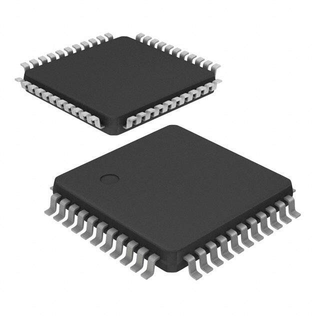
CY8C24094/CY8C24794 CY8C24894/CY8C24994 Pin Information This section describes, lists, and illustrates the CY8C24x94 PSoC device family pins and pinout configuration. The CY8C24x94 PSoC devices are available in the following packages, all of which are shown on the following pages. Every port pin (labeled with a “P”) is capable of Digital I/O. However, V , V , and XRES are not capable of Digital I/O. SS DD 56-Pin Part Pinout See LEGEND details and footnotes in Table 3 on page 10. Table 2. 56-Pin Part Pinout (QFN[6]) Pin Type Pin Type Name Description Name Description No. Digital Analog No. Digital Analog 1 I/O I, M P2[3] Direct switched capacitor block input Figure 4. CY8C24794 56-Pin PSoC Device [3] 2 I/O I, M P2[1] Direct switched capacitor block input M M 345 III///OOO MMM PPP444[[[753]]] P2[5], MP2[7], MP0[1], A, I, MP0[3], A, IO, P0[5], A, IO, P0[7], A, I, MVss VddP0[6], A, I, MP0[4], A, I, MP0[2], A, I, MP0[0], A, I, MP2[6], M P2[4], M 6 I/O M P4[1] 7 I/O M P3[7] A, I, M, P2[3] 1 5655545352 5150494847 4645 444342 P2[2], A, I, M 8 I/O M P3[5] A, I, M, P2[1] 2 41 P2[0], A, I, M 9 I/O M P3[3] M,P 4[7] 3 40 P4[6],M 10 I/O M P3[1] M,P 4[5] 4 39 P4[4],M 11 I/O M P5[7] M,P 4[3] 5 38 P4[2],M M,P 4[1] 6 37 P4[0],M 12 I/O M P5[5] M,P 3[7] 7 QFN 36 P3[6],M 13 I/O M P5[3] M,P 3[5] 8 (Top View) 35 P3[4],M 14 I/O M P5[1] M,P 3[3] 9 34 P3[2],M 15 I/O M P1[7] I2C serial clock (SCL) M,P 3[1] 10 33 P3[0],M M,P 5[7] 11 32 P5[6],M 16 I/O M P1[5] I2C serial data (SDA) M,P 5[5] 12 31 P5[4],M 17 I/O M P1[3] M,P 5[3] 13 30 P5[2],M 18 I/O M P1[1] I2C SCL, ISSP SCLK [4] M,P 5[1] 14151617181920 21222324 2526272829 P5[0],M 19 Power VSS Ground connection [5] 2222201234 II//OOPUUoSSwBBer PPVDD77D[[+–D70]] Supply voltage M, I2C SCL, P1[7]M, I2C SDA, P1[5] M, P1[3]M, I2C SCL, P1[1]VssD+D-VddP7[7] P7[0] M, I2C SDA, P1[0]M, P1[2]M, P1[4]EXTCLK,M, P1[6] 25 I/O M P1[0] I2C SDA, ISSP SDATA[4] 26 I/O M P1[2] 27 I/O M P1[4] Optional external clock input (EXTCLK) 28 I/O M P1[6] 29 I/O M P5[0] 30 I/O M P5[2] 31 I/O M P5[4] 44 I/O M P2[6] External voltage reference (VREF) input 32 I/O M P5[6] 45 I/O I, M P0[0] Analog column mux input 33 I/O M P3[0] 46 I/O I, M P0[2] Analog column mux input 34 I/O M P3[2] 47 I/O I, M P0[4] Analog column mux input VREF 35 I/O M P3[4] 48 I/O I, M P0[6] Analog column mux input 36 I/O M P3[6] 49 Power VDD Supply voltage 37 I/O M P4[0] 50 Power VSS Ground connection [5] 38 I/O M P4[2] 51 I/O I, M P0[7] Analog column mux input 39 I/O M P4[4] 52 I/O I/O, M P0[5] Analog column mux input and column output 40 I/O M P4[6] 53 I/O I/O, M P0[3] Analog column mux input and column output 41 I/O I, M P2[0] Direct switched capacitor block input 54 I/O I, M P0[1] Analog column mux input 42 I/O I, M P2[2] Direct switched capacitor block input 55 I/O M P2[7] 43 I/O M P2[4] External analog ground (AGND) input 56 I/O M P2[5] Notes 3. This part cannot be programmed with Reset mode; use Power Cycle mode when programming. 4. These are the ISSP pins, which are not High Z at POR. See the PSoC Technical Reference Manual for details. 5. All VSS pins should be brought out to one common GND plane. Document Number: 38-12018 Rev. AN Page 9 of 72
CY8C24094/CY8C24794 CY8C24894/CY8C24994 56-Pin Part Pinout (with XRES) Table 3. 56-Pin Part Pinout (QFN[6]) Pin Type Pin Type Name Description Name Description No. Digital Analog No. Digital Analog 1 I/O I, M P2[3] Direct switched capacitor block input Figure 5. CY8C24894 56-Pin PSoC Device 2 I/O I, M P2[1] Direct switched capacitor block input 3 I/O M P4[7] MM 45 II//OO MM PP44[[53]] MMA, I, MA, IO, A, IO, A, I, M A, I, MA, I, MA, I, MA, I, MMM 6 I/O M P4[1] P2[5], P2[7], P0[1], P0[3], P0[5], P0[7], VssVddP0[6], P0[4], P0[2], P0[0], P2[6], P2[4], 7 I/O M P3[7] 8 I/O M P3[5] A, I, M, P2[3] 1 565554535251504948474645444342 P2[2], A, I, M 9 I/O M P3[3] A, I, M, P2[1] 2 41 P2[0], A, I, M 10 I/O M P3[1] M, P4[7] 3 40 P4[6], M 11 I/O M P5[7] M, P4[5] 4 39 P4[4], M M, P4[3] 5 38 P4[2], M 12 I/O M P5[5] M, P4[1] 6 37 P4[0], M 13 I/O M P5[3] M, P3[7] 7 QFN 36 XRES 14 I/O M P5[1] M, P3[5] 8 (Top View) 35 P3[4], M 15 I/O M P1[7] I2C SCL M, P3[3] 9 34 P3[2], M 16 I/O M P1[5] I2C SDA MM,, PP35[[17]] 1101 3323 PP35[[06]],, MM 17 I/O M P1[3] M, P5[5] 12 31 P5[4], M 18 I/O M P1[1] I2C SCL, ISSP SCLK [7] M, P5[3] 13 30 P5[2], M 19 Power VSS Ground connection [8] M, P5[1] 14151617181920212223242526272829 P5[0], M 20 USB D+ 21 USB D– P1[7]P1[5]P1[3]P1[1]VssD+D-VddP7[7]P7[0]P1[0]P1[2]P1[4]P1[6] 2223 I/OPower PV7D[7D] Supply voltage SCL, SDA, M, SCL, SDA, M, K,M, M, 2245 II//OO M PP71[[00]] I2C SDA, ISSP SDATA[7] M, I2C M, I2C M, I2C M, I2C EXTCL 26 I/O M P1[2] 27 I/O M P1[4] Optional EXTCLK 28 I/O M P1[6] 29 I/O M P5[0] 30 I/O M P5[2] 31 I/O M P5[4] 44 I/O M P2[6] External VREF input 32 I/O M P5[6] 45 I/O I, M P0[0] Analog column mux input 33 I/O M P3[0] 46 I/O I, M P0[2] Analog column mux input 34 I/O M P3[2] 47 I/O I, M P0[4] Analog column mux input VREF 35 I/O M P3[4] 48 I/O I, M P0[6] Analog column mux input 36 Input XRES Active high external reset with internal 49 Power VDD Supply voltage pull-down 37 I/O M P4[0] 50 Power VSS Ground connection [8] 38 I/O M P4[2] 51 I/O I, M P0[7] Analog column mux input 39 I/O M P4[4] 52 I/O I/O, M P0[5] Analog column mux input and column output 40 I/O M P4[6] 53 I/O I/O, M P0[3] Analog column mux input and column output 41 I/O I, M P2[0] Direct switched capacitor block input 54 I/O I, M P0[1] Analog column mux input 42 I/O I, M P2[2] Direct switched capacitor block input 55 I/O M P2[7] 43 I/O M P2[4] External AGND input 56 I/O M P2[5] LEGEND A = Analog, I = Input, O = Output, and M = Analog Mux Input. Notes 6. The center pad on the QFN package should be connected to ground (VSS) for best mechanical, thermal, and electrical performance. If not connected to ground, it should be electrically floated and not connected to any other signal. 7. These are the ISSP pins, which are not High Z at POR. See the PSoC Technical Reference Manual for details. 8. All VSS pins should be brought out to one common GND plane. Document Number: 38-12018 Rev. AN Page 10 of 72
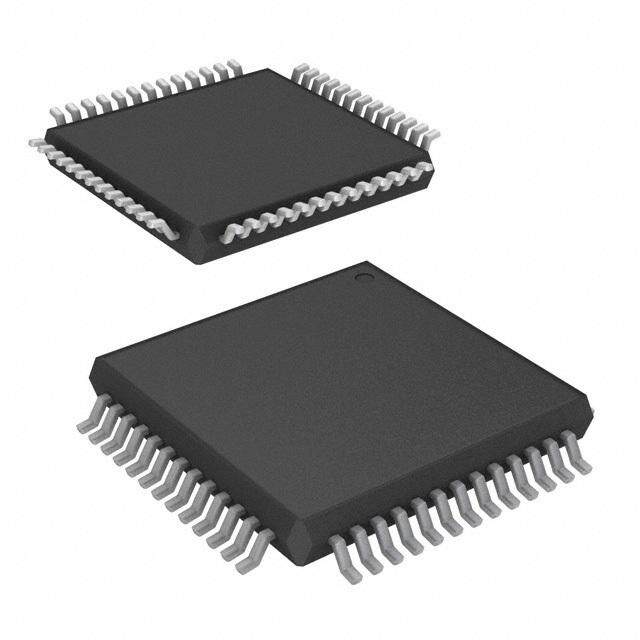
CY8C24094/CY8C24794 CY8C24894/CY8C24994 68-Pin Part Pinout The following 68-pin QFN part table and drawing is for the CY8C24994 PSoC device. Table 4. 68-Pin Part Pinout (QFN[9]) Pin Type Pin Type Name Description Name Description No. Digital Analog No. Digital Analog 1 I/O M P4[7] Figure 6. CY8C24994 68-Pin PSoC Device 2 I/O M P4[5] 3 I/O M P4[3] EFND RG 45 I/O M PN4C[1] No connection. Pin must be left floating AI AI AIAIOAIO AI AIAI AIAI Ext. VExt. AAI 67 Power VNSCS NGoro cuonndn ceocntinoenc. tPioinn m[10u]st be left floating P2[1], M, P2[3], M, P2[5], MP2[7], M P0[1], M, P0[3], M, P0[5], M, P0[7], M, VssVddP0[6], M, P0[4], M, P0[2], M, P0[0], M, P2[6], M, P2[4], M, P2[2], M, 8 I/O M P3[7] 87 65 4 32109 876 54 32 9 I/O M P3[5] 66 66 6 66665 555 55 55 M, P4[7] 1 51 P2[0], M, AI 10 I/O M P3[3] M, P4[5] 2 50 P4[6], M 11 I/O M P3[1] M, P4[3] 3 49 P4[4], M 12 I/O M P5[7] M, P4[1] 4 48 P4[2], M 13 I/O M P5[5] NC 5 47 P4[0], M NC 6 46 XRES 14 I/O M P5[3] Vss 7 45 NC 15 I/O M P5[1] M, P3[7] 8 QFN 44 NC 16 I/O M P1[7] I2C SCL M, P3[5] 9 43 P3[6], M 17 I/O M P1[5] I2C SDA M, P3[3] 10 (Top View) 42 P3[4], M M, P3[1] 11 41 P3[2], M 18 I/O M P1[3] M, P5[7] 12 40 P3[0], M 19 I/O M P1[1] I2C SCL ISSP SCLK[11] M, P5[5] 13 39 P5[6], M 2201 UPoSwBer VDS+S Ground connection [10] I2C SCL, MMM,,, PPP551[[[317]]] 111456 333876 PPP555[[[420]]],,, MMM 22 USB D– I2C SDA, M, P1[5] 17 35 P1[6], M 89 0123 4567 890 1234 23 Power VDD Supply voltage 11 2222 2222 223 3333 222456 III///OOO PPP777[[[765]]] M, P1[3] M, P1[1]VssD +D -Vdd P7[7]P7[6]P7[5]P7[4] P7[3]P7[2]P7[1]P7[0] M, P1[0]M, P1[2] M, P1[4] 2278 II//OO PP77[[43]] C SCL, C SDA, XTCLK, 29 I/O P7[2] I2 I2 E 30 I/O P7[1] 31 I/O P7[0] 50 I/O M P4[6] 32 I/O M P1[0] I2C SDA, ISSP SDATA[11] 51 I/O I, M P2[0] Direct switched capacitor block input 33 I/O M P1[2] 52 I/O I, M P2[2] Direct switched capacitor block input 34 I/O M P1[4] Optional EXTCLK 53 I/O M P2[4] External AGND input 35 I/O M P1[6] 54 I/O M P2[6] External VREF input 36 I/O M P5[0] 55 I/O I, M P0[0] Analog column mux input 37 I/O M P5[2] 56 I/O I, M P0[2] Analog column mux input and column output 38 I/O M P5[4] 57 I/O I, M P0[4] Analog column mux input and column output 39 I/O M P5[6] 58 I/O I, M P0[6] Analog column mux input 40 I/O M P3[0] 59 Power VDD Supply voltage 41 I/O M P3[2] 60 Power VSS Ground connection [10] 42 I/O M P3[4] 61 I/O I, M P0[7] Analog column mux input, integration input #1 43 I/O M P3[6] 62 I/O I/O, M P0[5] Analog column mux input and column output, integration input #2 44 NC No connection. Pin must be left floating. 63 I/O I/O, M P0[3] Analog column mux input and column output 45 NC No connection. Pin must be left floating. 64 I/O I, M P0[1] Analog column mux input 46 Input XRES Active high pin reset with internal 65 I/O M P2[7] pull-down. 47 I/O M P4[0] 66 I/O M P2[5] 48 I/O M P4[2] 67 I/O I, M P2[3] Direct switched capacitor block input 49 I/O M P4[4] 68 I/O I, M P2[1] Direct switched capacitor block input LEGEND A = Analog, I = Input, O = Output, NC = No connection. Pin must be left floating, M = Analog Mux Input. Notes 9. The center pad on the QFN package should be connected to ground (VSS) for best mechanical, thermal, and electrical performance. If not connected to ground, it should be electrically floated and not connected to any other signal. 10.All VSS pins should be brought out to one common GND plane. 11.These are the ISSP pins, which are not High Z at POR. See the PSoC Technical Reference Manual for details. Document Number: 38-12018 Rev. AN Page 11 of 72
CY8C24094/CY8C24794 CY8C24894/CY8C24994 68-Pin Part Pinout (On-Chip Debug) The following 68-pin QFN part table and drawing is for the CY8C24094 OCD PSoC device. Note: This part is only used for in-circuit debugging. It is NOT available for production. Table 5. 68-Pin Part Pinout (QFN[12]) Pin Type Pin Type Name Description Name Description No. Digital Analog No. Digital Analog 1 I/O M P4[7] Figure 7. CY8C24094 68-Pin OCD PSoC Device 2 I/O M P4[5] FD EN 3 I/O M P4[3] RG VA 4 I/O M P4[1] AI AI AIAIOAIO AI AIAIAIAI Ext. Ext. AI 5 OCDE OCD even data I/O M, M, MMM, M, M, M, M, M, M, M, M, M, M, 67 Power VOSCSDO OGCroDun odd dco dnanteac otiuotnp u[1t3] P2[1], P2[3], P2[5], P2[7], P0[1], P0[3], P0[5], P0[7], VssVddP0[6], P0[4], P0[2], P0[0], P2[6], P2[4], P2[2], 8 I/O M P3[7] 87 65 432109 876 5432 9 I/O M P3[5] M, P4[7] 166 66 666665 555 555551 P2[0], M, AI 10 I/O M P3[3] M, P4[5] 2 50 P4[6], M M, P4[3] 3 49 P4[4], M 11 I/O M P3[1] M, P4[1] 4 48 P4[2], M 12 I/O M P5[7] OCDE 5 47 P4[0], M 13 I/O M P5[5] OCDO 6 46 XRES 14 I/O M P5[3] Vss 7 45 CCLK M, P3[7] 8 44 HCLK 15 I/O M P5[1] M, P3[5] 9 QFN 43 P3[6], M 16 I/O M P1[7] I2C SCL M, P3[3] 10 (Top View) 42 P3[4], M 17 I/O M P1[5] I2C SDA M, P3[1] 11 41 P3[2], M M, P5[7] 12 40 P3[0], M 18 I/O M P1[3] M, P5[5] 13 39 P5[6], M 19 I/O M P1[1] I2C SCL, ISSP SCLK [14] M, P5[3] 14 38 P5[4], M 20 Power VSS Ground connection [13] M, P5[1] 15 37 P5[2], M 21 USB D+ I2C SCL, M, P1[7] 16 36 P5[0], M I2C SDA, M, P1[5] 17 35 P1[6], M 22 USB D– 89 012 34567 8901234 11 222 22222 2233333 23 Power VDD Supply voltage 24 I/O P7[7] P1[3]P1[1]VssD +D -Vdd P7[7]P7[6]P7[5]P7[4] P7[3]P7[2]P7[1]P7[0] P1[0]P1[2]P1[4] 25 I/O P7[6] M, M, M, M, M, 222678 III///OOO PPP777[[[543]]] I2C SCL, I2C SDA, EXTCLK, 29 I/O P7[2] 30 I/O P7[1] 31 I/O P7[0] 50 I/O M P4[6] 32 I/O M P1[0] I2C SDA, ISSP SDATA[14] 51 I/O I, M P2[0] Direct switched capacitor block input 33 I/O M P1[2] 52 I/O I, M P2[2] Direct switched capacitor block input 34 I/O M P1[4] Optional EXTCLK 53 I/O M P2[4] External AGND input 35 I/O M P1[6] 54 I/O M P2[6] External VREF input 36 I/O M P5[0] 55 I/O I, M P0[0] Analog column mux input 37 I/O M P5[2] 56 I/O I, M P0[2] Analog column mux input and column output 38 I/O M P5[4] 57 I/O I, M P0[4] Analog column mux input and column output 39 I/O M P5[6] 58 I/O I, M P0[6] Analog column mux input 40 I/O M P3[0] 59 Power VDD Supply voltage 41 I/O M P3[2] 60 Power VSS Ground connection [13] 42 I/O M P3[4] 61 I/O I, M P0[7] Analog column mux input, integration input #1 43 I/O M P3[6] 62 I/O I/O, M P0[5] Analog column mux input and column output, integration input #2 44 HCLK OCD high speed clock output 63 I/O I/O, M P0[3] Analog column mux input and column output 45 CCLK OCD CPU clock output 64 I/O I, M P0[1] Analog column mux input 46 Input XRES Active high pin reset with internal pull-down 65 I/O M P2[7] 47 I/O M P4[0] 66 I/O M P2[5] 48 I/O M P4[2] 67 I/O I, M P2[3] Direct switched capacitor block input 49 I/O M P4[4] 68 I/O I, M P2[1] Direct switched capacitor block input LEGEND A = Analog, I = Input, O = Output, M = Analog Mux Input, OCD = On-Chip Debugger. Notes 12.The center pad on the QFN package should be connected to ground (VSS) for best mechanical, thermal, and electrical performance. If not connected to ground, it should be electrically floated and not connected to any other signal. 13.All VSS pins should be brought out to one common GND plane. 14.These are the ISSP pins, which are not High Z at POR. See the PSoC Technical Reference Manual for details. Document Number: 38-12018 Rev. AN Page 12 of 72
CY8C24094/CY8C24794 CY8C24894/CY8C24994 100-Ball VFBGA Part Pinout The 100-ball VFBGA part is for the CY8C24994 PSoC device. Table 6. 100-Ball Part Pinout (VFBGA[15]) NPion. Digital Analog Name Description NPion. Digital Analog Name Description A1 Power VSS Ground connection F1 NC No connection. Pin must be left floating A2 Power VSS Ground connection F2 I/O M P5[7] A3 NC No connection. Pin must be left floating F3 I/O M P3[5] A4 NC No connection. Pin must be left floating F4 I/O M P5[1] A5 NC No connection. Pin must be left floating F5 Power VSS Ground connection A6 Power VDD Supply voltage F6 Power VSS Ground connection A7 NC No connection. Pin must be left floating F7 I/O M P5[0] A8 NC No connection. Pin must be left floating F8 I/O M P3[0] A9 Power VSS Ground connection F9 XRES Active high pin reset with internal pull-down A10 Power VSS Ground connection F10 I/O P7[1] B1 Power VSS Ground connection G1 NC No connection. Pin must be left floating B2 Power VSS Ground connection G2 I/O M P5[5] B3 I/O I, M P2[1] Direct switched capacitor block input G3 I/O M P3[3] B4 I/O I, M P0[1] Analog column mux input G4 I/O M P1[7] I2C SCL B5 I/O I, M P0[7] Analog column mux input G5 I/O M P1[1] I2C SCL, ISSP SCLK[16] B6 Power VDD Supply voltage G6 I/O M P1[0] I2C SDA, ISSP SDATA[16] B7 I/O I, M P0[2] Analog column mux input G7 I/O M P1[6] B8 I/O I, M P2[2] Direct switched capacitor block input G8 I/O M P3[4] B9 Power VSS Ground connection G9 I/O M P5[6] B10 Power VSS Ground connection G10 I/O P7[2] C1 NC No connection. Pin must be left floating H1 NC No connection. Pin must be left floating C2 I/O M P4[1] H2 I/O M P5[3] C3 I/O M P4[7] H3 I/O M P3[1] C4 I/O M P2[7] H4 I/O M P1[5] I2C SDA C5 I/O I/O, M P0[5] Analog column mux input and column output H5 I/O M P1[3] C6 I/O I, M P0[6] Analog column mux input H6 I/O M P1[2] C7 I/O I, M P0[0] Analog column mux input H7 I/O M P1[4] Optional EXTCLK C8 I/O I, M P2[0] Direct switched capacitor block input H8 I/O M P3[2] C9 I/O M P4[2] H9 I/O M P5[4] C10 NC No connection. Pin must be left floating H10 I/O P7[3] D1 NC No connection. Pin must be left floating J1 Power VSS Ground connection D2 I/O M P3[7] J2 Power VSS Ground connection D3 I/O M P4[5] J3 USB D+ D4 I/O M P2[5] J4 USB D– D5 I/O I/O, M P0[3] Analog column mux input and column output J5 Power VDD Supply voltage D6 I/O I,M P0[4] Analog column mux input J6 I/O P7[7] D7 I/O M P2[6] External VREF input J7 I/O P7[0] D8 I/O M P4[6] J8 I/O M P5[2] D9 I/O M P4[0] J9 Power VSS Ground connection D10 NC No connection. Pin must be left floating J10 Power VSS Ground connection E1 NC No connection. Pin must be left floating K1 Power VSS Ground connection E2 NC No connection. Pin must be left floating K2 Power VSS Ground connection E3 I/O M P4[3] K3 NC No connection. Pin must be left floating E4 I/O I, M P2[3] Direct switched capacitor block input K4 NC No connection. Pin must be left floating E5 Power VSS Ground connection K5 Power VDD Supply voltage E6 Power VSS Ground connection K6 I/O P7[6] E7 I/O M P2[4] External AGND input K7 I/O P7[5] E8 I/O M P4[4] K8 I/O P7[4] E9 I/O M P3[6] K9 Power VSS Ground connection E10 NC No connection. Pin must be left floating K10 Power VSS Ground connection LEGEND A = Analog, I = Input, O = Output, M = Analog Mux Input, NC = No connection. Pin must be left floating. Notes 15.All VSS pins should be brought out to one common GND plane. 16.These are the ISSP pins, which are not High Z at POR. See the PSoC Technical Reference Manual for details. Document Number: 38-12018 Rev. AN Page 13 of 72
CY8C24094/CY8C24794 CY8C24894/CY8C24994 Figure 8. CY8C24094 OCD (Not for Production) 1 2 3 4 5 6 7 8 9 10 A Vss Vss NC NC NC Vdd NC NC Vss Vss B Vss Vss P2[1] P0[1] P0[7] Vdd P0[2] P2[2] Vss Vss C NC P4[1] P4[7] P2[7] P0[5] P0[6] P0[0] P2[0] P4[2] NC D NC P3[7] P4[5] P2[5] P0[3] P0[4] P2[6] P4[6] P4[0] NC E NC NC P4[3] P2[3] Vss Vss P2[4] P4[4] P3[6] NC F NC P5[7] P3[5] P5[1] Vss Vss P5[0] P3[0] XRES P7[1] G NC P5[5] P3[3] P1[7] P1[1] P1[0] P1[6] P3[4] P5[6] P7[2] H NC P5[3] P3[1] P1[5] P1[3] P1[2] P1[4] P3[2] P5[4] P7[3] J Vss Vss D + D - Vdd P7[7] P7[0] P5[2] Vss Vss K Vss Vss NC NC Vdd P7[6] P7[5] P7[4] Vss Vss BGA (Top View) Document Number: 38-12018 Rev. AN Page 14 of 72
CY8C24094/CY8C24794 CY8C24894/CY8C24994 100-Ball VFBGA Part Pinout (On-Chip Debug) The following 100-pin VFBGA part table and drawing is for the CY8C24094 OCD PSoC device. Note This part is only used for in-circuit debugging. It is NOT available for production. Table 7. 100-Ball Part Pinout (VFBGA[17]) NPion. Digital Analog Name Description NPion. Digital Analog Name Description A1 Power VSS Ground connection F1 OCDE OCD even data I/O A2 Power VSS Ground connection F2 I/O M P5[7] A3 NC No connection. Pin must be left floating F3 I/O M P3[5] A4 NC No connection. Pin must be left floating F4 I/O M P5[1] A5 NC No connection. Pin must be left floating. F5 Power VSS Ground connection A6 Power VDD Supply voltage. F6 Power VSS Ground connection A7 NC No connection. Pin must be left floating. F7 I/O M P5[0] A8 NC No connection. Pin must be left floating. F8 I/O M P3[0] A9 Power VSS Ground connection F9 XRES Active high pin reset with internal pull-down A10 Power VSS Ground connection F10 I/O P7[1] B1 Power VSS Ground connection G1 OCDO OCD odd data output B2 Power VSS Ground connection G2 I/O M P5[5] B3 I/O I, M P2[1] Direct switched capacitor block input G3 I/O M P3[3] B4 I/O I, M P0[1] Analog column mux input G4 I/O M P1[7] I2C SCL B5 I/O I, M P0[7] Analog column mux input G5 I/O M P1[1] I2C SCL, ISSP SCLK[18] B6 Power VDD Supply voltage G6 I/O M P1[0] I2C SDA, ISSP SDATA[18] B7 I/O I, M P0[2] Analog column mux input G7 I/O M P1[6] B8 I/O I, M P2[2] Direct switched capacitor block input G8 I/O M P3[4] B9 Power VSS Ground connection G9 I/O M P5[6] B10 Power VSS Ground connection G10 I/O P7[2] C1 NC No connection. Pin must be left floating H1 NC No connection. Pin must be left floating C2 I/O M P4[1] H2 I/O M P5[3] C3 I/O M P4[7] H3 I/O M P3[1] C4 I/O M P2[7] H4 I/O M P1[5] I2C SDA C5 I/O I/O,M P0[5] Analog column mux input and column output H5 I/O M P1[3] C6 I/O I, M P0[6] Analog column mux input H6 I/O M P1[2] C7 I/O I, M P0[0] Analog column mux input H7 I/O M P1[4] Optional EXTCLK C8 I/O I, M P2[0] Direct switched capacitor block input H8 I/O M P3[2] C9 I/O M P4[2] H9 I/O M P5[4] C10 NC No connection. Pin must be left floating H10 I/O P7[3] D1 NC No connection. Pin must be left floating J1 Power VSS Ground connection D2 I/O M P3[7] J2 Power VSS Ground connection D3 I/O M P4[5] J3 USB D+ D4 I/O M P2[5] J4 USB D- D5 I/O I/O, M P0[3] Analog column mux input and column output J5 Power VDD Supply voltage D6 I/O I, M P0[4] Analog column mux input J6 I/O P7[7] D7 I/O M P2[6] External VREF input J7 I/O P7[0] D8 I/O M P4[6] J8 I/O M P5[2] D9 I/O M P4[0] J9 Power VSS Ground connection D10 CCLK OCD CPU clock output J10 Power VSS Ground connection E1 NC No connection. Pin must be left floating K1 Power VSS Ground connection E2 NC No connection. Pin must be left floating K2 Power VSS Ground connection E3 I/O M P4[3] K3 NC No connection. Pin must be left floating E4 I/O I, M P2[3] Direct switched capacitor block input K4 NC No connection. Pin must be left floating E5 Power VSS Ground connection K5 Power VDD Supply voltage E6 Power VSS Ground connection K6 I/O P7[6] E7 I/O M P2[4] External AGND input K7 I/O P7[5] E8 I/O M P4[4] K8 I/O P7[4] E9 I/O M P3[6] K9 Power VSS Ground connection E10 HCLK OCD high speed clock output K10 Power VSS Ground connection LEGEND A = Analog, I = Input, O = Output, M = Analog Mux Input, NC = No connection. Pin must be left floating, OCD = On-Chip Debugger. Notes 17.All VSS pins should be brought out to one common GND plane. 18.These are the ISSP pins, which are not High Z at POR. See the PSoC Technical Reference Manual for details. Document Number: 38-12018 Rev. AN Page 15 of 72
CY8C24094/CY8C24794 CY8C24894/CY8C24994 Figure 9. CY8C24094 OCD (Not for Production) 1 2 3 4 5 6 7 8 9 10 A Vss Vss NC NC NC Vdd NC NC Vss Vss B Vss Vss P2[1] P0[1] P0[7] Vdd P0[2] P2[2] Vss Vss C NC P4[1] P4[7] P2[7] P0[5] P0[6] P0[0] P2[0] P4[2] NC D NC P3[7] P4[5] P2[5] P0[3] P0[4] P2[6] P4[6] P4[0] CClk E NC NC P4[3] P2[3] Vss Vss P2[4] P4[4] P3[6] HClk F ocde P5[7] P3[5] P5[1] Vss Vss P5[0] P3[0] XRES P7[1] G ocdo P5[5] P3[3] P1[7] P1[1] P1[0] P1[6] P3[4] P5[6] P7[2] H NC P5[3] P3[1] P1[5] P1[3] P1[2] P1[4] P3[2] P5[4] P7[3] J Vss Vss D + D - Vdd P7[7] P7[0] P5[2] Vss Vss K Vss Vss NC NC Vdd P7[6] P7[5] P7[4] Vss Vss BGA (Top View) Document Number: 38-12018 Rev. AN Page 16 of 72
CY8C24094/CY8C24794 CY8C24894/CY8C24994 100-Pin Part Pinout (On-Chip Debug) The 100-pin TQFP part is for the CY8C24094 OCD PSoC device. Note: This part is only used for in-circuit debugging. It is NOT available for production. Table 8. 100-Pin Part Pinout (TQFP[19]) NPion. Digital Analog Name Description NPion. Digital Analog Name Description 1 NC No connection. Pin must be left floating 51 I/O M P1[6] 2 NC No connection. Pin must be left floating 52 I/O M P5[0] 3 I/O I, M P0[1] Analog column mux input 53 I/O M P5[2] 4 I/O M P2[7] 54 I/O M P5[4] 5 I/O M P2[5] 55 I/O M P5[6] 6 I/O I, M P2[3] Direct switched capacitor block input 56 I/O M P3[0] 7 I/O I, M P2[1] Direct switched capacitor block input 57 I/O M P3[2] 8 I/O M P4[7] 58 I/O M P3[4] 9 I/O M P4[5] 59 I/O M P3[6] 10 I/O M P4[3] 60 HCLK OCD high speed clock output 11 I/O M P4[1] 61 CCLK OCD CPU clock output 12 OCDE OCD even data I/O 62 Input XRES Active high pin reset with internal pull-down 13 OCDO OCD odd data output 63 I/O M P4[0] 14 NC No connection. Pin must be left floating 64 I/O M P4[2] 15 Power VSS Ground connection 65 Power VSS Ground connection 16 I/O M P3[7] 66 I/O M P4[4] 17 I/O M P3[5] 67 I/O M P4[6] 18 I/O M P3[3] 68 I/O I, M P2[0] Direct switched capacitor block input 19 I/O M P3[1] 69 I/O I, M P2[2] Direct switched capacitor block input 20 I/O M P5[7] 70 I/O P2[4] External AGND input 21 I/O M P5[5] 71 NC No connection. Pin must be left floating 22 I/O M P5[3] 72 I/O P2[6] External VREF input 23 I/O M P5[1] 73 NC No connection. Pin must be left floating 24 I/O M P1[7] I2C SCL 74 I/O I P0[0] Analog column mux input 25 NC No connection. Pin must be left floating 75 NC No connection. Pin must be left floating 26 NC No connection. Pin must be left floating 76 NC No connection. Pin must be left floating 27 NC No connection. Pin must be left floating 77 I/O I, M P0[2] Analog column mux input and column output 28 I/O P1[5] I2C SDA 78 NC No connection. Pin must be left floating 29 I/O P1[3] 79 I/O I, M P0[4] Analog column mux input and column output 30 I/O P1[1] Crystal (XTALin), I2C SCL, ISSP SCLK[20] 80 NC No connection. Pin must be left floating 31 NC No connection. Pin must be left floating 81 I/O I, M P0[6] Analog column mux input 32 Power VSS Ground connection 82 Power VDD Supply voltage 33 USB D+ 83 NC No connection. Pin must be left floating 34 USB D- 84 Power VSS Ground connection 35 Power VDD Supply voltage 85 NC No connection. Pin must be left floating 36 I/O P7[7] 86 NC No connection. Pin must be left floating 37 I/O P7[6] 87 NC No connection. Pin must be left floating 38 I/O P7[5] 88 NC No connection. Pin must be left floating 39 I/O P7[4] 89 NC No connection. Pin must be left floating 40 I/O P7[3] 90 NC No connection. Pin must be left floating 41 I/O P7[2] 91 NC No connection. Pin must be left floating 42 I/O P7[1] 92 NC No connection. Pin must be left floating 43 I/O P7[0] 93 NC No connection. Pin must be left floating 44 NC No connection. Pin must be left floating 94 NC No connection. Pin must be left floating 45 NC No connection. Pin must be left floating 95 I/O I, M P0[7] Analog column mux input 46 NC No connection. Pin must be left floating 96 NC No connection. Pin must be left floating 47 NC No connection. Pin must be left floating 97 I/O I/O, M P0[5] Analog column mux input and column output 48 I/O P1[0] Crystal (XTALout), I2C SDA, ISSP SDATA[20] 98 NC No connection. Pin must be left floating 49 I/O P1[2] 99 I/O I/O, M P0[3] Analog column mux input and column output 50 I/O P1[4] Optional EXTCLK 100 NC No connection. Pin must be left floating LEGEND A = Analog, I = Input, O = Output, NC = No connection. Pin must be left floating, M = Analog Mux Input, OCD = On-Chip Debugger. Notes 19.All VSS pins should be brought out to one common GND plane. 20.These are the ISSP pins, which are not High Z at POR. See the PSoC Technical Reference Manual for details. Document Number: 38-12018 Rev. AN Page 17 of 72
CY8C24094/CY8C24794 CY8C24894/CY8C24994 Figure 10. CY8C24094 OCD (Not for Production) AI AI AI AI AI AI M, M, M, M, M, M, 3], 5], 7], 6], 4], 2], C 0[ C0[ C 0[C CCC C C C C CCss Cdd 0[C0[ C 0[ C N P NP N PN NNN N N N N NNV NV PNP N P N NC 1 10099 9897 96 95 9493 9291 9089 88 87 86 85 8483 8281 80 79 78 777675 NC NC 2 74 P0[0], M, AI AI, M, P0[1] 3 73 NC M,P 2[7] 4 72 P2[6], M,E xternal VREF M,P 2[5] 5 71 NC AI, M, P2[3] 6 70 P2[4], M,E xternal AGND AI, M, P2[1] 7 69 P2[2], M, AI M,P 4[7] 8 68 P2[0], M, AI M,P 4[5] 9 67 P4[6],M M,P 4[3] 10 66 P4[4],M M,P 4[1] 11 65 Vss OCDE 12 64 P4[2],M OCDO 13 TQFP 63 P4[0],M NC 14 62 XRES Vss 15 61 CCLK M,P 3[7] 16 60 HCLK M,P 3[5] 17 59 P3[6],M M,P 3[3] 18 58 P3[4],M M,P 3[1] 19 57 P3[2],M M,P 5[7] 20 56 P3[0],M M,P 5[5] 21 55 P5[6],M M,P 5[3] 22 54 P5[4],M M,P 5[1] 23 53 P5[2],M I2C SCL, P1[7] 24 52 P5[0],M NC 25 51 P1[6],M 67 89 0 1 234 5 67 8 90 1 2 3 45 6 7 8 90 22 22 3 3 333 3 33 3 34 4 4 4 44 4 4 4 45 NC NC M, P1[5]M, P1[3] M, P1[1]NC Vss D+D- Vdd P7[7]P7[6]P7[5] P7[4] P7[3]P7[2] P7[1] P7[0] NCNCNCNC M, P1[0] M, P1[2]M, P1[4] A, L, A, K, D C D L S S S C I2C I2C I2C EXT Document Number: 38-12018 Rev. AN Page 18 of 72
CY8C24094/CY8C24794 CY8C24894/CY8C24994 Register Reference This section lists the registers of the CY8C24x94 PSoC device family. For detailed register information, see the PSoC Technical Reference Manual. Register Conventions Register Mapping Tables The register conventions specific to this section are listed in the The PSoC device has a total register address space of following table. 512bytes. The register space is referred to as I/O space and is divided into two banks, Bank 0 and Bank 1. The XOI bit in the Convention Description Flag register (CPU_F) determines which bank the user is currently in. When the XOI bit is set to 1, the user is in Bank 1. R Read register or bit(s) Note: In the following register mapping tables, blank fields are W Write register or bit(s) Reserved and should not be accessed. L Logical register or bit(s) C Clearable register or bit(s) # Access is bit specific Document Number: 38-12018 Rev. AN Page 19 of 72
CY8C24094/CY8C24794 CY8C24894/CY8C24994 Register Map Bank 0 Table: User Space Name Addr (0, Hex) Access Name Addr (0, Hex) Access Name Addr (0, Hex) Access Name Addr (0, Hex) Access PRT0DR 00 RW PMA0_DR 40 RW ASC10CR0 80 RW C0 PRT0IE 01 RW PMA1_DR 41 RW ASC10CR1 81 RW C1 PRT0GS 02 RW PMA2_DR 42 RW ASC10CR2 82 RW C2 PRT0DM2 03 RW PMA3_DR 43 RW ASC10CR3 83 RW C3 PRT1DR 04 RW PMA4_DR 44 RW ASD11CR0 84 RW C4 PRT1IE 05 RW PMA5_DR 45 RW ASD11CR1 85 RW C5 PRT1GS 06 RW PMA6_DR 46 RW ASD11CR2 86 RW C6 PRT1DM2 07 RW PMA7_DR 47 RW ASD11CR3 87 RW C7 PRT2DR 08 RW USB_SOF0 48 R 88 C8 PRT2IE 09 RW USB_SOF1 49 R 89 C9 PRT2GS 0A RW USB_CR0 4A RW 8A CA PRT2DM2 0B RW USBI/O_CR0 4B # 8B CB PRT3DR 0C RW USBI/O_CR1 4C RW 8C CC PRT3IE 0D RW 4D 8D CD PRT3GS 0E RW EP1_CNT1 4E # 8E CE PRT3DM2 0F RW EP1_CNT 4F RW 8F CF PRT4DR 10 RW EP2_CNT1 50 # ASD20CR0 90 RW CUR_PP D0 RW PRT4IE 11 RW EP2_CNT 51 RW ASD20CR1 91 RW STK_PP D1 RW PRT4GS 12 RW EP3_CNT1 52 # ASD20CR2 92 RW D2 PRT4DM2 13 RW EP3_CNT 53 RW ASD20CR3 93 RW IDX_PP D3 RW PRT5DR 14 RW EP4_CNT1 54 # ASC21CR0 94 RW MVR_PP D4 RW PRT5IE 15 RW EP4_CNT 55 RW ASC21CR1 95 RW MVW_PP D5 RW PRT5GS 16 RW EP0_CR 56 # ASC21CR2 96 RW I2C_CFG D6 RW PRT5DM2 17 RW EP0_CNT 57 # ASC21CR3 97 RW I2C_SCR D7 # 18 EP0_DR0 58 RW 98 I2C_DR D8 RW 19 EP0_DR1 59 RW 99 I2C_MSCR D9 # 1A EP0_DR2 5A RW 9A INT_CLR0 DA RW 1B EP0_DR3 5B RW 9B INT_CLR1 DB RW PRT7DR 1C RW EP0_DR4 5C RW 9C INT_CLR2 DC RW PRT7IE 1D RW EP0_DR5 5D RW 9D INT_CLR3 DD RW PRT7GS 1E RW EP0_DR6 5E RW 9E INT_MSK3 DE RW PRT7DM2 1F RW EP0_DR7 5F RW 9F INT_MSK2 DF RW DBB00DR0 20 # AMX_IN 60 RW A0 INT_MSK0 E0 RW DBB00DR1 21 W AMUXCFG 61 RW A1 INT_MSK1 E1 RW DBB00DR2 22 RW 62 A2 INT_VC E2 RC DBB00CR0 23 # ARF_CR 63 RW A3 RES_WDT E3 W DBB01DR0 24 # CMP_CR0 64 # A4 DEC_DH E4 RC DBB01DR1 25 W ASY_CR 65 # A5 DEC_DL E5 RC DBB01DR2 26 RW CMP_CR1 66 RW A6 DEC_CR0 E6 RW DBB01CR0 27 # 67 A7 DEC_CR1 E7 RW DCB02DR0 28 # 68 MUL1_X A8 W MUL0_X E8 W DCB02DR1 29 W 69 MUL1_Y A9 W MUL0_Y E9 W DCB02DR2 2A RW 6A MUL1_DH AA R MUL0_DH EA R DCB02CR0 2B # 6B MUL1_DL AB R MUL0_DL EB R DCB03DR0 2C # TMP_DR0 6C RW ACC1_DR1 AC RW ACC0_DR1 EC RW DCB03DR1 2D W TMP_DR1 6D RW ACC1_DR0 AD RW ACC0_DR0 ED RW DCB03DR2 2E RW TMP_DR2 6E RW ACC1_DR3 AE RW ACC0_DR3 EE RW DCB03CR0 2F # TMP_DR3 6F RW ACC1_DR2 AF RW ACC0_DR2 EF RW 30 ACB00CR3 70 RW RDI0RI B0 RW F0 31 ACB00CR0 71 RW RDI0SYN B1 RW F1 32 ACB00CR1 72 RW RDI0IS B2 RW F2 33 ACB00CR2 73 RW RDI0LT0 B3 RW F3 34 ACB01CR3 74 RW RDI0LT1 B4 RW F4 35 ACB01CR0 75 RW RDI0RO0 B5 RW F5 36 ACB01CR1 76 RW RDI0RO1 B6 RW F6 37 ACB01CR2 77 RW B7 CPU_F F7 RL 38 78 B8 F8 39 79 B9 F9 3A 7A BA FA 3B 7B BB FB 3C 7C BC FC 3D 7D BD DAC_D FD RW 3E 7E BE CPU_SCR1 FE # 3F 7F BF CPU_SCR0 FF # Blank fields are reserved and should not be accessed. # Access is bit specific. Document Number: 38-12018 Rev. AN Page 20 of 72
CY8C24094/CY8C24794 CY8C24894/CY8C24994 Register Map Bank 1 Table: Configuration Space Name Addr (1, Hex) Access Name Addr (1, Hex) Access Name Addr (1, Hex) Access Name Addr (1, Hex) Access PRT0DM0 00 RW PMA0_WA 40 RW ASC10CR0 80 RW USBI/O_CR2 C0 RW PRT0DM1 01 RW PMA1_WA 41 RW ASC10CR1 81 RW USB_CR1 C1 # PRT0IC0 02 RW PMA2_WA 42 RW ASC10CR2 82 RW PRT0IC1 03 RW PMA3_WA 43 RW ASC10CR3 83 RW PRT1DM0 04 RW PMA4_WA 44 RW ASD11CR0 84 RW EP1_CR0 C4 # PRT1DM1 05 RW PMA5_WA 45 RW ASD11CR1 85 RW EP2_CR0 C5 # PRT1IC0 06 RW PMA6_WA 46 RW ASD11CR2 86 RW EP3_CR0 C6 # PRT1IC1 07 RW PMA7_WA 47 RW ASD11CR3 87 RW EP4_CR0 C7 # PRT2DM0 08 RW 48 88 C8 PRT2DM1 09 RW 49 89 C9 PRT2IC0 0A RW 4A 8A CA PRT2IC1 0B RW 4B 8B CB PRT3DM0 0C RW 4C 8C CC PRT3DM1 0D RW 4D 8D CD PRT3IC0 0E RW 4E 8E CE PRT3IC1 0F RW 4F 8F CF PRT4DM0 10 RW PMA0_RA 50 RW 90 GDI_O_IN D0 RW PRT4DM1 11 RW PMA1_RA 51 RW ASD20CR1 91 RW GDI_E_IN D1 RW PRT4IC0 12 RW PMA2_RA 52 RW ASD20CR2 92 RW GDI_O_OU D2 RW PRT4IC1 13 RW PMA3_RA 53 RW ASD20CR3 93 RW GDI_E_OU D3 RW PRT5DM0 14 RW PMA4_RA 54 RW ASC21CR0 94 RW D4 PRT5DM1 15 RW PMA5_RA 55 RW ASC21CR1 95 RW D5 PRT5IC0 16 RW PMA6_RA 56 RW ASC21CR2 96 RW D6 PRT5IC1 17 RW PMA7_RA 57 RW ASC21CR3 97 RW D7 18 58 98 MUX_CR0 D8 RW 19 59 99 MUX_CR1 D9 RW 1A 5A 9A MUX_CR2 DA RW 1B 5B 9B MUX_CR3 DB RW PRT7DM0 1C RW 5C 9C DC PRT7DM1 1D RW 5D 9D OSC_GO_EN DD RW PRT7IC0 1E RW 5E 9E OSC_CR4 DE RW PRT7IC1 1F RW 5F 9F OSC_CR3 DF RW DBB00FN 20 RW CLK_CR0 60 RW A0 OSC_CR0 E0 RW DBB00IN 21 RW CLK_CR1 61 RW A1 OSC_CR1 E1 RW DBB00OU 22 RW ABF_CR0 62 RW A2 OSC_CR2 E2 RW 23 AMD_CR0 63 RW A3 VLT_CR E3 RW DBB01FN 24 RW CMP_GO_EN 64 RW A4 VLT_CMP E4 R DBB01IN 25 RW 65 A5 E5 DBB01OU 26 RW AMD_CR1 66 RW A6 E6 27 ALT_CR0 67 RW A7 E7 DCB02FN 28 RW 68 A8 IMO_TR E8 W DCB02IN 29 RW 69 A9 ILO_TR E9 W DCB02OU 2A RW 6A AA BDG_TR EA RW 2B 6B AB ECO_TR EB W DCB03FN 2C RW TMP_DR0 6C RW AC MUX_CR4 EC RW DCB03IN 2D RW TMP_DR1 6D RW AD MUX_CR5 ED RW DCB03OU 2E RW TMP_DR2 6E RW AE EE 2F TMP_DR3 6F RW AF EF 30 ACB00CR3 70 RW RDI0RI B0 RW F0 31 ACB00CR0 71 RW RDI0SYN B1 RW F1 32 ACB00CR1 72 RW RDI0IS B2 RW F2 33 ACB00CR2 73 RW RDI0LT0 B3 RW F3 34 ACB01CR3 74 RW RDI0LT1 B4 RW F4 35 ACB01CR0 75 RW RDI0RO0 B5 RW F5 36 ACB01CR1 76 RW RDI0RO1 B6 RW F6 37 ACB01CR2 77 RW B7 CPU_F F7 RL 38 78 B8 F8 39 79 B9 F9 3A 7A BA FA 3B 7B BB FB 3C 7C BC FC 3D 7D BD DAC_CR FD RW 3E 7E BE CPU_SCR1 FE # 3F 7F BF CPU_SCR0 FF # Blank fields are reserved and should not be accessed. # Access is bit specific. Document Number: 38-12018 Rev. AN Page 21 of 72
CY8C24094/CY8C24794 CY8C24894/CY8C24994 Electrical Specifications This section presents the DC and AC electrical specifications of the CY8C24x94 PSoC device family. For the most up-to-date electrical specifications, confirm that you have the most recent datasheet by visiting http://www.cypress.com. Specifications are valid for –40 °C T 85 °C and T 100 °C, except where noted. Specifications for devices when used in USB A J applications with IMO > 12 MHz and VDD = 3.3 V are valid for –40 °C <= TA <= 70 °C and TJ <= 82 °C. Figure 11. Voltage Versus CPU Frequency 5.25 4.75 O V peali oltage Regiornatingd V d d V 3.00 93 kHz 12 MHz 24 MHz CPU Frequency Absolute Maximum Ratings Table 9. Absolute Maximum Ratings Parameter Description Min Typ Max Units Notes T Storage temperature –55 25 +100 °C Higher storage temperatures STG reduces data retention time. Recommended storage temperature is +25 °C ± 25 °C. Extended duration storage temperatures higher than 65°C degrades reliability. T Bake temperature – 125 See °C BAKETEMP package label t Bake time See – 72 Hours BAKETIME package label T Ambient temperature with power applied –40 – +85 °C A V Supply voltage on V relative to V –0.5 – +6.0 V DD DD SS V DC input voltage V – 0.5 – V + 0.5 V I/O SS DD V DC voltage applied to tristate V – 0.5 – V + 0.5 V I/O2 SS DD I Maximum current into any port pin –25 – +50 mA MI/O I Maximum current into any port pin configured –50 – +50 mA MAI/O as analog driver ESD Electrostatic discharge voltage 2000 – – V Human body model ESD. LU Latch-up current – – 200 mA Document Number: 38-12018 Rev. AN Page 22 of 72
CY8C24094/CY8C24794 CY8C24894/CY8C24994 Operating Temperature Table 10. Operating Temperature Parameter Description Min Typ Max Units Notes T Ambient temperature –40 – +85 °C A T Ambient temperature using USB –10 – +85 °C AUSB T Junction temperature –40 – +100 °C The temperature rise from J ambient to junction is package specific. See Thermal Impedance on page 49. The user must limit the power consumption to comply with this requirement. DC Electrical Characteristics DC Chip-Level Specifications The following table lists guaranteed maximum and minimum specifications for the voltage and temperature ranges: 4.75 V to 5.25 V and –40 °C T 85 °C, or 3.0 V to 3.6 V and –40 °C T 85 °C, respectively. Typical parameters are measured at 5 V and 3.3 V A A at 25 °C and are for design guidance only. Table 11. DC Chip-Level Specifications Parameter Description Min Typ Max Units Notes V Supply voltage 3.0 – 5.25 V See DC POR and LVD specifications, DD Table 22 on page 38. I Supply current, IMO = 24 MHz (5 V) – 14 27 mA Conditions are V = 5.0 V, T = 25 °C, DD5 DD A CPU = 3 MHz, SYSCLK doubler disabled, VC1 = 1.5 MHz, VC2 = 93.75 kHz, VC3 = 93.75 kHz, analog power = off. I Supply current, IMO = 24 MHz (3.3 V) – 8 14 mA Conditions are V = 3.3 V, T = 25 °C, DD3 DD A CPU = 3 MHz, SYSCLK doubler disabled, VC1 = 1.5 MHz, VC2 = 93.75 kHz, VC3 = 0.367 kHz, analog power = off. I Sleep [21] (mode) current with POR, LVD, – 3 6.5 µA Conditions are with internal slow speed SB sleep timer, and WDT.[22] oscillator, V = 3.3 V, –40 C T 55 °C, DD A analog power = off. I Sleep (mode) current with POR, LVD, Sleep – 4 25 µA Conditions are with internal slow speed SBH Timer, and WDT at high temperature.[22] oscillator, V = 3.3 V, 55 °C < T 85 °C, DD A analog power = off. Notes 21.Errata: When the device is operating at 4.75 V to 5.25 V and the 3.3 V regulator is enabled, a short low pulse may be created on the DP signal line during device wake-up. The 15-20 μs low pulse of the DP line may be interpreted by the host computer as a deattach or the beginning of a wake-up. More details in “Errata” on page64. 22.Standby current includes all functions (POR, LVD, WDT, Sleep Time) needed for reliable system operation. This should be compared with devices that have similar functions enabled. Document Number: 38-12018 Rev. AN Page 23 of 72
CY8C24094/CY8C24794 CY8C24894/CY8C24994 DC GPIO Specifications The following table lists guaranteed maximum and minimum specifications for the voltage and temperature ranges: 4.75 V to 5.25 V and –40 °C T 85 °C, or 3.0 V to 3.6 V and –40 °C T 85 °C, respectively. Typical parameters are measured at 5 V and 3.3 V A A at 25 °C and are for design guidance only. Table 12. DC GPIO Specifications Parameter Description Min Typ Max Units Notes R Pull-up resistor 4 5.6 8 k PU R Pull-down resistor 4 5.6 8 k PD V High output level V – 1.0 – – V I = 10 mA, V = 4.75 V to 5.25 V and OH DD OH DD –40 °C T 85 °C, or A V = 3.0 V to 3.6 V and DD –40 °C T 85°C A (8 total loads, 4 on even port pins (for example, P0[2], P1[4]), 4 on odd port pins (for example, P0[3], P1[5])). 80 mA maximum combined I budget. OH V Low output level – – 0.75 V I = 25 mA, V = 4.75 V to 5.25 V OL OL DD and –40 °C T 85 °C, or A V = 3.0 V to 3.6 V and DD –40 °C T 85°C A (8 total loads, 4 on even port pins (for example, P0[2], P1[4]), 4 on odd port pins (for example, P0[3], P1[5])). 200 mA maximum combined I budget. OL I High level source current 10 – – mA V = V – 1.0 V, see the limitations of OH OH DD the total current in the note for V OH I Low level sink current 25 – – mA V = 0.75 V, see the limitations of the OL OL total current in the note for V OL V Input low level – – 0.8 V V = 3.0 to 5.25. IL DD V Input high level 2.1 – V V = 3.0 to 5.25. IH DD V Input hysterisis – 60 – mV H I Input leakage (absolute value) – 1 – nA Gross tested to 1 µA. IL C Capacitive load on pins as input – 3.5 10 pF Package and pin dependent. IN Temp = 25 C. C Capacitive load on pins as output – 3.5 10 pF Package and pin dependent. OUT Temp = 25 C. Document Number: 38-12018 Rev. AN Page 24 of 72
CY8C24094/CY8C24794 CY8C24894/CY8C24994 DC Full Speed USB Specifications The following table lists guaranteed maximum and minimum specifications for the voltage and temperature ranges: 4.75 V to 5.25 V and –10 C T 85 °C, or 3.0 V to 3.6 V and –10 °C T 85 °C, respectively. Typical parameters are measured at 5 V and 3.3 V A A at 25 °C and are for design guidance only. Table 13. DC Full Speed (12 Mbps) USB Specifications Parameter Description Min Typ Max Units Notes USB Interface V Differential input sensitivity 0.2 – – V | (D+) – (D–) | DI V Differential input common mode range 0.8 – 2.5 V CM V Single ended receiver threshold 0.8 – 2.0 V SE C Transceiver capacitance – – 20 pF IN I High Z state data line leakage –10 – 10 µA 0 V < V < 3.3 V. I/O IN R External USB series resistor 23 – 25 In series with each USB pin. EXT V Static output high, driven 2.8 – 3.6 V 15 k ± 5% to ground. Internal pull-up UOH enabled. V Static output high, idle 2.7 – 3.6 V 15 k ± 5% to ground. Internal pull-up UOHI enabled. V Static output low – – 0.3 V 15 k ± 5% to ground. Internal pull-up UOL enabled. Z USB driver output impedance 28 – 44 Including R resistor. O EXT V D+/D– crossover voltage 1.3 – 2.0 V CRS Document Number: 38-12018 Rev. AN Page 25 of 72
CY8C24094/CY8C24794 CY8C24894/CY8C24994 DC Operational Amplifier Specifications The following tables list guaranteed maximum and minimum specifications for the voltage and temperature ranges: 4.75 V to 5.25 V and –40 °C T 85 °C, or 3.0 V to 3.6 V and –40 °C T 85 °C, respectively. Typical parameters are measured at 5 V and 3.3 V A A at 25 °C and are for design guidance only. The operational amplifier is a component of both the analog continuous time PSoC blocks and the analog switched capacitor PSoC blocks. The guaranteed specifications are measured in the analog continuous time PSoC block. Table 14. 5-V DC Operational Amplifier Specifications Parameter Description Min Typ Max Units Notes V Input offset voltage (absolute value) OSOA Power = low, Opamp bias = high – 1.6 10 mV Power = medium, Opamp bias = high – 1.3 8 mV Power = high, Opamp bias = high – 1.2 7.5 mV TCV Average input offset voltage drift – 7.0 35.0 µV/°C OSOA I Input leakage current (Port 0 analog pins) – 20 – pA Gross tested to 1 µA. EBOA C Input capacitance (Port 0 analog pins) – 4.5 9.5 pF Package and pin dependent. INOA Temp = 25 C. V Common mode voltage range 0.0 – V V The common-mode input CMOA DD Common mode voltage range V – 0.5 V voltage range is measured 0.5 – DD (high power or high Opamp bias) through an analog output buffer. The specification includes the limitations imposed by the characteristics of the analog output buffer. G Open loop gain OLOA Power = low, Opamp bias = high 60 – – dB Power = medium, Opamp bias = high 60 – – dB Power = high, Opamp bias = high 80 – – dB V High output voltage swing (internal signals) OHIGHOA Power = low, Opamp bias = high V – 0.2 – – V DD Power = medium, Opamp bias = high V – 0.2 – – V DD Power = high, Opamp bias = high V – 0.5 – – V DD V Low output voltage swing (internal signals) OLOWOA Power = low, Opamp bias = high – – 0.2 V Power = medium, Opamp bias = high – – 0.2 V Power = high, Opamp bias = high – – 0.5 V I Supply current (including associated AGND SOA buffer) Power = low, Opamp bias = low – 400 800 µA Power = low, Opamp bias = high – 500 900 µA Power = medium, Opamp bias = low – 800 1000 µA Power = medium, Opamp bias = high – 1200 1600 µA Power = high, Opamp bias = low – 2400 3200 µA Power = high, Opamp bias = high – 4600 6400 µA PSRR Supply voltage rejection ratio 65 80 – dB V V (V – 2.25) or OA SS IN DD (V – 1.25 V) V V . DD IN DD Document Number: 38-12018 Rev. AN Page 26 of 72
CY8C24094/CY8C24794 CY8C24894/CY8C24994 Table 15. 3.3-V DC Operational Amplifier Specifications Parameter Description Min Typ Max Units Notes V Input offset voltage (absolute value) Power = high, Opamp bias = OSOA Power = low, Opamp bias = high – 1.65 10 mV high setting is not allowed for Power = medium, Opamp bias = high – 1.32 8 mV 3.3 V V operation DD Power = high, Opamp bias = high – – – mV TCV Average input offset voltage drift – 7.0 35.0 µV/°C OSOA I Input leakage current (port 0 analog pins) – 20 – pA Gross tested to 1 µA. EBOA C Input capacitance (port 0 analog pins) – 4.5 9.5 pF Package and pin dependent. INOA Temp = 25 °C. V Common mode voltage range 0.2 – V – 0.2 V The common-mode input CMOA DD voltage range is measured through an analog output buffer. The specification includes the limitations imposed by the characteristics of the analog output buffer. G Open loop gain Specification is applicable at OLOA Power = low, Opamp bias = low 60 – – dB Low opamp bias. For high Power = medium, Opamp bias = low 60 – – dB opamp bias mode (except high Power = high, Opamp bias = low 80 – – dB power, High opamp bias), minimum is 60 dB. V High output voltage swing (internal signals) Power = high, Opamp bias = OHIGHOA Power = low, Opamp bias = low V – 0.2 – – V high setting is not allowed for DD Power = medium, Opamp bias = low V – 0.2 – – V 3.3 V V operation DD DD Power = high, Opamp bias = low V – 0.2 – – V DD V Low output voltage swing (internal signals) Power = high, Opamp bias = OLOWOA Power = low, Opamp bias = low – – 0.2 V high setting is not allowed for Power = medium, Opamp bias = low – – 0.2 V 3.3 V V operation DD Power = high, Opamp bias = low – – 0.2 V I Supply current Power = high, Opamp bias = SOA (including associated AGND buffer) high setting is not allowed for Power = low, Opamp bias = low – 400 800 µA 3.3 V V operation DD Power = low, Opamp bias = high – 500 900 µA Power = medium, Opamp bias = low – 800 1000 µA Power = medium, Opamp bias = high – 1200 1600 µA Power = high, Opamp bias = low – 2400 3200 µA Power = high, Opamp bias = high – – – µA PSRR Supply voltage rejection ratio 65 80 – dB V V (V – 2.25) or OA SS IN DD (V – 1.25 V) V V DD IN DD DC Low Power Comparator Specifications The following table lists guaranteed maximum and minimum specifications for the voltage and temperature ranges: 4.75 V to 5.25 V and –40 °C T 85 °C or 3.0 V to 3.6 V and –40 °C T 85 °C, respectively. Typical parameters are measured at 5 V at 25 °C A A and are for design guidance only. Table 16. DC Low Power Comparator Specifications Parameter Description Min Typ Max Units Notes V Low power comparator (LPC) reference 0.2 – V – 1 V REFLPC DD voltage range I LPC supply current – 10 40 µA SLPC V LPC voltage offset – 2.5 30 mV OSLPC Document Number: 38-12018 Rev. AN Page 27 of 72
CY8C24094/CY8C24794 CY8C24894/CY8C24994 DC Analog Output Buffer Specifications The following tables list guaranteed maximum and minimum specifications for the voltage and temperature ranges: 4.75 V to 5.25 V and –40 °C T 85 °C, or 3.0 V to 3.6 V and –40 °C T 85 °C, respectively. Typical parameters are measured at 5 V and 3.3 V A A at 25 °C and are for design guidance only. Table 17. 5-V DC Analog Output Buffer Specifications Parameter Description Min Typ Max Units Notes C Load Capacitance – – 200 pF This specification applies to the L external circuit that is being driven by the analog output buffer. V Input offset voltage (absolute value) – 3 12 mV OSOB TCV Average input offset voltage drift – +6 – µV/°C OSOB V Common mode input voltage range 0.5 – V – 1.0 V CMOB DD R Output resistance OUTOB Power = low – 0.6 – Power = high – 0.6 – V High output voltage swing OHIGHOB (Load = 32 ohms to V /2) DD Power = low 0.5 × (V + 1.1) – – V DD Power = high 0.5 × (V + 1.1) – – V DD V Low output voltage swing OLOWOB (Load = 32 ohms to V /2) DD Power = low – – 0.5 × (V – 1.3) V DD Power = high – – 0.5 × (V – 1.3) V DD I Supply current including opamp bias SOB cell (No Load) – 1.1 5.1 mA Power = low – 2.6 8.8 mA Power = high PSRR Supply voltage rejection ratio 53 64 – dB (0.5 × (V – 1.3)) V OB DD OUT (V – 2.3). DD Document Number: 38-12018 Rev. AN Page 28 of 72
CY8C24094/CY8C24794 CY8C24894/CY8C24994 Table 18. 3.3-V DC Analog Output Buffer Specifications Parameter Description Min Typ Max Units Notes C Load Capacitance – – 200 pF This specification applies to the L external circuit that is being driven by the analog output buffer. V Input offset voltage (absolute value) – 3 12 mV OSOB TCV Average input offset voltage drift – +6 – µV/°C OSOB V Common mode input voltage range 0.5 – V – 1.0 V CMOB DD R Output resistance OUTOB Power = low – 1 – W Power = high – 1 – W V High output voltage swing OHIGHOB (Load = 1 K ohms to V /2) DD Power = low 0.5 × V + 1.0 – – V DD Power = high 0.5 × V + 1.0 – – V DD V Low output voltage swing OLOWOB (Load = 1 K ohms to V /2) DD Power = low – – 0.5 × V – 1.0 V DD Power = high – – 0.5 × V – 1.0 V DD I Supply current including opamp bias SOB cell (No load) Power = low – 0.8 2.0 mA Power = high – 2.0 4.3 mA PSRR Supply voltage rejection ratio 34 64 – dB (0.5 × V – 1.0) V OB DD OUT (0.5 × V + 0.9). DD Document Number: 38-12018 Rev. AN Page 29 of 72
CY8C24094/CY8C24794 CY8C24894/CY8C24994 DC Analog Reference Specifications The following tables list guaranteed maximum and minimum specifications for the voltage and temperature ranges: 4.75 V to 5.25 V and –40 °C T 85 °C, or 3.0 V to 3.6 V and –40 °C T 85 °C, respectively. Typical parameters apply to 5 V and 3.3 V at 25 °C A A and are for design guidance only. The guaranteed specifications for RefHI and RefLo are measured through the Analog Continuous Time PSoC blocks. The power levels for RefHi and RefLo refer to the Analog Reference Control register. AGND is measured at P2[4] in AGND bypass mode. Each Analog Continuous Time PSoC block adds a maximum of 10mV additional offset error to guaranteed AGND specifications from the local AGND buffer. Reference control power can be set to medium or high unless otherwise noted. Note: Avoid using P2[4] for digital signaling when using an analog resource that depends on the Analog Reference. Some coupling of the digital signal may appear on the AGND. Note: Reference source has three power levels (high, medium and low). Accuracy of the reference source is less with low-power setting across temperature. It is recommended to use medium or high-power setting if the device is expected to operate across wide temperature limits. Table 19. 5-V DC Analog Reference Specifications Reference Reference ARF_CR Parameter Reference Description Min Typ Max Units Power Settings [5:3] 0b000 RefPower = high V Ref High V /2 + Bandgap V /2 + 1.229 V /2 + 1.290 V /2 + 1.346 V REFHI DD DD DD DD Opamp bias = V AGND V /2 V /2 – 0.038 V /2 V /2 + 0.040 V high AGND DD DD DD DD V Ref Low V /2 – Bandgap V /2 – 1.356 V /2 – 1.295 V /2 – 1.218 V REFLO DD DD DD DD RefPower = high V Ref High V /2 + Bandgap V /2 + 1.220 V /2 + 1.292 V /2 + 1.348 V REFHI DD DD DD DD Opamp bias = low V AGND V /2 V /2 – 0.036 V /2 V /2 + 0.036 V AGND DD DD DD DD V Ref Low V /2 – Bandgap V /2 – 1.357 V /2 – 1.297 V /2 – 1.225 V REFLO DD DD DD DD RefPower = V Ref High V /2 + Bandgap V /2 + 1.221 V /2 + 1.293 V /2 + 1.351 V REFHI DD DD DD DD medium V AGND V /2 V /2 – 0.036 V /2 V /2 + 0.036 V Opamp bias = AGND DD DD DD DD high V Ref Low V /2 – Bandgap V /2 – 1.357 V /2 – 1.298 V /2 – 1.228 V REFLO DD DD DD DD RefPower = V Ref High V /2 + Bandgap V /2 + 1.219 V /2 + 1.293 V /2 + 1.353 V REFHI DD DD DD DD medium V AGND V /2 V /2 – 0.037 V /2 – 0.001 V /2 + 0.036 V Opamp bias = low AGND DD DD DD DD V Ref Low V /2 – Bandgap V /2 – 1.359 V /2 – 1.299 V /2 – 1.229 V REFLO DD DD DD DD Document Number: 38-12018 Rev. AN Page 30 of 72
CY8C24094/CY8C24794 CY8C24894/CY8C24994 Table 19. 5-V DC Analog Reference Specifications (continued) Reference Reference ARF_CR Parameter Reference Description Min Typ Max Units Power Settings [5:3] 0b001 RefPower = high V Ref High P2[4]+P2[6] (P2[4] = P2[4] + P2[6] P2[4] + P2[6] P2[4] + P2[6] V REFHI Opamp bias = V /2, P2[6] = 1.3 V) – 0.092 – 0.011 + 0.064 DD high V AGND P2[4] P2[4] P2[4] P2[4] – AGND V Ref Low P2[4]–P2[6] (P2[4] = P2[4] – P2[6] P2[4] – P2[6] P2[4] – P2[6] V REFLO V /2, P2[6] = 1.3 V) – 0.031 + 0.007 + 0.056 DD RefPower = high V Ref High P2[4]+P2[6] (P2[4] = P2[4] + P2[6] P2[4] + P2[6] P2[4] + P2[6] V REFHI Opamp bias = low V /2, P2[6] = 1.3 V) – 0.078 – 0.008 + 0.063 DD V AGND P2[4] P2[4] P2[4] P2[4] – AGND V Ref Low P2[4]–P2[6] (P2[4] = P2[4] – P2[6] P2[4] – P2[6] P2[4] – P2[6] V REFLO V /2, P2[6] = 1.3 V) – 0.031 + 0.004 + 0.043 DD RefPower = V Ref High P2[4]+P2[6] (P2[4] = P2[4] + P2[6] P2[4] + P2[6] P2[4] + P2[6] V REFHI medium V /2, P2[6] = 1.3 V) – 0.073 – 0.006 + 0.062 DD Opamp bias = V AGND P2[4] P2[4] P2[4] P2[4] – high AGND V Ref Low P2[4]–P2[6] (P2[4] = P2[4] – P2[6] P2[4] – P2[6] P2[4] – P2[6] V REFLO V /2, P2[6] = 1.3 V) – 0.032 + 0.003 + 0.038 DD RefPower = V Ref High P2[4]+P2[6] (P2[4] = P2[4] + P2[6] P2[4] + P2[6] P2[4] + P2[6] V REFHI medium V /2, P2[6] = 1.3 V) – 0.073 – 0.006 + 0.062 DD Opamp bias = low V AGND P2[4] P2[4] P2[4] P2[4] – AGND V Ref Low P2[4]–P2[6] (P2[4] = P2[4] – P2[6] P2[4] – P2[6] P2[4] – P2[6] V REFLO V /2, P2[6] = 1.3 V) – 0.034 + 0.002 + 0.037 DD 0b010 RefPower = high V Ref High V V – 0.037 V – 0.007 V V REFHI DD DD DD DD Opamp bias = V AGND V /2 V /2 – 0.036 V /2 – 0.001 V /2 + 0.036 V high AGND DD DD DD DD V Ref Low V V V + 0.005 V + 0.029 V REFLO SS SS SS SS RefPower = high V Ref High V V – 0.034 V – 0.006 V V REFHI DD DD DD DD Opamp bias = low V AGND V /2 V /2 – 0.036 V /2 – 0.001 V /2 + 0.035 V AGND DD DD DD DD V Ref Low V V V + 0.004 V + 0.024 V REFLO SS SS SS SS RefPower = V Ref High V V – 0.032 V – 0.005 V V REFHI DD DD DD DD medium V AGND V /2 V /2 – 0.036 V /2 – 0.001 V /2 + 0.035 V Opamp bias = AGND DD DD DD DD high V Ref Low V V V + 0.003 V + 0.022 V REFLO SS SS SS SS RefPower = V Ref High V V – 0.031 V – 0.005 V V REFHI DD DD DD DD medium V AGND V /2 V /2 – 0.037 V /2 – 0.001 V /2 + 0.035 V Opamp bias = low AGND DD DD DD DD V Ref Low V V V + 0.003 V + 0.020 V REFLO SS SS SS SS Document Number: 38-12018 Rev. AN Page 31 of 72
CY8C24094/CY8C24794 CY8C24894/CY8C24994 Table 19. 5-V DC Analog Reference Specifications (continued) Reference Reference ARF_CR Parameter Reference Description Min Typ Max Units Power Settings [5:3] 0b011 RefPower = high V Ref High 3 × Bandgap 3.760 3.884 4.006 V REFHI Opamp bias = V AGND 2 × Bandgap 2.522 2.593 2.669 V high AGND V Ref Low Bandgap 1.252 1.299 1.342 V REFLO RefPower = high V Ref High 3 × Bandgap 3.766 3.887 4.010 V REFHI Opamp bias = low V AGND 2 × Bandgap 2.523 2.594 2.670 V AGND V Ref Low Bandgap 1.252 1.297 1.342 V REFLO RefPower = V Ref High 3 × Bandgap 3.769 3.888 4.013 V REFHI medium V AGND 2 × Bandgap 2.523 2.594 2.671 V Opamp bias = AGND high V Ref Low Bandgap 1.251 1.296 1.343 V REFLO RefPower = V Ref High 3 × Bandgap 3.769 3.889 4.015 V REFHI medium V AGND 2 × Bandgap 2.523 2.595 2.671 V Opamp bias = low AGND V Ref Low Bandgap 1.251 1.296 1.344 V REFLO 0b100 RefPower = high V Ref High 2 × Bandgap + P2[6] 2.483 + P2[6] 2.582 + P2[6] 2.674 + P2[6] V REFHI Opamp bias = (P2[6] = 1.3 V) high V AGND 2 × Bandgap 2.522 2.593 2.669 V AGND V Ref Low 2 × Bandgap – P2[6] 2.524 – P2[6] 2.600 – P2[6] 2.676 – P2[6] V REFLO (P2[6] = 1.3 V) RefPower = high V Ref High 2 × Bandgap + P2[6] 2.490 + P2[6] 2.586 + P2[6] 2.679 + P2[6] V REFHI Opamp bias = low (P2[6] = 1.3 V) V AGND 2 × Bandgap 2.523 2.594 2.669 V AGND V Ref Low 2 × Bandgap – P2[6] 2.523 – P2[6] 2.598 – P2[6] 2.675 – P2[6] V REFLO (P2[6] = 1.3 V) RefPower = V Ref High 2 × Bandgap + P2[6] 2.493 + P2[6] 2.588 + P2[6] 2.682 +P2[6] V REFHI medium (P2[6] = 1.3 V) Opamp bias = V AGND 2 × Bandgap 2.523 2.594 2.670 V high AGND V Ref Low 2 × Bandgap – P2[6] 2.523 – P2[6] 2.597 – P2[6] 2.675 – P2[6] V REFLO (P2[6] = 1.3 V) RefPower = V Ref High 2 × Bandgap + P2[6] 2.494 + P2[6] 2.589 + P2[6] 2.685 + P2[6] V REFHI medium (P2[6] = 1.3 V) Opamp bias = low V AGND 2 × Bandgap 2.523 2.595 2.671 V AGND V Ref Low 2 × Bandgap – P2[6] 2.522 – P2[6] 2.596 – P2[6] 2.676 – P2[6] V REFLO (P2[6] = 1.3 V) Document Number: 38-12018 Rev. AN Page 32 of 72
CY8C24094/CY8C24794 CY8C24894/CY8C24994 Table 19. 5-V DC Analog Reference Specifications (continued) Reference Reference ARF_CR Parameter Reference Description Min Typ Max Units Power Settings [5:3] 0b101 RefPower = high V Ref High P2[4] + Bandgap P2[4] + 1.218 P2[4] + 1.291 P2[4] + 1.354 V REFHI Opamp bias = (P2[4] = V /2) DD high V AGND P2[4] P2[4] P2[4] P2[4] – AGND V Ref Low P2[4] – Bandgap P2[4] – 1.335 P2[4] – 1.294 P2[4] – 1.237 V REFLO (P2[4] = V /2) DD RefPower = high V Ref High P2[4] + Bandgap P2[4] + 1.221 P2[4] + 1.293 P2[4] + 1.358 V REFHI Opamp bias = low (P2[4] = V /2) DD V AGND P2[4] P2[4] P2[4] P2[4] – AGND V Ref Low P2[4] – Bandgap P2[4] – 1.337 P2[4] – 1.297 P2[4] – 1.243 V REFLO (P2[4] = V /2) DD RefPower = V Ref High P2[4] + Bandgap P2[4] + 1.222 P2[4] + 1.294 P2[4] + 1.360 V REFHI medium (P2[4] = V /2) DD Opamp bias = V AGND P2[4] P2[4] P2[4] P2[4] – high AGND V Ref Low P2[4] – Bandgap P2[4] – 1.338 P2[4] – 1.298 P2[4] – 1.245 V REFLO (P2[4] = V /2) DD RefPower = V Ref High P2[4] + Bandgap P2[4] + 1.221 P2[4] + 1.294 P2[4] + 1.362 V REFHI medium (P2[4] = V /2) DD Opamp bias = low V AGND P2[4] P2[4] P2[4] P2[4] – AGND V Ref Low P2[4] – Bandgap P2[4] – 1.340 P2[4] – 1.298 P2[4] – 1.245 V REFLO (P2[4] = V /2) DD 0b110 RefPower = high V Ref High 2 × Bandgap 2.513 2.593 2.672 V REFHI Opamp bias = V AGND Bandgap 1.264 1.302 1.340 V high AGND V Ref Low V V V + 0.008 V + 0.038 V REFLO SS SS SS SS RefPower = high V Ref High 2 × Bandgap 2.514 2.593 2.674 V REFHI Opamp bias = low V AGND Bandgap 1.264 1.301 1.340 V AGND V Ref Low V V V + 0.005 V + 0.028 V REFLO SS SS SS SS RefPower = V Ref High 2 × Bandgap 2.514 2.593 2.676 V REFHI medium V AGND Bandgap 1.264 1.301 1.340 V Opamp bias = AGND high V Ref Low V V V + 0.004 V + 0.024 V REFLO SS SS SS SS RefPower = V Ref High 2 × Bandgap 2.514 2.593 2.677 V REFHI medium V AGND Bandgap 1.264 1.300 1.340 V Opamp bias = low AGND V Ref Low V V V + 0.003 V + 0.021 V REFLO SS SS SS SS Document Number: 38-12018 Rev. AN Page 33 of 72
CY8C24094/CY8C24794 CY8C24894/CY8C24994 Table 19. 5-V DC Analog Reference Specifications (continued) Reference Reference ARF_CR Parameter Reference Description Min Typ Max Units Power Settings [5:3] 0b111 RefPower = high V Ref High 3.2 × Bandgap 4.028 4.144 4.242 V REFHI Opamp bias = V AGND 1.6 × Bandgap 2.028 2.076 2.125 V high AGND V Ref Low V V V + 0.008 V + 0.034 V REFLO SS SS SS SS RefPower = high V Ref High 3.2 × Bandgap 4.032 4.142 4.245 V REFHI Opamp bias = low V AGND 1.6 × Bandgap 2.029 2.076 2.126 V AGND V Ref Low V V V + 0.005 V + 0.025 V REFLO SS SS SS SS RefPower = V Ref High 3.2 × Bandgap 4.034 4.143 4.247 V REFHI medium V AGND 1.6 × Bandgap 2.029 2.076 2.126 V Opamp bias = AGND high V Ref Low V V V + 0.004 V + 0.021 V REFLO SS SS SS SS RefPower = V Ref High 3.2 × Bandgap 4.036 4.144 4.249 V REFHI medium V AGND 1.6 × Bandgap 2.029 2.076 2.126 V Opamp bias = low AGND V Ref Low V V V + 0.003 V + 0.019 V REFLO SS SS SS SS Document Number: 38-12018 Rev. AN Page 34 of 72
CY8C24094/CY8C24794 CY8C24894/CY8C24994 Table 20. 3.3-V DC Analog Reference Specifications Reference Reference Power ARF_CR Parameter Reference Description Min Typ Max Units Settings [5:3] 0b000 RefPower = high V Ref High V /2 + Bandgap V /2 + 1.200 V /2 + 1.290 V /2 + 1.365 V REFHI DD DD DD DD Opamp bias = high V AGND V /2 V /2 – 0.030 V /2 V /2 + 0.034 V AGND DD DD DD DD V Ref Low V /2 – Bandgap V /2 – 1.346 V /2 – 1.292 V /2 – 1.208 V REFLO DD DD DD DD RefPower = high V Ref High V /2 + Bandgap V /2 + 1.196 V /2 + 1.292 V /2 + 1.374 V REFHI DD DD DD DD Opamp bias = low V AGND V /2 V /2 – 0.029 V /2 V /2 + 0.031 V AGND DD DD DD DD V Ref Low V /2 – Bandgap V /2 – 1.349 V /2 – 1.295 V /2 – 1.227 V REFLO DD DD DD DD RefPower = V Ref High V /2 + Bandgap V /2 + 1.204 V /2 + 1.293 V /2 + 1.369 V REFHI DD DD DD DD medium V AGND V /2 V /2 – 0.030 V /2 V /2 + 0.030 V Opamp bias = high AGND DD DD DD DD V Ref Low V /2 – Bandgap V /2 – 1.351 V /2 – 1.297 V /2 – 1.229 V REFLO DD DD DD DD RefPower = V Ref High V /2 + Bandgap V /2 + 1.189 V /2 + 1.294 V /2 + 1.384 V REFHI DD DD DD DD medium V AGND V /2 V /2 – 0.032 V /2 V /2 + 0.029 V Opamp bias = low AGND DD DD DD DD V Ref Low V /2 – Bandgap V /2 – 1.353 V /2 – 1.297 V /2 – 1.230 V REFLO DD DD DD DD 0b001 RefPower = high V Ref High P2[4]+P2[6] (P2[4] = P2[4] + P2[6] P2[4] + P2[6] P2[4] + P2[6] V REFHI Opamp bias = high V /2, P2[6] = 0.5 V) – 0.105 – 0.008 + 0.095 DD V AGND P2[4] P2[4] P2[4] P2[4] – AGND V Ref Low P2[4]–P2[6] (P2[4] = P2[4] – P2[6] P2[4] – P2[6] P2[4] – P2[6] V REFLO V /2, P2[6] = 0.5 V) – 0.035 + 0.006 + 0.053 DD RefPower = high V Ref High P2[4]+P2[6] (P2[4] = P2[4] + P2[6] P2[4] + P2[6] P2[4] + P2[6] V REFHI Opamp bias = low V /2, P2[6] = 0.5 V) – 0.094 – 0.005 + 0.073 DD V AGND P2[4] P2[4] P2[4] P2[4] – AGND V Ref Low P2[4]–P2[6] (P2[4] = P2[4] – P2[6] P2[4] – P2[6] P2[4] – P2[6] V REFLO V /2, P2[6] = 0.5 V) – 0.033 + 0.002 + 0.042 DD RefPower = V Ref High P2[4]+P2[6] (P2[4] = P2[4] + P2[6] P2[4] + P2[6] P2[4] + P2[6] V REFHI medium V /2, P2[6] = 0.5 V) – 0.094 – 0.003 + 0.075 DD Opamp bias = high V AGND P2[4] P2[4] P2[4] P2[4] – AGND V Ref Low P2[4]–P2[6] (P2[4] = P2[4] – P2[6] P2[4] – P2[6] P2[4] – P2[6] V REFLO V /2, P2[6] = 0.5 V) – 0.035 + 0.038 DD RefPower = V Ref High P2[4]+P2[6] (P2[4] = P2[4] + P2[6] P2[4] + P2[6] P2[4] + P2[6] V REFHI medium V /2, P2[6] = 0.5 V) – 0.095 – 0.003 + 0.080 DD Opamp bias = low V AGND P2[4] P2[4] P2[4] P2[4] – AGND V Ref Low P2[4]–P2[6] (P2[4] = P2[4] – P2[6] P2[4] – P2[6] P2[4] – P2[6] V REFLO V /2, P2[6] = 0.5 V) – 0.038 + 0.038 DD Document Number: 38-12018 Rev. AN Page 35 of 72
CY8C24094/CY8C24794 CY8C24894/CY8C24994 Table 20. 3.3-V DC Analog Reference Specifications (continued) Reference Reference Power ARF_CR Parameter Reference Description Min Typ Max Units Settings [5:3] 0b010 RefPower = high V Ref High V V – 0.119 V – 0.005 V V REFHI DD DD DD DD Opamp bias = high V AGND V /2 V /2 – 0.028 V /2 V /2 + 0.029 V AGND DD DD DD DD V Ref Low V V V + 0.004 V + 0.022 V REFLO SS SS SS SS RefPower = high V Ref High V V – 0.131 V – 0.004 V V REFHI DD DD DD DD Opamp bias = low V AGND V /2 V /2 – 0.028 V /2 V /2 + 0.028 V AGND DD DD DD DD V Ref Low V V V + 0.003 V + 0.021 V REFLO SS SS SS SS RefPower = V Ref High V V – 0.111 V – 0.003 V V REFHI DD DD DD DD medium V AGND V /2 V /2 – 0.029 V /2 V /2 + 0.028 V Opamp bias = high AGND DD DD DD DD V Ref Low V V V + 0.002 V + 0.017 V REFLO SS SS SS SS RefPower = V Ref High V V – 0.128 V – 0.003 V V REFHI DD DD DD DD medium V AGND V /2 V /2 – 0.029 V /2 V /2 + 0.029 V Opamp bias = low AGND DD DD DD DD V Ref Low V V V + 0.002 V + 0.019 V REFLO SS SS SS SS 0b011 All power settings. – – – – – – – Not allowed for 3.3 V. 0b100 All power settings. – – – – – – – Not allowed for 3.3 V. 0b101 RefPower = high V Ref High P2[4] + Bandgap P2[4] + 1.214 P2[4] + 1.291 P2[4] + 1.359 V REFHI Opamp bias = high (P2[4] = V /2) DD V AGND P2[4] P2[4] P2[4] P2[4] – AGND V Ref Low P2[4] – Bandgap P2[4] – 1.335 P2[4] – 1.292 P2[4] – 1.200 V REFLO (P2[4] = V /2) DD RefPower = high V Ref High P2[4] + Bandgap P2[4] + 1.219 P2[4] + 1.293 P2[4] + 1.357 V REFHI Opamp bias = low (P2[4] = V /2) DD V AGND P2[4] P2[4] P2[4] P2[4] – AGND V Ref Low P2[4] – Bandgap P2[4] – 1.335 P2[4] – 1.295 P2[4] – 1.243 V REFLO (P2[4] = V /2) DD RefPower = V Ref High P2[4] + Bandgap P2[4] + 1.222 P2[4] + 1.294 P2[4] + 1.356 V REFHI medium (P2[4] = V /2) DD Opamp bias = high V AGND P2[4] P2[4] P2[4] P2[4] – AGND V Ref Low P2[4] – Bandgap P2[4] – 1.337 P2[4] – 1.296 P2[4] – 1.244 V REFLO (P2[4] = V /2) DD RefPower = V Ref High P2[4] + Bandgap P2[4] + 1.224 P2[4] + 1.295 P2[4] + 1.355 V REFHI medium (P2[4] = V /2) DD Opamp bias = low V AGND P2[4] P2[4] P2[4] P2[4] – AGND V Ref Low P2[4] – Bandgap P2[4] – 1.339 P2[4] – 1.297 P2[4] – 1.244 V REFLO (P2[4] = V /2) DD Document Number: 38-12018 Rev. AN Page 36 of 72
CY8C24094/CY8C24794 CY8C24894/CY8C24994 Table 20. 3.3-V DC Analog Reference Specifications (continued) Reference Reference Power ARF_CR Parameter Reference Description Min Typ Max Units Settings [5:3] 0b110 RefPower = high V Ref High 2 × Bandgap 2.510 2.595 2.655 V REFHI Opamp bias = high V AGND Bandgap 1.276 1.301 1.332 V AGND V Ref Low V V V + 0.006 V + 0.031 V REFLO SS SS SS SS RefPower = high V Ref High 2 × Bandgap 2.513 2.594 2.656 V REFHI Opamp bias = low V AGND Bandgap 1.275 1.301 1.331 V AGND V Ref Low V V V + 0.004 V + 0.021 V REFLO SS SS SS SS RefPower = V Ref High 2 × Bandgap 2.516 2.595 2.657 V REFHI medium V AGND Bandgap 1.275 1.301 1.331 V Opamp bias = high AGND V Ref Low V V V + 0.003 V + 0.017 V REFLO SS SS SS SS RefPower = V Ref High 2 × Bandgap 2.520 2.595 2.658 V REFHI medium V AGND Bandgap 1.275 1.300 1.331 V Opamp bias = low AGND V Ref Low V V V + 0.002 V + 0.015 V REFLO SS SS SS SS 0b111 All power settings. – – – – – – – Not allowed for 3.3V. Document Number: 38-12018 Rev. AN Page 37 of 72
CY8C24094/CY8C24794 CY8C24894/CY8C24994 DC Analog PSoC Block Specifications The following table lists guaranteed maximum and minimum specifications for the voltage and temperature ranges: 4.75 V to 5.25 V and –40 °C T 85 °C, or 3.0 V to 3.6 V and –40 °C T 85 °C, respectively. Typical parameters are measured at 5 V and 3.3 V A A at 25 °C and are for design guidance only. Table 21. DC Analog PSoC Block Specifications Parameter Description Min Typ Max Units Notes R Resistor unit value (continuous time) – 12.2 – k CT C Capacitor unit value (switched capacitor) – 80 – fF SC DC POR and LVD Specifications The following table lists guaranteed maximum and minimum specifications for the voltage and temperature ranges: 4.75 V to 5.25 V and –40 °C T 85 °C, or 3.0 V to 3.6 V and –40 °C T 85 °C, respectively. Typical parameters are measured at 5 V or 3.3 V A A at 25 °C and are for design guidance only. Note: The bits PORLEV and VM in the following table refer to bits in the VLT_CR register. See the PSoC Technical Reference Manual for more information on the VLT_CR register. Table 22. DC POR and LVD Specifications Parameter Description Min Typ Max Units Notes V value for PPOR trip (positive ramp) DD V PORLEV[1:0] = 00b 2.91 V PPOR0R V PORLEV[1:0] = 01b – 4.39 – V PPOR1R V PORLEV[1:0] = 10b 4.55 V PPOR2R V value for PPOR trip (negative ramp) DD V [23] PORLEV[1:0] = 00b 2.82 V PPOR0 V [23] PORLEV[1:0] = 01b – 4.39 – V PPOR1 V [23] PORLEV[1:0] = 10b 4.55 V PPOR2 PPOR hysteresis V PORLEV[1:0] = 00b – 92 – mV PH0 V PORLEV[1:0] = 01b – 0 – mV PH1 V PORLEV[1:0] = 10b – 0 – mV PH2 V value for LVD trip DD V VM[2:0] = 000b 2.86 2.92 2.98[24] V LVD0 V VM[2:0] = 001b 2.96 3.02 3.08 V LVD1 V VM[2:0] = 010b 3.07 3.13 3.20 V LVD2 V VM[2:0] = 011b 3.92 4.00 4.08 V LVD3 V VM[2:0] = 100b 4.39 4.48 4.57 V LVD4 V VM[2:0] = 101b 4.55 4.64 4.74[25] V LVD5 V VM[2:0] = 110b 4.63 4.73 4.82 V LVD6 V VM[2:0] = 111b 4.72 4.81 4.91 V LVD7 Notes 23.Errata: When VDD of the device is pulled below ground just before power on, the first read from each 8K Flash page may be corrupted. This issue does not affect Flash page 0 because it is the selected page upon reset. More details in “Errata” on page64. 24.Always greater than 50 mV above PPOR (PORLEV = 00) for falling supply. 25.Always greater than 50 mV above PPOR (PORLEV = 10) for falling supply. Document Number: 38-12018 Rev. AN Page 38 of 72
CY8C24094/CY8C24794 CY8C24894/CY8C24994 DC Programming Specifications The following table lists guaranteed maximum and minimum specifications for the voltage and temperature ranges: 4.75 V to 5.25 V and –40 °C T 85 °C, or 3.0 V to 3.6 V and –40 °C T 85 °C, respectively. Typical parameters are measured at 5 V and 3.3 V A A at 25 °C and are for design guidance only. Table 23. DC Programming Specifications Parameter Description Min Typ Max Units Notes V V for programming and erase 4.5 5 5.5 V This specification applies DDP DD to the functional require- ments of external programmer tools V Low V for verify 3 3.1 3.2 V This specification applies DDLV DD to the functional require- ments of external programmer tools V High V for verify 5.1 5.2 5.3 V This specification applies DDHV DD to the functional require- ments of external programmer tools V Supply voltage for flash write operation 3 5.25 V This specification applies DDIWRITE to this device when it is executing internal flash writes I Supply current during programming or verify – 15 30 mA DDP V Input low voltage during programming or verify – – 0.8 V ILP V Input high voltage during programming or verify 2.1 – – V IHP I Input current when applying V to P1[0] or P1[1] – – 0.2 mA Driving internal ILP ILP during programming or verify pull-down resistor. I Input current when applying V to P1[0] or P1[1] – – 1.5 mA Driving internal IHP IHP during programming or verify pull-down resistor. V Output low voltage during programming or verify – – V + 0.75 V OLV SS V Output high voltage during programming or verify V – 1.0 – V V OHV DD DD Flash Flash endurance (per block)[26] 50,000 – – – Erase/write cycles per ENPB block. Flash Flash endurance (total)[27] 1,800,000 – – – Erase/write cycles. ENT Flash Flash data retention 10 – – Years DR DC I2C Specifications The following table lists guaranteed maximum and minimum specifications for the voltage and temperature ranges: 4.75 V to 5.25 V and –40 °C T 85 °C, or 3.0 V to 3.6 V and –40 °C T 85 °C, respectively. Typical parameters are measured at 5 V and 3.3 V A A at 25 °C and are for design guidance only. Table 24. DC I2C Specifications [28] Parameter Description Min Typ Max Units Notes V Input low level – – 0.3 × V V 3.0 V V 3.6 V ILI2C DD DD – – 0.25 × V V 4.75 V V 5.25 V DD DD V Input high level 0.7 × V – – V 3.0 V V 5.25 V IHI2C DD DD Notes 26.The 50,000 cycle flash endurance per block is only guaranteed if the flash is operating within one voltage range. Voltage ranges are 3.0 V to 3.6 V and 4.75 V to 5.25 V. 27.A maximum of 36 × 50,000 block endurance cycles is allowed. This may be balanced between operations on 36 × 1 blocks of 50,000 maximum cycles each, 36 × 2 blocks of 25,000 maximum cycles each, or 36 × 4 blocks of 12,500 maximum cycles each (to limit the total number of cycles to 36 × 50,000 and ensure that no single block ever sees more than 50,000 cycles). For the full industrial range, the user must employ a temperature sensor user module (FlashTemp) and feed the result to the temperature argument before writing. See the Flash APIs application note Design Aids – Reading and Writing PSoC® Flash – AN2015 for more information. 28.All GPIOs meet the DC GPIO VIL and VIH specifications found in the DC GPIO Specifications sections. The I2C GPIO pins also meet the mentioned specifications. Document Number: 38-12018 Rev. AN Page 39 of 72
CY8C24094/CY8C24794 CY8C24894/CY8C24994 AC Electrical Characteristics AC Chip-Level Specifications The following table lists guaranteed maximum and minimum specifications for the voltage and temperature ranges: 4.75 V to 5.25 V and –40 C T 85 C, or 3.0 V to 3.6 V and –40 C T 85 C, respectively. Typical parameters are measured at 5 V and A A 3.3 V at 25 C and are for design guidance only. Table 25. AC Chip Level Specifications Parameter Description Min Typ Max Units Notes F Internal main oscillator frequency for 24 MHz (5 V) 23.04 24 24.96[29] MHz Trimmed for 5 V operation IMO245V using factory trim values. F Internal main oscillator frequency for 24 MHz (3.3 V) 22.08 24 25.92[30] MHz Trimmed for 3.3 V IMO243V operation using factory trim values. F Internal main oscillator frequency with USB (5 V) 23.94 24 24.06 MHz –10 °C T 85 °C IMOUSB5V A Frequency locking enabled and USB traffic present. 4.35 V 5.15 DD F Internal main oscillator frequency with USB (3.3 V) 23.94 24 24.06 MHz –0 °C T 70 °C IMOUSB3V A Frequency locking enabled and USB traffic present. 3.15 V 3.45 DD F CPU frequency (5 V nominal) 0.093 24 24.96[29] MHz SLIMO Mode = 0. CPU1 F CPU frequency (3.3 V nominal) 0.086 12 12.96[30] MHz SLIMO Mode = 0. CPU2 F Digital PSoC block frequency (5 V nominal) 0 48 49.92[29,31] MHz Refer to the AC digital BLK5 block Specifications. F Digital PSoC block frequency (3.3 V nominal) 0 24 25.92[31] MHz BLK3 F Internal low speed oscillator frequency 15 32 64 kHz 32K1 F Internal low speed oscillator untrimmed frequency 5 – 100 kHz After a reset and before 32K_U the M8C starts to run, the ILO is not trimmed. See the System Resets section of the PSoC Technical Reference Manual for details on this timing t External reset pulse width 10 – – µs XRST DC24M 24 MHz duty cycle 40 50 60 % DC Internal low speed oscillator duty cycle 20 50 80 % ILO Step24M 24 MHz trim step size – 50 – kHz Fout48M 48 MHz output frequency 46.08 48.0 49.92[29,30] MHz Trimmed. Utilizing factory trim values. F Maximum frequency of signal on row input or row – – 12.96 MHz MAX output. SR Power supply slew rate – – 250 V/ms V slew rate during POWER_UP DD power-up. t Time from end of POR to CPU executing code – 16 100 ms Power-up from 0 V. See POWERUP the System Resets section of the PSoC Technical Reference Manual. t [32] 24 MHz IMO cycle-to-cycle jitter (RMS) – 200 1200 ps jit_IMO 24 MHz IMO long term N cycle-to-cycle jitter (RMS) – 900 6000 ps N = 32 24 MHz IMO period jitter (RMS) – 200 900 ps Notes 29.4.75 V < VDD < 5.25 V. 30.3.0 V < VDD < 3.6 V. See application note Adjusting PSoC® Trims for 3.3 V and 2.7 V Operation – AN2012 for information on trimming for operation at 3.3 V. 31.See the individual user module datasheets for information on maximum frequencies for user modules. 32.Refer to Cypress Jitter Specifications application note, Understanding Datasheet Jitter Specifications for Cypress Timing Products – AN5054 for more information. Document Number: 38-12018 Rev. AN Page 40 of 72
CY8C24094/CY8C24794 CY8C24894/CY8C24994 AC GPIO Specifications The following table lists guaranteed maximum and minimum specifications for the voltage and temperature ranges: 4.75 V to 5.25 V and –40 °C T 85 °C, or 3.0 V to 3.6 V and –40 °C T 85 °C, respectively. Typical parameters are measured at 5 V and A A 3.3 V at 25 °C and are for design guidance only. Table 26. AC GPIO Specifications Parameter Description Min Typ Max Units Notes F GPIO operating frequency 0 – 12 MHz Normal strong mode GPIO t Rise time, normal strong mode, Cload = 50 pF 3 – 18 ns V = 4.5 to 5.25 V, RiseF DD 10% to 90% t Fall time, normal strong mode, Cload = 50 pF 2 – 18 ns V = 4.5 to 5.25 V, FallF DD 10% to 90% t Rise time, slow strong mode, Cload = 50 pF 10 27 – ns V = 3 to 5.25 V, RiseS DD 10% to 90% t Fall time, slow strong mode, Cload = 50 pF 10 22 – ns V = 3 to 5.25 V, FallS DD 10% to 90% Figure 12. GPIO Timing Diagram 90% GPIO Pin Output Voltage 10% TRiseF TFallF TRiseS TFallS AC Full Speed USB Specifications The following table lists guaranteed maximum and minimum specifications for the voltage and temperature ranges: 4.75 V to 5.25 V and –10 °C T 85 °C, or 3.0 V to 3.6 V and –10 °C T 85 °C, respectively. Typical parameters are measured at 5 V and A A 3.3 V at 25 °C and are for design guidance only. Table 27. AC Full Speed (12 Mbps) USB Specifications Parameter Description Min Typ Max Units Notes t Transition rise time 4 – 20 ns For 50 pF load RFS t Transition fall time 4 – 20 ns For 50 pF load FSS t Rise/fall time matching: (t t ) 90 – 111 % For 50 pF load RFMFS R/F t Full speed data rate 12 – 0.25% 12 12 + 0.25% Mbps DRATEFS Document Number: 38-12018 Rev. AN Page 41 of 72
CY8C24094/CY8C24794 CY8C24894/CY8C24994 AC Operational Amplifier Specifications The following tables list guaranteed maximum and minimum specifications for the voltage and temperature ranges: 4.75 V to 5.25 V and –40 °C T 85 °C, or 3.0 V to 3.6 V and –40 °C T 85 °C, respectively. Typical parameters are measured at 5 V and A A 3.3 V at 25 °C and are for design guidance only. Settling times, slew rates, and gain bandwidth are based on the analog continuous time PSoC block. Power = high and Opamp bias = high is not supported at 3.3 V. Table 28. 5-V AC Operational Amplifier Specifications Parameter Description Min Typ Max Units t Rising settling time from 80% of V to 0.1% of V ROA (10 pF load, unity gain) Power = low, Opamp bias = low – – 3.9 µs Power = medium, Opamp bias = high – – 0.72 µs Power = high, Opamp bias = high – – 0.62 µs t Falling settling time from 20% of V to 0.1% of V SOA (10 pF load, unity gain) Power = low, Opamp bias = low – – 5.9 µs Power = medium, Opamp bias = high – – 0.92 µs Power = high, Opamp bias = high – – 0.72 µs SR Rising slew rate (20% to 80%)(10 pF load, unity gain) ROA Power = low, Opamp bias = low 0.15 – – V/µs Power = medium, Opamp bias = high 1.7 – – V/µs Power = high, Opamp bias = high 6.5 – – V/µs SR Falling slew rate (20% to 80%)(10 pF load, unity gain) FOA Power = low, Opamp bias = low 0.01 – – V/µs Power = medium, Opamp bias = high 0.5 – – V/µs Power = high, Opamp bias = high 4.0 – – V/µs BW Gain bandwidth product OA Power = low, Opamp bias = low 0.75 – – MHz Power = medium, Opamp bias = high 3.1 – – MHz Power = high, Opamp bias = high 5.4 – – MHz E Noise at 1 kHz (Power = medium, Opamp bias = high) – 100 – nV/rt-Hz NOA Table 29. 3.3-V AC Operational Amplifier Specifications Parameter Description Min Typ Max Units t Rising settling time from 80% of V to 0.1% of V ROA (10 pF load, unity gain) Power = low, Opamp bias = low – – 3.92 µs Power = medium, Opamp bias = high – – 0.72 µs t Falling settling time from 20% of V to 0.1% of V SOA (10 pF load, unity gain) Power = low, Opamp bias = low – – 5.41 µs Power = medium, Opamp bias = high – – 0.72 µs SR Rising slew rate (20% to 80%)(10 pF load, unity gain) ROA Power = low, Opamp bias = low 0.31 – – V/µs Power = medium, Opamp bias = high 2.7 – – V/µs SR Falling slew rate (20% to 80%)(10 pF load, Unity Gain) FOA Power = low, Opamp bias = low 0.24 – – V/µs Power = medium, Opamp bias = high 1.8 – – V/µs BW Gain bandwidth product OA Power = low, Opamp bias = low 0.67 – – MHz Power = medium, Opamp bias = high 2.8 – – MHz E Noise at 1 kHz (Power = medium, Opamp bias = high) – 100 – nV/rt-Hz NOA Document Number: 38-12018 Rev. AN Page 42 of 72
CY8C24094/CY8C24794 CY8C24894/CY8C24994 When bypassed by a capacitor on P2[4], the noise of the analog ground signal distributed to each block is reduced by a factor of up to 5 (14 dB). This is at frequencies above the corner frequency defined by the on-chip 8.1 K resistance and the external capacitor. Figure 13. Typical AGND Noise with P2[4] Bypass nV/rtHz 10000 0 0.01 0.1 1.0 10 1000 100 0.001 0.01 0.1 Freq (kHz) 1 10 100 At low frequencies, the opamp noise is proportional to 1/f, power independent, and determined by device geometry. At high frequencies, increased power level reduces the noise spectrum level. Figure 14. Typical Opamp Noise nV/rtHz 10000 PH_BH PH_BL PM_BL PL_BL 1000 100 10 0.001 0.01 0.1 1 10 100 Freq (kHz) Document Number: 38-12018 Rev. AN Page 43 of 72
CY8C24094/CY8C24794 CY8C24894/CY8C24994 AC Low Power Comparator Specifications The following table lists guaranteed maximum and minimum specifications for the voltage and temperature ranges: 4.75 V to 5.25 V and –40 °C T 85 °C or 3.0 V to 3.6 V and –40 °C T 85 °C, respectively. Typical parameters are measured at 5 V at 25 °C A A and are for design guidance only. Table 30. AC Low Power Comparator Specifications Parameter Description Min Typ Max Units Notes t LPC response time – – 50 µs 50 mV overdrive comparator RLPC reference set within V . REFLPC AC Digital Block Specifications The following table lists guaranteed maximum and minimum specifications for the voltage and temperature ranges: 4.75 V to 5.25 V and –40 °C T 85 °C, or 3.0 V to 3.6 V and –40 °C T 85 °C, respectively. Typical parameters apply to 5 V and 3.3 V at 25 °C A A and are for design guidance only. Table 31. AC Digital Block Specifications Parameter Description Min Typ Max Unit Notes All functions Block input clock frequency V 4.75 V – – 49.92 MHz DD V < 4.75 V – – 25.92 MHz DD Timer Input clock frequency No capture, V 4.75 V – – 49.92 MHz DD No capture, V < 4.75 V – – 25.92 MHz DD With capture – – 25.92 MHz Capture pulse width 50[33] – – ns Counter Input clock frequency No enable input, V 4.75 V – – 49.92 MHz DD No enable input, V < 4.75 V – – 25.92 MHz DD With enable input – – 25.92 MHz Enable input pulse width 50[33] – – ns Kill pulse width Asynchronous restart mode 20 – – ns Synchronous restart mode 50[33] – – ns Disable mode 50[33] – – ns Input clock frequency V 4.75 V – – 49.92 MHz DD V < 4.75 V – – 25.92 MHz DD CRCPRS Input clock frequency (PRS Mode) V 4.75 V – – 49.92 MHz DD V < 4.75 V – – 25.92 MHz DD CRCPRS Input clock frequency – – 24.6 MHz (CRC Mode) SPIM Input clock frequency – – 8.2 MHz The SPI serial clock (SCLK) frequency is equal to the input clock frequency divided by 2. SPIS Input clock (SCLK) frequency – – 4.1 MHz The input clock is the SPI SCLK in SPIS mode. Width of SS_negated between 50[33] – – ns transmissions Note 33.50 ns minimum input pulse width is based on the input synchronizers running at 24 MHz (42 ns nominal period). Document Number: 38-12018 Rev. AN Page 44 of 72
CY8C24094/CY8C24794 CY8C24894/CY8C24994 Table 31. AC Digital Block Specifications (continued) Parameter Description Min Typ Max Unit Notes Transmitter Input clock frequency The baud rate is equal to the input clock frequency divided by 8. V 4.75 V, 2 stop bits – – 49.92 MHz DD V 4.75 V, 1 stop bit – – 24.6 MHz DD V < 4.75 V – – 24.6 MHz DD Receiver Input clock frequency The baud rate is equal to the input clock frequency divided by 8. V 4.75 V, 2 stop bits – – 49.92 MHz DD V 4.75 V, 1 stop bit – – 24.6 MHz DD V < 4.75 V – – 24.6 MHz DD AC External Clock Specifications The following tables list guaranteed maximum and minimum specifications for the voltage and temperature ranges: 4.75 V to 5.25 V and –40 °C T 85 °C, or 3.0 V to 3.6 V and –40 °C T 85 °C, respectively. Typical parameters are measured at 5 V and 3.3 V A A at 25 °C and are for design guidance only. Note that there is no glitch protection in the device for an external clock. User should ensure that the external clock is glitch free. Table 32. AC External Clock Specifications Parameter Description Min Typ Max Units Notes F Frequency for USB applications 23.94 24 24.06 MHz OSCEXT – Duty cycle 47 50 53 % – Power-up to IMO switch 150 – – µs Document Number: 38-12018 Rev. AN Page 45 of 72
CY8C24094/CY8C24794 CY8C24894/CY8C24994 AC Analog Output Buffer Specifications The following tables list guaranteed maximum and minimum specifications for the voltage and temperature ranges: 4.75 V to 5.25 V and –40 °C T 85 °C, or 3.0 V to 3.6 V and –40 °C T 85 °C, respectively. Typical parameters are measured at 5 V and 3.3 V A A at 25 °C and are for design guidance only. Table 33. 5-V AC Analog Output Buffer Specifications Parameter Description Min Typ Max Units Notes t Rising settling time to 0.1%, 1 V Step, 100 pF load ROB Power = low – – 2.5 µs Power = high – – 2.5 µs t Falling settling time to 0.1%, 1 V Step, 100 pF load SOB Power = low – – 2.2 µs Power = high – – 2.2 µs SR Rising slew rate (20% to 80%), 1 V Step, 100 pF load ROB Power = low 0.65 – – V/µs Power = high 0.65 – – V/µs SR Falling slew rate (80% to 20%), 1 V Step, 100 pF load FOB Power = low 0.65 – – V/µs Power = high 0.65 – – V/µs BW Small signal bandwidth, 20 mV , 3 dB BW, 100 pF load OBSS pp Power = low 0.8 – – MHz Power = high 0.8 – – MHz BW Large signal bandwidth, 1 V , 3 dB BW, 100 pF load OBLS pp Power = low 300 – – kHz Power = high 300 – – kHz Table 34. 3.3-V AC Analog Output Buffer Specifications Parameter Description Min Typ Max Units Notes t Rising settling time to 0.1%, 1 V Step, 100 pF load ROB Power = low – – 3.8 µs Power = high – – 3.8 µs t Falling settling time to 0.1%, 1 V Step, 100 pF load SOB Power = low – – 2.6 µs Power = high – – 2.6 µs SR Rising slew rate (20% to 80%), 1 V Step, 100 pF load ROB Power = low 0.5 – – V/µs Power = high 0.5 – – V/µs SR Falling slew rate (80% to 20%), 1 V Step, 100 pF load FOB Power = low 0.5 – – V/µs Power = high 0.5 – – V/µs BW Small signal bandwidth, 20 mV , 3dB BW, 100 pF load OBSS pp Power = low 0.7 – – MHz Power = high 0.7 – – MHz BW Large signal bandwidth, 1 V , 3dB BW, 100 pF load OBLS pp Power = low 200 – – kHz Power = high 200 – – kHz Document Number: 38-12018 Rev. AN Page 46 of 72
CY8C24094/CY8C24794 CY8C24894/CY8C24994 AC Programming Specifications The following table lists guaranteed maximum and minimum specifications for the voltage and temperature ranges: 4.75 V to 5.25 V and –40 °C T 85 °C, or 3.0 V to 3.6 V and –40 °C T 85 °C, respectively. Typical parameters are measured at to 5 V and A A 3.3V at 25 °C and are for design guidance only. Table 35. AC Programming Specifications Parameter Description Min Typ Max Units Notes t Rise time of SCLK 1 – 20 ns RSCLK t Fall time of SCLK 1 – 20 ns FSCLK t Data setup time to falling edge of SCLK 40 – – ns SSCLK t Data hold time from falling edge of SCLK 40 – – ns HSCLK F Frequency of SCLK 0 – 8 MHz SCLK t Flash erase time (block) – 10 – ms ERASEB t Flash block write time – 40 – ms WRITE t Data out delay from falling edge of SCLK – – 45 ns V 3.6 DSCLK DD t Data out delay from falling edge of SCLK – – 50 ns 3.0 V 3.6 DSCLK3 DD t Flash erase time (bulk) – 40 – ms Erase all blocks and ERASEALL protection fields at once t Flash block erase + flash block write time – – 100[34] ms 0 °C Tj 100 C PROGRAM_HOT t Flash block erase + flash block write time – – 200[34] ms –40 °C Tj 0 C PROGRAM_COLD Note 34.For the full industrial range, the user must employ a temperature sensor user module (FlashTemp) and feed the result to the temperature argument before writing. See the Flash APIs application note Design Aids – Reading and Writing PSoC® Flash – AN2015 for more information. Document Number: 38-12018 Rev. AN Page 47 of 72
CY8C24094/CY8C24794 CY8C24894/CY8C24994 AC I2C Specifications The following table lists guaranteed maximum and minimum specifications for the voltage and temperature ranges: 4.75 V to 5.25 V and –40 °C T 85 °C, or 3.0 V to 3.6 V and –40 °C T 85 °C, respectively. Typical parameters are measured at 5 V and 3.3 V A A at 25 °C and are for design guidance only. Table 36. AC Characteristics of the I2C SDA and SCL Pins for V DD Standard Mode Fast Mode Parameter Description Units Notes Min Max Min Max F SCL clock frequency 0 100 0 400 kHz SCLI2C t Hold time (repeated) start condition. After this 4.0 – 0.6 – µs HDSTAI2C period, the first clock pulse is generated t Low period of the SCL clock 4.7 – 1.3 – µs LOWI2C t High period of the SCL clock 4.0 – 0.6 – µs HIGHI2C t Setup time for a repeated start condition 4.7 – 0.6 – µs SUSTAI2C t Data hold time 0 – 0 – µs HDDATI2C t Data setup time 250 – 100[35] – ns SUDATI2C t Setup time for stop condition 4.0 – 0.6 – µs SUSTOI2C t Bus free time between a stop and start 4.7 – 1.3 – µs BUFI2C condition t Pulse width of spikes suppressed by the input – – 0 50 ns SPI2C filter Figure 15. Definition for Timing for Fast/Standard Mode on the I2C Bus I2C_SDA T TSUDATI2C THDDATI2CTSUSTAI2C TSPI2C TBUFI2C HDSTAI2C I2C_SCL T T T HIGHI2C LOWI2C SUSTOI2C P S S Sr START Condition Repeated START Condition STOP Condition Note 35.A fast-mode I2C-bus device can be used in a standard-mode I2C-bus system, but the requirement tSU;DAT 250 ns it must meet. This automatically is the case if the device does not stretch the LOW period of the SCL signal. If the device does stretch the LOW period of the SCL signal, it must output the next data bit to the SDA line trmax + tSU;DAT = 1000 + 250 = 1250 ns (according to the Standard-Mode I2C-bus specification) before the SCL line is released. Document Number: 38-12018 Rev. AN Page 48 of 72
CY8C24094/CY8C24794 CY8C24894/CY8C24994 Thermal Impedance Table 37. Thermal Impedances per Package Package Typical [36] JA 56-Pin QFN[37] 12.93 °C/W 68-Pin QFN[37] 13.05 °C/W 100-Ball VFBGA 65 °C/W 100-Pin TQFP 51 °C/W Solder Reflow Peak Specifications Table38 shows the solder reflow temperature limits that must not be exceeded. Table 38. Solder Reflow Specifications Maximum Peak Maximum Time Package Temperature (T ) above T – 5 °C C C 56-Pin QFN 260°C 30 seconds 68-Pin QFN 260°C 30 seconds 100-Ball VFBGA 260°C 30 seconds 100-Pin TQFP 260°C 30 seconds Notes 36.TJ = TA + POWER × JA. 37.To achieve the thermal impedance specified for the QFN package, see the Application Notes for Surface Mount Assembly of Amkor's MicroLeadFrame (MLF) Packages available at http://www.amkor.com. Document Number: 38-12018 Rev. AN Page 49 of 72
CY8C24094/CY8C24794 CY8C24894/CY8C24994 Development Tool Selection CY3210-MiniProg1 The CY3210-MiniProg1 kit enables you to program PSoC Software devices via the MiniProg1 programming unit. The MiniProg is a small, compact prototyping programmer that connects to the PC PSoC Designer via a provided USB 2.0 cable. The kit includes: At the core of the PSoC development software suite is ■MiniProg programming unit PSoCDesigner, used to generate PSoC firmware applications. PSoCDesigner is available free of charge at ■MiniEval socket programming and evaluation board http://www.cypress.com and includes a free C compiler. ■28-Pin CY8C29466-24PXI PDIP PSoC device sample PSoC Programmer ■28-Pin CY8C27443-24PXI PDIP PSoC device sample Flexible enough to be used on the bench in development, yet suitable for factory programming, PSoC Programmer works ■PSoC Designer software CD either as a standalone programming application or it can operate ■Getting Started guide directly from PSoC Designer. PSoC Programmer software is compatible with both PSoC ICE-Cube in-circuit emulator and ■USB 2.0 cable PSoC MiniProg. PSoC programmer is available free of charge at http://www.cypress.com. CY3210-PSoCEval1 The CY3210-PSoCEval1 kit features an evaluation board and Development Kits the MiniProg1 programming unit. The evaluation board includes All development kits can be purchased from the Cypress Online an LCD module, potentiometer, LEDs, and plenty of bread- Store. boarding space to meet all of your evaluation needs. The kit includes: CY3215-DK Basic Development Kit ■Evaluation board with LCD module The CY3215-DK is for prototyping and development with PSoCDesigner. This kit supports in-circuit emulation, and the ■MiniProg programming unit software interface enables you to run, halt, and single step the ■28-Pin CY8C29466-24PXI PDIP PSoC device sample (2) processor, and view the content of specific memory locations. Advance emulation features are also supported through PSoC ■PSoC Designer software CD Designer. The kit includes: ■Getting Started guide ■PSoC Designer software CD ■USB 2.0 cable ■ICE-Cube in-circuit Emulator CY3214-PSoCEvalUSB ■ICE Flex-Pod for CY8C29x66 family The CY3214-PSoCEvalUSB evaluation kit features a ■Cat-5 adapter development board for the CY8C24794-24LTXI PSoC device. The board supports both USB and capacitive sensing ■MiniEval programming board development and debugging support. This evaluation board also ■110 ~ 240 V power supply, Euro-Plug adapter includes an LCD module, potentiometer, LEDs, an enunciator and plenty of breadboarding space to meet all of your evaluation ■iMAGEcraft C compiler (registration required) needs. The kit includes: ■ISSP cable ■PSoCEvalUSB board ■USB 2.0 cable and Blue Cat-5 cable ■LCD module ■Two CY8C29466-24PXI 28-PDIP chip samples ■MIniProg programming unit Evaluation Tools ■Mini USB cable All evaluation tools can be purchased from the Cypress Online ■PSoC Designer and Example Projects CD Store. ■Getting Started guide ■Wire pack Document Number: 38-12018 Rev. AN Page 50 of 72
CY8C24094/CY8C24794 CY8C24894/CY8C24994 Device Programmers CY3207ISSP In-System Serial Programmer (ISSP) All device programmers can be purchased from the Cypress The CY3207ISSP is a production programmer. It includes Online Store. protection circuitry and an industrial case that is more robust than the MiniProg in a production-programming environment. CY3216 Modular Programmer Note: CY3207ISSP needs special software and is not The CY3216 Modular Programmer kit features a modular compatible with PSoC Programmer. The kit includes: programmer and the MiniProg1 programming unit. The modular programmer includes three programming module cards and ■CY3207 programmer unit supports multiple Cypress products. The kit includes: ■PSoC ISSP software CD ■Modular programmer base ■110 ~ 240 V power supply, Euro-Plug adapter ■Three programming module cards ■USB 2.0 cable ■MiniProg programming unit ■PSoC Designer software CD ■Getting Started guide ■USB 2.0 cable Accessories (Emulation and Programming) Table 39. Emulation and Programming Accessories Part # Pin Package Flex-Pod Kit[38] Foot Kit[39] Adapter[40] CY8C24794-24LQXI 56-pin QFN CY3250-24X94QFN None Adapters can be found at http://www.emulation.com. Notes 38.Flex-Pod kit includes a practice flex-pod and a practice PCB, in addition to two flex-pods. 39.Foot kit includes surface mount feet that are soldered to the target PCB. 40.Programming adapter converts non-DIP package to DIP footprint. Specific details and ordering information for each of the adapters are found at http://www.emulation.com. Document Number: 38-12018 Rev. AN Page 51 of 72
CY8C24094/CY8C24794 CY8C24894/CY8C24994 Ordering Information Table 40. CY8C24x94 PSoC Device’s Key Features and Ordering Information Package Package diagram Ordering Code Flash (Bytes) SRAM (Bytes) Temperature Range Digital Blocks Analog Blocks Digital I/O Pins Analog Inputs Analog Outputs XRES Pin 100-pin OCD TQFP[41] 51-85048 CY8C24094-24AXI 16 K 1 K –40 C to +85 C 4 6 56 48 2 Yes 56-pin (7 × 7 mm) QFN 001-58740 CY8C24794-24LQXI 16 K 1 K –40 °C to +85 °C 4 6 50 48 2 No 56-pin (7 × 7 mm) QFN CY8C24794-24LQXIT 16 K 1 K –40 °C to +85 °C 4 6 50 48 2 No (Tape and Reel) 56-pin (8 × 8 mm) QFN 001-53450 CY8C24794-24LTXI 16 K 1 K –40 C to +85 C 4 6 50 48 2 No (Sawn) 56-pin (8 × 8 mm) QFN CY8C24794-24LTXIT 16 K 1 K –40 C to +85 C 4 6 50 48 2 No (Sawn) (Tape and Reel) 56-pin (8 × 8 mm) QFN 001-53450 CY8C24894-24LTXI 16 K 1 K –40 C to +85 C 4 6 49 47 2 Yes (Sawn) 56-pin (8 × 8 mm) QFN CY8C24894-24LTXIT 16 K 1 K –40 C to +85 C 4 6 49 47 2 Yes (Sawn) (Tape and Reel) 68-pin (8 × 8 mm) QFN 001-09618 CY8C24994-24LTXI 16 K 1 K –40 C to +85 C 4 6 56 48 2 Yes (Sawn) 68-pin QFN (8 × 8 mm) CY8C24994-24LTXIT 16 K 1 K –40 C to +85 C 4 6 56 48 2 Yes (Sawn) (Tape and Reel) Note: For die sales information, contact a local Cypress sales office or Field Applications Engineer (FAE). Ordering Code Definitions CY 8 C24 XXXSP XXT Package Type: T = Tape and Reel Thermal Rating: PX = PDIP Pb-free C = Commercial SX = SOIC Pb-free I = Industrial PVX = SSOP Pb-free LFX = QFN (punched, 8 × 8 mm), Pb-free E = Extended LTX = QFN (sawn, 8 × 8 mm), Pb-free LQX = QFN (sawn, 7 × 7 mm), Pb-free AX = TQFP Pb-free BVX = VFBGA Pb-free Speed: 24 MHz Part Number Family Code Technology Code: C = CMOS Marketing Code: 8 = PSoC Company ID: CY = Cypress Note 41.This part may be used for in-circuit debugging. It is NOT available for production. Document Number: 38-12018 Rev. AN Page 52 of 72
CY8C24094/CY8C24794 CY8C24894/CY8C24994 Packaging Dimensions This section illustrates the package specification for the CY8C24x94 PSoC devices, along with the thermal impedance for the package and solder reflow peak temperatures. Important Note Emulation tools may require a larger area on the target PCB than the chip's footprint. For a detailed description of the emulation tools' dimensions, refer to the emulator pod dimension drawings at http://www.cypress.com/design/MR10161. Figure 16. 56-pin QFN (7 × 7 × 0.6 mm) LR56A/LQ56A 5.6 × 5.6 E-Pad (Sawn) Package Outline, 001-58740 TOP VIEW SIDE VIEW BOTTOM VIEW NOTES: 1. HATCH AREA IS SOLDERABLE EXPOSED PAD 2. BASED ON REF JEDEC # MO-248 3. ALL DIMENSIONS ARE IN MILLIMETERS 001-58740 *C Document Number: 38-12018 Rev. AN Page 53 of 72
CY8C24094/CY8C24794 CY8C24894/CY8C24994 Figure 17. 56-pin QFN (8 × 8 × 1.0 mm) LF56A/LY56A 4.5 × 5.21 E-Pad (Subcon Punch Type Pkg.) Package Outline, 001-12921 001-12921 *C Figure 18. 56-pin QFN (8 × 8 × 1.0 mm) LT56B 4.5 × 5.2 E-Pad (Sawn) Package Outline, 001-53450 001-53450 *E Document Number: 38-12018 Rev. AN Page 54 of 72
CY8C24094/CY8C24794 CY8C24894/CY8C24994 Figure 19. 68-pin QFN (8 × 8 × 1.0 mm) LT68 5.7 × 5.7 E-Pad (Sawn Type) Package Outline, 001-09618 001-09618 *E Document Number: 38-12018 Rev. AN Page 55 of 72
CY8C24094/CY8C24794 CY8C24894/CY8C24994 Figure 20. 100-ball VFBGA (6 × 6 × 1.0 mm) BZ100 Package Outline, 51-85209 51-85209 *F Document Number: 38-12018 Rev. AN Page 56 of 72
CY8C24094/CY8C24794 CY8C24894/CY8C24994 Figure 21. 100-pin TQFP (14 × 14 × 1.4 mm) A100SA Package Outline, 51-85048 51-85048 *K Important Note ■For information on the preferred dimensions for mounting QFN packages, see the Application Note, Application Notes for Surface Mount Assembly of Amkor's MicroLeadFrame (MLF) Packages available at http://www.amkor.com. ■Pinned vias for thermal conduction are not required for the low power PSoC device. Document Number: 38-12018 Rev. AN Page 57 of 72
CY8C24094/CY8C24794 CY8C24894/CY8C24994 Acronyms Acronyms Used The following table lists the acronyms that are used in this document. Acronym Description Acronym Description AC alternating current MIPS million instructions per second ADC analog-to-digital converter OCD on-chip debug API application programming interface PCB printed circuit board CMOS complementary metal oxide semiconductor PDIP plastic dual-in-line package CPU central processing unit PGA programmable gain amplifier CRC cyclic redundancy check POR power-on reset CT continuous time PPOR precision power-on reset DAC digital-to-analog converter PRS pseudo-random sequence DC direct current PSoC® Programmable System-on-Chip™ DTMF dual-tone multi-frequency PWM pulse-width modulator EEPROM electrically erasable programmable read-only QFN quad flat no leads memory GPIO general purpose I/O SAR successive approximation register ICE in-circuit emulator SC switched capacitor IDE integrated development environment SLIMO slow IMO ILO internal low-speed oscillator SOIC small-outline integrated circuit IMO internal main oscillator SPI™ serial peripheral interface I/O input/output SRAM static random-access memory IrDA infrared data association SROM supervisory read-only memory ISSP In-System Serial Programming TQFP thin quad flat pack LCD liquid crystal display UART universal asynchronous receiver / transmitter LED light-emitting diode USB universal serial bus LPC low power comparator VFBGA very fine-pitch ball grid array LVD low-voltage detect WDT watchdog timer MAC multiply-accumulate XRES external reset MCU microcontroller unit Document Number: 38-12018 Rev. AN Page 58 of 72
CY8C24094/CY8C24794 CY8C24894/CY8C24994 Document Conventions Units of Measure Symbol Unit of Measure Symbol Unit of Measure °C degree Celsius mV millivolt dB decibels nA nanoampere fF femtofarad ns nanosecond kHz kilohertz nV nanovolt k kilohms ohms MHz megahertz pA picoampere A microampere pF picofarad s microsecond ps picosecond V microvolt % percent mA milliampere rt-Hz root hertz mm millimeter V volt ms millisecond W watt Numeric Conventions Hexadecimal numbers are represented with all letters in uppercase with an appended lowercase ‘h’ (for example, ‘14h’ or ‘3Ah’). Hexadecimal numbers may also be represented by a ‘0x’ prefix, the C coding convention. Binary numbers have an appended lowercase ‘b’ (for example, ‘01010100b’ or ‘01000011b’). Numbers not indicated by an ‘h’ or ‘b’ are decimal. Glossary active high 6.A logic signal having its asserted state as the logic 1 state. 7.A logic signal having the logic 1 state as the higher voltage of the two states. analog blocks The basic programmable opamp circuits. These are SC (switched capacitor) and CT (continuous time) blocks. These blocks can be interconnected to provide ADCs, DACs, multi-pole filters, gain stages, and much more. analog-to-digital A device that changes an analog signal to a digital signal of corresponding magnitude. Typically, an ADC converts (ADC) a voltage to a digital number. The digital-to-analog (DAC) converter performs the reverse operation. API (Application A series of software routines that comprise an interface between a computer application and lower level services Programming and functions (for example, user modules and libraries). APIs serve as building blocks for programmers that Interface) create software applications. asynchronous A signal whose data is acknowledged or acted upon immediately, irrespective of any clock signal. Bandgap A stable voltage reference design that matches the positive temperature coefficient of VT with the negative reference temperature coefficient of VBE, to produce a zero temperature coefficient (ideally) reference. bandwidth 1.The frequency range of a message or information processing system measured in hertz. 2.The width of the spectral region over which an amplifier (or absorber) has substantial gain (or loss); it is sometimes represented more specifically as, for example, full width at half maximum. bias 1.A systematic deviation of a value from a reference value. 2.The amount by which the average of a set of values departs from a reference value. 3.The electrical, mechanical, magnetic, or other force (field) applied to a device to establish a reference level to operate the device. Document Number: 38-12018 Rev. AN Page 59 of 72
CY8C24094/CY8C24794 CY8C24894/CY8C24994 Glossary (continued) block 1.A functional unit that performs a single function, such as an oscillator. 2.A functional unit that may be configured to perform one of several functions, such as a digital PSoC block or an analog PSoC block. buffer 1.A storage area for data that is used to compensate for a speed difference, when transferring data from one device to another. Usually refers to an area reserved for IO operations, into which data is read, or from which data is written. 2.A portion of memory set aside to store data, often before it is sent to an external device or as it is received from an external device. 3.An amplifier used to lower the output impedance of a system. bus 1.A named connection of nets. Bundling nets together in a bus makes it easier to route nets with similar routing patterns. 2.A set of signals performing a common function and carrying similar data. Typically represented using vector notation; for example, address[7:0]. 3.One or more conductors that serve as a common connection for a group of related devices. clock The device that generates a periodic signal with a fixed frequency and duty cycle. A clock is sometimes used to synchronize different logic blocks. comparator An electronic circuit that produces an output voltage or current whenever two input levels simultaneously satisfy predetermined amplitude requirements. compiler A program that translates a high level language, such as C, into machine language. configuration In PSoC devices, the register space accessed when the XIO bit, in the CPU_F register, is set to ‘1’. space crystal oscillator An oscillator in which the frequency is controlled by a piezoelectric crystal. Typically a piezoelectric crystal is less sensitive to ambient temperature than other circuit components. cyclic redundancy A calculation used to detect errors in data communications, typically performed using a linear feedback shift check (CRC) register. Similar calculations may be used for a variety of other purposes such as data compression. data bus A bi-directional set of signals used by a computer to convey information from a memory location to the central processing unit and vice versa. More generally, a set of signals used to convey data between digital functions. debugger A hardware and software system that allows the user to analyze the operation of the system under development. A debugger usually allows the developer to step through the firmware one step at a time, set break points, and analyze memory. dead band A period of time when neither of two or more signals are in their active state or in transition. digital blocks The 8-bit logic blocks that can act as a counter, timer, serial receiver, serial transmitter, CRC generator, pseudo-random number generator, or SPI. digital-to-analog A device that changes a digital signal to an analog signal of corresponding magnitude. The analog-to-digital (ADC) (DAC) converter performs the reverse operation. duty cycle The relationship of a clock period high time to its low time, expressed as a percent. emulator Duplicates (provides an emulation of) the functions of one system with a different system, so that the second system appears to behave like the first system. Document Number: 38-12018 Rev. AN Page 60 of 72
CY8C24094/CY8C24794 CY8C24894/CY8C24994 Glossary (continued) external reset An active high signal that is driven into the PSoC device. It causes all operation of the CPU and blocks to stop (XRES) and return to a pre-defined state. flash An electrically programmable and erasable, non-volatile technology that provides users with the programmability and data storage of EPROMs, plus in-system erasability. Non-volatile means that the data is retained when power is off. Flash block The smallest amount of Flash ROM space that may be programmed at one time and the smallest amount of Flash space that may be protected. A Flash block holds 64 bytes. frequency The number of cycles or events per unit of time, for a periodic function. gain The ratio of output current, voltage, or power to input current, voltage, or power, respectively. Gain is usually expressed in dB. I2C A two-wire serial computer bus by Philips Semiconductors (now NXP Semiconductors). I2C is an Inter-Integrated Circuit. It is used to connect low-speed peripherals in an embedded system. The original system was created in the early 1980s as a battery control interface, but it was later used as a simple internal bus system for building control electronics. I2C uses only two bi-directional pins, clock and data, both running at +5V and pulled high with resistors. The bus operates at 100 kbits/second in standard mode and 400 kbits/second in fast mode. ICE The in-circuit emulator that allows users to test the project in a hardware environment, while viewing the debugging device activity in a software environment (PSoC Designer). input/output (I/O) A device that introduces data into or extracts data from a system. interrupt A suspension of a process, such as the execution of a computer program, caused by an event external to that process, and performed in such a way that the process can be resumed. interrupt service A block of code that normal code execution is diverted to when the M8C receives a hardware interrupt. Many routine (ISR) interrupt sources may each exist with its own priority and individual ISR code block. Each ISR code block ends with the RETI instruction, returning the device to the point in the program where it left normal program execution. jitter 1.A misplacement of the timing of a transition from its ideal position. A typical form of corruption that occurs on serial data streams. 2.The abrupt and unwanted variations of one or more signal characteristics, such as the interval between successive pulses, the amplitude of successive cycles, or the frequency or phase of successive cycles. low-voltage A circuit that senses V and provides an interrupt to the system when V falls lower than a selected threshold. DD DD detect (LVD) M8C An 8-bit Harvard-architecture microprocessor. The microprocessor coordinates all activity inside a PSoC by interfacing to the Flash, SRAM, and register space. master device A device that controls the timing for data exchanges between two devices. Or when devices are cascaded in width, the master device is the one that controls the timing for data exchanges between the cascaded devices and an external interface. The controlled device is called the slave device. microcontroller An integrated circuit chip that is designed primarily for control systems and products. In addition to a CPU, a microcontroller typically includes memory, timing circuits, and IO circuitry. The reason for this is to permit the realization of a controller with a minimal quantity of chips, thus achieving maximal possible miniaturization. This in turn, reduces the volume and the cost of the controller. The microcontroller is normally not used for general-purpose computation as is a microprocessor. mixed-signal The reference to a circuit containing both analog and digital techniques and components. Document Number: 38-12018 Rev. AN Page 61 of 72
CY8C24094/CY8C24794 CY8C24894/CY8C24994 Glossary (continued) modulator A device that imposes a signal on a carrier. noise 1.A disturbance that affects a signal and that may distort the information carried by the signal. 2.The random variations of one or more characteristics of any entity such as voltage, current, or data. oscillator A circuit that may be crystal controlled and is used to generate a clock frequency. parity A technique for testing transmitting data. Typically, a binary digit is added to the data to make the sum of all the digits of the binary data either always even (even parity) or always odd (odd parity). phase-locked An electronic circuit that controls an oscillator so that it maintains a constant phase angle relative to a reference loop (PLL) signal. pinouts The pin number assignment: the relation between the logical inputs and outputs of the PSoC device and their physical counterparts in the printed circuit board (PCB) package. Pinouts involve pin numbers as a link between schematic and PCB design (both being computer generated files) and may also involve pin names. port A group of pins, usually eight. power on reset A circuit that forces the PSoC device to reset when the voltage is lower than a pre-set level. This is one type of (POR) hardware reset. PSoC® Cypress Semiconductor’s PSoC® is a registered trademark and Programmable System-on-Chip™ is a trademark of Cypress. PSoC Designer™ The software for Cypress’ Programmable System-on-Chip technology. pulse width An output in the form of duty cycle which varies as a function of the applied measurand modulator (PWM) RAM An acronym for random access memory. A data-storage device from which data can be read out and new data can be written in. register A storage device with a specific capacity, such as a bit or byte. reset A means of bringing a system back to a know state. See hardware reset and software reset. ROM An acronym for read only memory. A data-storage device from which data can be read out, but new data cannot be written in. serial 1.Pertaining to a process in which all events occur one after the other. 2.Pertaining to the sequential or consecutive occurrence of two or more related activities in a single device or channel. settling time The time it takes for an output signal or value to stabilize after the input has changed from one value to another. shift register A memory storage device that sequentially shifts a word either left or right to output a stream of serial data. slave device A device that allows another device to control the timing for data exchanges between two devices. Or when devices are cascaded in width, the slave device is the one that allows another device to control the timing of data exchanges between the cascaded devices and an external interface. The controlling device is called the master device. Document Number: 38-12018 Rev. AN Page 62 of 72
CY8C24094/CY8C24794 CY8C24894/CY8C24994 Glossary (continued) SRAM An acronym for static random access memory. A memory device allowing users to store and retrieve data at a high rate of speed. The term static is used because, after a value has been loaded into an SRAM cell, it remains unchanged until it is explicitly altered or until power is removed from the device. SROM An acronym for supervisory read only memory. The SROM holds code that is used to boot the device, calibrate circuitry, and perform Flash operations. The functions of the SROM may be accessed in normal user code, operating from Flash. stop bit A signal following a character or block that prepares the receiving device to receive the next character or block. synchronous 1.A signal whose data is not acknowledged or acted upon until the next active edge of a clock signal. 2.A system whose operation is synchronized by a clock signal. tristate A function whose output can adopt three states: 0, 1, and Z (high-impedance). The function does not drive any value in the Z state and, in many respects, may be considered to be disconnected from the rest of the circuit, allowing another output to drive the same net. UART A UART or universal asynchronous receiver-transmitter translates between parallel bits of data and serial bits. user modules Pre-build, pre-tested hardware/firmware peripheral functions that take care of managing and configuring the lower level Analog and Digital PSoC Blocks. User Modules also provide high level API (Application Programming Interface) for the peripheral function. user space The bank 0 space of the register map. The registers in this bank are more likely to be modified during normal program execution and not just during initialization. Registers in bank 1 are most likely to be modified only during the initialization phase of the program. V A name for a power net meaning "voltage drain." The most positive power supply signal. Usually 5 V or 3.3 V. DD V A name for a power net meaning "voltage source." The most negative power supply signal. SS watchdog timer A timer that must be serviced periodically. If it is not serviced, the CPU resets after a specified period of time. Document Number: 38-12018 Rev. AN Page 63 of 72
CY8C24094/CY8C24794 CY8C24894/CY8C24994 Errata This section describes the errata for the CY8C24x94 device. Details include errata trigger conditions, scope of impact, available workaround, and silicon revision applicability. Contact your local Cypress Sales Representative if you have questions. Part Numbers Affected Part Number CY8C24x94 CY8C24x94 Errata Summary The following table defines the errata applicability to available devices. Items Part Number 1.The DP line of the USB interface may pulse low when the PSoC device wakes from sleep causing an CY8C24x94 unexpected wake-up of the host computer. 2.Invalid Flash reads may occur if Vdd is pulled to -0.5 V just before power on. CY8C24x94 3.PMA Index Register fails to auto-increment with CPU_Clock set to SysClk/1 (24 MHz). CY8C24x94 4.The Internal Main Oscillator (IMO) frequency parameter (FIMO245V) may increase over a period of time during CY8C24x94 usage in the field and exceed the maximum spec limit of 24.96 MHz. 1.The DP line of the USB interface may pulse low when the PSoC device wakes from sleep causing an unexpected wake-up of the host computer. ■PROBLEM DEFINITION When the device is operating at 4.75 V to 5.25 V and the 3.3 V regulator is enabled, a short low pulse may be created on the DP signal line during device wake-up. The 15-20 µs low pulse of the DP line may be interpreted by the host computer as a deattach or the beginning of a wake-up. ■TRIGGER CONDITION(S) The bandgap reference voltage used by the 3.3 V regulator decreases during sleep due to leakage. Upon device wake up, the bandgap is reenabled and after a delay for settling, the 3.3 V regulator is enabled. On some devices the 3.3 V regulator that is used to generate the USB DP signal may be enabled before the bandgap is fully stabilized. This can cause a low pulse on the regulator output and DP signal line until the bandgap stabilizes. In applications where Vdd is 3.3 V, the regulator is not used and therefore the DP low pulse is not generated. ■WORKAROUND To prevent the DP signal from pulsing low, keep the bandgap enabled during sleep. The most efficient method is to set the No Buzz bit in the OSC_CR0 register. The No Buzz bit keeps the bandgap powered and output stable during sleep. Setting the No Buzz bit results in nominal 100 µA increase to sleep current. Leaving the analog reference block enabled during sleep also resolves this issue because it forces the bandgap to remain enabled. An example for disabling the No Buzz bit is listed below. Assembly M8C_SetBank1 or reg[OSC_CR0], 0x20 M8C_SetBank0 C OSC_CR0 |= 0x20; 2.Invalid Flash reads may occur if Vdd is pulled to -0.5 V just before power on. ■PROBLEM DEFINITION When Vdd of the device is pulled below ground just before power on, the first read from each 8K Flash page may be corrupted. This issue does not affect Flash page 0 because it is the selected page upon reset. ■TRIGGER CONDITION(S) Document Number: 38-12018 Rev. AN Page 64 of 72
CY8C24094/CY8C24794 CY8C24894/CY8C24994 When Vdd is pulled below ground before power on, an internal Flash reference may deviate from its nominal voltage. The reference deviation tends to result in the first Flash read from that page returning 0xFF. During the first read from each page, the reference is reset resulting in all future reads returning the correct value. A short delay of 5 µs before the first real read provides time for the reference voltage to stabilize. ■WORKAROUND To prevent an invalid Flash read, a dummy read from each Flash page must occur before use of the pages. A delay of 5 µs must occur after the dummy read and before a real read. The dummy reads occurs as soon as possible and must be located in Flash page 0 before a read from any other Flash page. An example for reading a byte of memory from each Flash page is listed below. Placed it in boot.tpl and boot.asm immediately after the ‘start:’ label. // dummy read from each 8K Flash page // page 1 mov A, 0x20 // MSB mov X, 0x00 // LSB romx // wait at least 5 µs mov X, 14 loop1: dec X jnz loop1 Document Number: 38-12018 Rev. AN Page 65 of 72
CY8C24094/CY8C24794 CY8C24894/CY8C24994 3.PMA Index Register fails to auto-increment with CPU_Clock set to SysClk/1 (24 MHz). ■PROBLEM DEFINITION When the device is operating at 4.75 to 5.25 V and the CPU_Clock is set to SysClk/1 (24 MHz), the USB PMA Index Register may fail to increment automatically when used in an OUT endpoint configuration at Full-Speed. When the application program attempts to use the bReadOutEP() function the first byte in the PMA buffer is always returned. ■TRIGGER CONDITION(S) An internal flip-flop hold problem associated with Index Register increment function. All reads of the associated RAM originate from the first byte. The hold problem has no impact on other circuits or functions within the device. ■WORKAROUND To make certain that the index register properly increments, set the CPU_Clock to SysClk/2 (12 MHz) during the read of the PMA buffer. An example for the clock adjustment method is listed below. PSoC Designer™ 4.3 User Module workaround: PSoC Designer Release 4.3 and subsequent releases includes a revised full-speed USB User Module with the revised firmware work-around included (see example below). ;; ;; 24 MHz read PMA workaround ;; M8C_SetBank1 mov A, reg[OSC_CR0] push A and A, 0xf8 ;clear the clock bits (briefly chg the cpu_clk to 3 MHz) or A, 0x02 ;will set clk to 12Mhz mov reg[OSC_CR0],A ;clk is now set at 12 MHz M8C_SetBank0 .loop: mov A, reg[PMA0_DR] ; Get the data from the PMA space mov [X], A ; save it in data array inc X ; increment the pointer dec [USB_APITemp+1] ; decrement the counter jnz .loop ; wait for count to zero out ;; ;; 24MHz read PMA workaround (back to previous clock speed) ;; pop A ;recover previous reg[OSC_CR0] value M8C_SetBank1 mov reg[OSC_CR0],A ;clk is now set at previous value M8C_SetBank0 ;; ;; end 24Mhz read PMA workaround Document Number: 38-12018 Rev. AN Page 66 of 72
CY8C24094/CY8C24794 CY8C24894/CY8C24994 4.The Internal Main Oscillator (IMO) frequency parameter (FIMO245V) may increase over a period of time during usage in the field and exceed the maximum spec limit of 24.96 MHz. ■PROBLEM DEFINITION When the device has been operating at 4.75 V to 5.25 V for a cumulatively long duration in the field, the IMO Frequency may slowly increase over the duration of usage in the field and eventually exceed the maximum spec limit of 24.96 MHz. This may affect applications that are sensitive to the max value of IMO frequency, such as those using UART communication and result in a functional failure. ■TRIGGER CONDITION(S) Very long (cumulative) usage of the device in the operating voltage range of 4.75V to 5.25V, with the IMO clock running continuously, could lead to the degradation. Higher power supply voltage and lower ambient temperature are worst-case conditions for the degradation. ■WORKAROUND Operating the device with the power supply voltage range of 3.0 V to 3.6 V, would avoid the degradation of IMO Frequency beyond the max spec limit of 24.96 MHz. ■FIX STATUS A new revision of the silicon, with a fix for this issue, is expected to be available from August 1st 2015. Document Number: 38-12018 Rev. AN Page 67 of 72
CY8C24094/CY8C24794 CY8C24894/CY8C24994 Document History Page Document Title: CY8C24094/CY8C24794/CY8C24894/CY8C24994, PSoC® Programmable System-on-Chip™ Document Number: 38-12018 Orig. of Submission Revision ECN Description of Change Change Date ** 133189 NWJ 01/27/2004 New silicon and new document – Advance datasheet. *A 251672 SFV See ECN First Preliminary datasheet. Changed title to encompass only the CY8C24794 because the CY8C24494 and CY8C24694 are not being offered by Cypress. *B 289742 HMT See ECN Add standard DS items from SFV memo. Add Analog Input Mux on pinouts. 2 MACs. Change 512 bytes of SRAM to 1 K. Add dimension key to package. Remove HAPI. Update diagrams, registers and specs. *C 335236 HMT See ECN Add CY logo. Update CY copyright. Update new CY.com URLs. Re-add ISSP programming pinout notation. Add Reflow Temp. table. Update features (MAC, Oscillator, and voltage range), registers (INT_CLR2/MSK2, second MAC), and specs. (Rext, IMO, analog output buffer...). *D 344318 HMT See ECN Add new color and logo. Expand analog arch. diagram. Fix I/O #. Update Electrical Specifications. *E 346774 HMT See ECN Add USB temperature specifications. Make datasheet Final. *F 349566 HMT See ECN Remove USB logo. Add URL to preferred dimensions for mounting MLF packages. *G 393164 HMT See ECN Add new device, CY8C24894 56-pin MLF with XRES pin. Add Fimousb3v char. to specs. Upgrade to CY Perform logo and update corporate address and copyright. *H 469243 HMT See ECN Add ISSP note to pinout tables. Update typical and recommended Storage Temperature per industrial specs. Update Low Output Level maximum I/OL budget. Add FLS_PR1 to Register Map Bank 1 for users to specify which Flash bank should be used for SROM operations. Add two new devices for a 68-pin QFN and 100-ball VFBGA under RPNs: CY8C24094 and CY8C24994. Add two packages for 68-pin QFN. Add OCD non-production pinouts and package diagrams. Update CY branding and QFN convention. Add new Dev. Tool section. Update copyright and trademarks. *I 561158 HMT See ECN Add Low Power Comparator (LPC) AC/DC electrical spec. tables. Add CY8C20x34 to PSoC Device Characteristics table. Add detailed dimensions to 56-pin QFN package diagram and update revision. Secure one package diagram/manufacturing per QFN. Update emulation pod/feet kit part numbers. Fix pinout type-o per TestTrack. *J 728238 HMT See ECN Add CapSense SNR requirement reference. Update figure standards. Update Technical Training paragraphs. Add QFN package clarifications and dimen- sions. Update ECN-ed Amkor dimensioned QFN package diagram revisions. Reword SNR reference. Add new 56-pin QFN spec. *K 2552459 AZIE / 08/14/08 Add footnote on AGND descriptions to avoid using P2[4] for digital signaling as PYRS it may add noise to AGND. Remove reference to CMP_GO_EN1 in Map Bank 1 Table on Address 65; this register has no functionality on 24xxx. Add footnote on die sales. Add description 'Optional External Clock Input’ on P1[4] to match description of P1[4]. *L 2616550 OGNE / 12/05/08 Updated Programmable Pin Configuration detail. PYRS Changed title from PSoC® Mixed-Signal Array to PSoC® Programmable System-on-Chip™ *M 2657956 DPT / 02/11/09 Added package diagram 001-09618 and updated Ordering Information table PYRS Document Number: 38-12018 Rev. AN Page 68 of 72
CY8C24094/CY8C24794 CY8C24894/CY8C24994 Document History Page (continued) Document Title: CY8C24094/CY8C24794/CY8C24894/CY8C24994, PSoC® Programmable System-on-Chip™ Document Number: 38-12018 Orig. of Submission Revision ECN Description of Change Change Date *N 2708135 BRW 05/18/2009 Added Note in the Pin Information section on page 8. Removed reference to Hi-Tech Lite Compiler in the section Development Tools Selection on page 42. *O 2718162 DPT 06/11/2009 Added 56-Pin QFN (Sawn) package diagram and updated ordering information *P 2762161 RLRM 09/10/2009 Updated the following parameters: DC F32K_U, F , T , T , T , and ILO, IMO6 POWERUP ERASE_ALL PROGRAM_HOT T Added SR parameter in AC specs table PROGRAM_COLD. POWER_UP . *Q 2768530 RLRM 09/24/09 Ordering Information table: Changed XRES Pin value for CY8C24894-24LTXI and CY8C24894-24LTXIT to ‘Yes’. *R 2817938 KRIS 11/30/09 Ordering Information: Updated CY8C24894-24LTXI and CY8C24894-24LTXIT parts as Sawn and updated the Digital I/O and Analog Pin values Added Contents page. Updated 68 QFN package diagram (51-85124) *S 2846641 RLRM 1/12/10 Added package diagram 001-58740 and updated Development Tools section. *T 2867363 ANUP 01/27/10 Modified Note 9 to remove voltage range 2.4 V to 3.0 V *U 2901653 NJF 03/30/2010 Updated Cypress website links Added T , DC24M, T and T parameters XRST BAKETEMP BAKETIME Removed reference to 2.4 V Removed sections ‘Third Party Tools’ ‘Build a PSoC Emulator into your Board’ Updated package diagrams Removed inactive parts from ordering information table. *V 2938528 VMAD 05/28/2010 Updated content to match current style guide and datasheet template. No technical updates *W 3028596 NJF 09/20/10 Added PSoC Device Characteristics table. Added DC I2C Specifications table. Added F max limit. 32K_U Added Tjit_IMO specification, removed existing jitter specifications. Updated Analog reference tables. Updated Units of Measure, Acronyms, Glossary, and References sections. Updated solder reflow specifications. No specific changes were made to AC Digital Block Specifications table and I2C Timing Diagram. They were updated for clearer understanding. Updated Figure 12 since the labelling for y-axis was incorrect. Template and styles update. *X 3082244 NXZ 11/09/2010 Sunset review; no updates. *Y 3111357 BTK / NJF / 12/15/10 Updated solder reflow specifications. ARVM Removed FIMO6 spec from AC chip-level specifications table. Removed the following pruned parts from the ordering information table and their references in the datasheet. 1) CY8C24794-24LFXI 2) CY8C24794-24LFXIT 3) CY8C24894-24LFXI 4) CY8C24894-24LFXIT *Z 3126167 BTK / 01/03/11 Updated ordering information. ANBA / Removed the package diagram spec 51-85214 since there are no MPNs in the PKS ordering information table that corresponds with this package. Updated ordering code definitions for clearer understanding. AA 3367463 BTK / GIR 09/22/11 Updated V values for parameter ‘0b100’ under Table 19 on page 30. REFHI Updated text under Table 19 on page 30. The text “Pin must be left floating” is included under Description of NC pin in Table 4 on page 11, Table 6 on page 13, Table 7 on page 15, and Table 8 on page 17. Updated Table 38 on page 49 to give more clarity. Document Number: 38-12018 Rev. AN Page 69 of 72
CY8C24094/CY8C24794 CY8C24894/CY8C24994 Document History Page (continued) Document Title: CY8C24094/CY8C24794/CY8C24894/CY8C24994, PSoC® Programmable System-on-Chip™ Document Number: 38-12018 Orig. of Submission Revision ECN Description of Change Change Date AB 3404970 MATT 10/13/11 Removed prune device CY8C24994-24BVXI from Ordering Information. AC 3461872 CSAI 12/13/2011 Sunset review; no content update AD 3503402 PMAD 01/20/2012 Updated V and V section in Table12. OH OL AE 3545509 PSAI 03/08/2012 Updated link to 'Technical reference Manual'. AF 3862667 CSAI 01/09/2013 Updated Ordering Information (Updated part numbers). Updated Packaging Dimensions: spec 001-53450 – Changed revision from *B to *C. spec 001-09618 – Changed revision from *D to *E. spec 51-85048 – Changed revision from *E to *G. AG 3979302 CSAI 04/23/2013 Updated Packaging Dimensions: spec 001-58740 – Changed revision from ** to *A. Added Errata. AH 4074544 CSAI 07/23/2013 Added Errata Footnotes (Note 21, 23) Updated Electrical Specifications: Updated DC Electrical Characteristics: Updated DC Chip-Level Specifications: Added Note 21 and referred the same note in “Sleep Mode” in description of I parameter in Table11. SB Updated DC POR and LVD Specifications: Added Note 23 and referred the same note in V , V , V PPOR0 PPOR1 PPOR2 parameters in Table22. Updated to new template. AI 4596835 DIMA 12/15/2014 Updated Pin Information: Updated 56-Pin Part Pinout: Updated Table2: Added Note 5 and referred the same note in description of pin 19 and pin 50. Updated 56-Pin Part Pinout (with XRES): Updated Table3: Added Note 8 and referred the same note in description of pin 19 and pin 50. Updated 68-Pin Part Pinout: Updated Table4: Added Note 10 and referred the same note in description of pin 7, pin 20 and pin 60. Updated 68-Pin Part Pinout (On-Chip Debug): Updated Table5: Added Note 13 and referred the same note in description of pin 7, pin 20 and pin 60. Updated 100-Ball VFBGA Part Pinout: Updated Table6: Added Note 15 and referred the same note in caption of Table6. Updated 100-Ball VFBGA Part Pinout (On-Chip Debug): Updated Table7: Added Note 17 and referred the same note in caption of Table7. Updated 100-Pin Part Pinout (On-Chip Debug): Updated Table8: Added Note 19 and referred the same note in caption of Table8. Updated Packaging Dimensions: spec 001-12921 – Changed revision from *B to *C. spec 001-53450 – Changed revision from *C to *D. spec 51-85209 – Changed revision from *D to *E. spec 51-85048 – Changed revision from *G to *I. Completing Sunset Review. AJ 4622083 SLAN 01/13/2015 Added More Information section. Document Number: 38-12018 Rev. AN Page 70 of 72
CY8C24094/CY8C24794 CY8C24894/CY8C24994 Document History Page (continued) Document Title: CY8C24094/CY8C24794/CY8C24894/CY8C24994, PSoC® Programmable System-on-Chip™ Document Number: 38-12018 Orig. of Submission Revision ECN Description of Change Change Date AK 4684565 PSI 03/12/2015 Updated Packaging Dimensions: spec 001-58740 – Changed revision from *A to *B. Updated Errata. AL 5699855 AESATP12 04/20/2017 Updated logo and copyright. AM 5638269 RJVB 07/04/2017 Updated Electrical Specifications Updated DC Electrical Characteristics Updated DC Analog Reference Specifications Updated description. Updated Packaging Dimensions: spec 001-58740 – Changed revision from *B to *C. AN 6276166 VAIR 01/23/2019 Updated the specification for devices in the Electrical Specifications section. Updated AC External Clock Specifications section. Updated Packaging Dimensions: Spec 001-53450 – Changed revision from *D to *E. Spec 51-85048 – Changed revision from *J to *K Completing sunset review. Document Number: 38-12018 Rev. AN Page 71 of 72
CY8C24094/CY8C24794 CY8C24894/CY8C24994 Sales, Solutions, and Legal Information Worldwide Sales and Design Support Cypress maintains a worldwide network of offices, solution centers, manufacturer’s representatives, and distributors. To find the office closest to you, visit us at Cypress Locations. Products PSoC® Solutions Arm® Cortex® Microcontrollers cypress.com/arm PSoC 1 | PSoC 3 | PSoC 4 | PSoC 5LP | PSoC 6 MCU Automotive cypress.com/automotive Cypress Developer Community Clocks & Buffers cypress.com/clocks Community | Projects | Video | Blogs | Training | Components Interface cypress.com/interface Technical Support Internet of Things cypress.com/iot cypress.com/support Memory cypress.com/memory Microcontrollers cypress.com/mcu PSoC cypress.com/psoc Power Management ICs cypress.com/pmic Touch Sensing cypress.com/touch USB Controllers cypress.com/usb Wireless Connectivity cypress.com/wireless © Cypress Semiconductor Corporation, 2004-2019. This document is the property of Cypress Semiconductor Corporation and its subsidiaries, including Spansion LLC (“Cypress”). This document, including any software or firmware included or referenced in this document (“Software”), is owned by Cypress under the intellectual property laws and treaties of the United States and other countries worldwide. Cypress reserves all rights under such laws and treaties and does not, except as specifically stated in this paragraph, grant any license under its patents, copyrights, trademarks, or other intellectual property rights. If the Software is not accompanied by a license agreement and you do not otherwise have a written agreement with Cypress governing the use of the Software, then Cypress hereby grants you a personal, non-exclusive, nontransferable license (without the right to sublicense) (1) under its copyright rights in the Software (a) for Software provided in source code form, to modify and reproduce the Software solely for use with Cypress hardware products, only internally within your organization, and (b) to distribute the Software in binary code form externally to end users (either directly or indirectly through resellers and distributors), solely for use on Cypress hardware product units, and (2) under those claims of Cypress’s patents that are infringed by the Software (as provided by Cypress, unmodified) to make, use, distribute, and import the Software solely for use with Cypress hardware products. Any other use, reproduction, modification, translation, or compilation of the Software is prohibited. TO THE EXTENT PERMITTED BY APPLICABLE LAW, CYPRESS MAKES NO WARRANTY OF ANY KIND, EXPRESS OR IMPLIED, WITH REGARD TO THIS DOCUMENT OR ANY SOFTWARE OR ACCOMPANYING HARDWARE, INCLUDING, BUT NOT LIMITED TO, THE IMPLIED WARRANTIES OF MERCHANTABILITY AND FITNESS FOR A PARTICULAR PURPOSE. No computing device can be absolutely secure. Therefore, despite security measures implemented in Cypress hardware or software products, Cypress shall have no liability arising out of any security breach, such as unauthorized access to or use of a Cypress product. CYPRESS DOES NOT REPRESENT, WARRANT, OR GUARANTEE THAT CYPRESS PRODUCTS, OR SYSTEMS CREATED USING CYPRESS PRODUCTS, WILL BE FREE FROM CORRUPTION, ATTACK, VIRUSES, INTERFERENCE, HACKING, DATA LOSS OR THEFT, OR OTHER SECURITY INTRUSION (collectively, "Security Breach"). Cypress disclaims any liability relating to any Security Breach, and you shall and hereby do release Cypress from any claim, damage, or other liability arising from any Security Breach. In addition, the products described in these materials may contain design defects or errors known as errata which may cause the product to deviate from published specifications. To the extent permitted by applicable law, Cypress reserves the right to make changes to this document without further notice. Cypress does not assume any liability arising out of the application or use of any product or circuit described in this document. Any information provided in this document, including any sample design information or programming code, is provided only for reference purposes. It is the responsibility of the user of this document to properly design, program, and test the functionality and safety of any application made of this information and any resulting product. "High-Risk Device" means any device or system whose failure could cause personal injury, death, or property damage. Examples of High-Risk Devices are weapons, nuclear installations, surgical implants, and other medical devices. "Critical Component" means any component of a High-Risk Device whose failure to perform can be reasonably expected to cause, directly or indirectly, the failure of the High-Risk Device, or to affect its safety or effectiveness. Cypress is not liable, in whole or in part, and you shall and hereby do release Cypress from any claim, damage, or other liability arising from any use of a Cypress product as a Critical Component in a High-Risk Device. You shall indemnify and hold Cypress, its directors, officers, employees, agents, affiliates, distributors, and assigns harmless from and against all claims, costs, damages, and expenses, arising out of any claim, including claims for product liability, personal injury or death, or property damage arising from any use of a Cypress product as a Critical Component in a High-Risk Device. Cypress products are not intended or authorized for use as a Critical Component in any High-Risk Device except to the limited extent that (i) Cypress's published data sheet for the product explicitly states Cypress has qualified the product for use in a specific High-Risk Device, or (ii) Cypress has given you advance written authorization to use the product as a Critical Component in the specific High-Risk Device and you have signed a separate indemnification agreement. Cypress, the Cypress logo, Spansion, the Spansion logo, and combinations thereof, WICED, PSoC, CapSense, EZ-USB, F-RAM, and Traveo are trademarks or registered trademarks of Cypress in the United States and other countries. For a more complete list of Cypress trademarks, visit cypress.com. Other names and brands may be claimed as property of their respective owners. Document Number: 38-12018 Rev. AN Revised January 23, 2019 Page 72 of 72