
 Datasheet下载
- 型号: CY7C199NL-15ZXC
- 制造商: Cypress Semiconductor
- 库位|库存: xxxx|xxxx
- 要求:
| 数量阶梯 | 香港交货 | 国内含税 |
| +xxxx | $xxxx | ¥xxxx |
查看当月历史价格
查看今年历史价格
CY7C199NL-15ZXC产品简介:
ICGOO电子元器件商城为您提供CY7C199NL-15ZXC由Cypress Semiconductor设计生产,在icgoo商城现货销售,并且可以通过原厂、代理商等渠道进行代购。 CY7C199NL-15ZXC价格参考。Cypress SemiconductorCY7C199NL-15ZXC封装/规格:存储器, SRAM - 异步 存储器 IC 256Kb (32K x 8) 并联 15ns 28-TSOP I。您可以下载CY7C199NL-15ZXC参考资料、Datasheet数据手册功能说明书,资料中有CY7C199NL-15ZXC 详细功能的应用电路图电压和使用方法及教程。
| 参数 | 数值 |
| 产品目录 | 集成电路 (IC) |
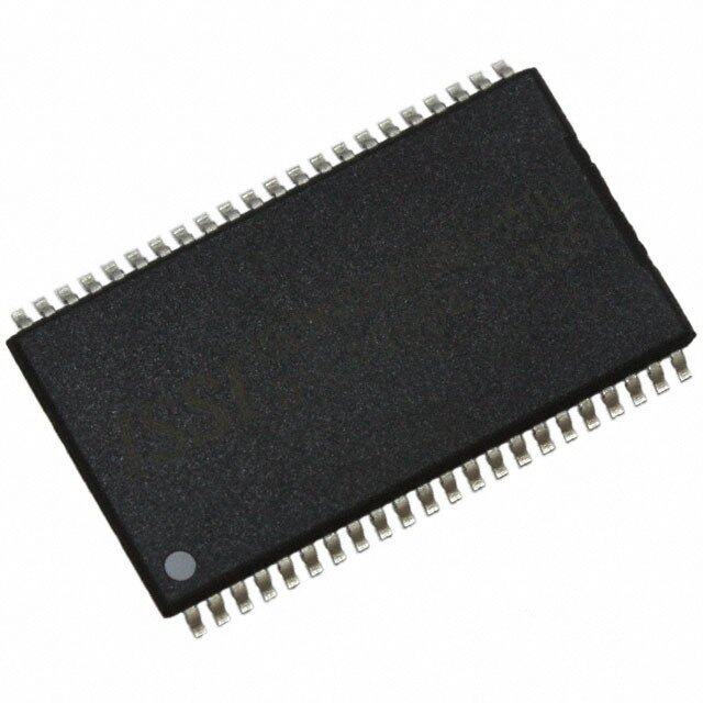
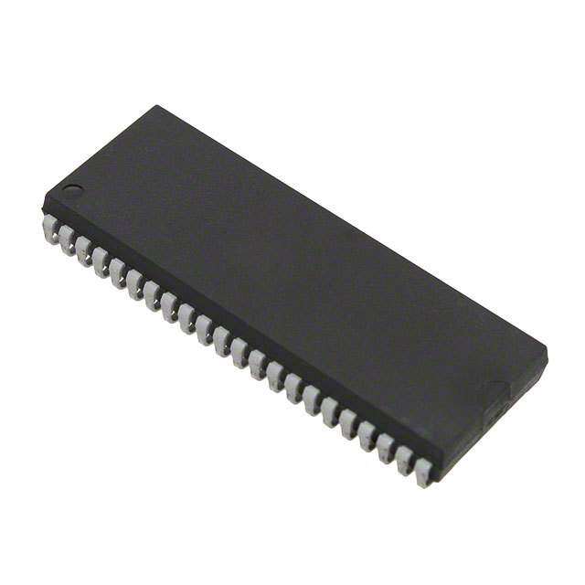
| 描述 | IC SRAM 256KBIT 15NS 28TSOP |
| 产品分类 | |
| 品牌 | Cypress Semiconductor Corp |
| 数据手册 | http://www.cypress.com/?docID=49198 |
| 产品图片 |
|
| 产品型号 | CY7C199NL-15ZXC |
| PCN组件/产地 | http://www.cypress.com/?docID=49741 |
| rohs | 无铅 / 符合限制有害物质指令(RoHS)规范要求 |
| 产品系列 | - |
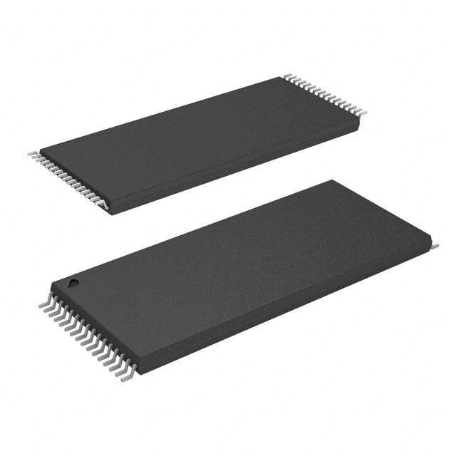
| 供应商器件封装 | 28-TSOP I |
| 其它名称 | CY7C199NL15ZXC |
| 包装 | 管件 |
| 存储器类型 | SRAM - 异步 |
| 存储容量 | 256K (32K x 8) |
| 封装/外壳 | 28-TSSOP (0.465", 11.80mm 宽) |
| 工作温度 | 0°C ~ 70°C |
| 接口 | 并联 |
| 标准包装 | 702 |
| 格式-存储器 | RAM |
| 电压-电源 | 4.5 V ~ 5.5 V |
| 速度 | 15ns |


- 商务部:美国ITC正式对集成电路等产品启动337调查
- 曝三星4nm工艺存在良率问题 高通将骁龙8 Gen1或转产台积电
- 太阳诱电将投资9.5亿元在常州建新厂生产MLCC 预计2023年完工
- 英特尔发布欧洲新工厂建设计划 深化IDM 2.0 战略
- 台积电先进制程称霸业界 有大客户加持明年业绩稳了
- 达到5530亿美元!SIA预计今年全球半导体销售额将创下新高
- 英特尔拟将自动驾驶子公司Mobileye上市 估值或超500亿美元
- 三星加码芯片和SET,合并消费电子和移动部门,撤换高东真等 CEO
- 三星电子宣布重大人事变动 还合并消费电子和移动部门
- 海关总署:前11个月进口集成电路产品价值2.52万亿元 增长14.8%


PDF Datasheet 数据手册内容提取
CY7C199N 32K × 8 Static RAM 32K × 8 Static RAM Features Functional Description ■High speed The CY7C199N is a high-performance CMOS static RAM ❐15 ns organized as 32,768 words by 8 bits. Easy memory expansion is provided by an active LOW Chip Enable (CE) and active LOW ■Fast tDOE Output Enable (OE) and three-state drivers. This device has an ■CMOS for optimum speed/power automatic power-down feature, reducing the power consumption by 81% when deselected. The CY7C199N is available in 28-pin ■Low active power TSOP I package. ❐550 mW (max, 15 ns “L” version) An active LOW Write Enable signal (WE) controls the ■Low standby power writing/reading operation of the memory. When CE and WE inputs are both LOW, data on the eight data input/output pins ❐0.275 mW (max, “L” version) (I/O through I/O ) is written into the memory location addressed 0 7 ■2 V data retention (“L” version only) by the address present on the address pins (A through A ). 0 14 Reading the device is accomplished by selecting the device and ■Easy memory expansion with CE and OE features enabling the outputs, CE and OE active LOW, while WE remains ■TTL-compatible inputs and outputs inactive or HIGH. Under these conditions, the contents of the location addressed by the information on address pins are ■Automatic power-down when deselected present on the eight data input/output pins. The input/output pins remain in a high-impedance state unless the chip is selected, outputs are enabled, and Write Enable (WE) is HIGH. A die coat is used to improve alpha immunity. For a complete list of related documentation, click here. Logic Block Diagram I/O0 INPUTBUFFER A0 I/O1 AAAAAAAA12345678 ROW DECODER 102A4RxR3A2Yx8 SENSE AMPS III///OOO234 A9 I/O5 WCEE COLUMN POWER I/O6 DECODER DOWN OE I/O7 10 11 12 13 14 A A A A A CypressSemiconductorCorporation • 198 Champion Court • SanJose, CA 95134-1709 • 408-943-2600 Document Number: 001-06493 Rev. *H Revised March 19, 2018
CY7C199N Contents Pin Configuration .............................................................3 Ordering Information ......................................................10 Selection Guide ................................................................3 Ordering Code Definitions .........................................10 Maximum Ratings .............................................................4 Package Diagrams ..........................................................11 Operating Range ...............................................................4 Acronyms ........................................................................12 Electrical Characteristics .................................................4 Document Conventions .................................................12 Capacitance ......................................................................5 Units of Measure .......................................................12 AC Test Loads and Waveforms .......................................5 Document History Page .................................................13 Data Retention Characteristics .......................................5 Sales, Solutions, and Legal Information ......................14 Data Retention Waveform ................................................5 Worldwide Sales and Design Support .......................14 Switching Characteristics ................................................6 Products ....................................................................14 Switching Waveforms ......................................................7 PSoC® Solutions ......................................................14 Typical DC and AC Characteristics ................................9 Cypress Developer Community .................................14 Truth Table ......................................................................10 Technical Support .....................................................14 Document Number: 001-06493 Rev. *H Page 2 of 14
CY7C199N Pin Configuration Figure 1. 28-pin TSOP 1 pinout OAE1 2223 2201 ACE0 A2 24 19 I/O7 A3 25 18 I/O6 WAE4 2267 TSOP I 1167 II//OO54 VCC 28 Top View 15 I/O3 A5 1 (not to scale) 14 GND A6 2 13 I/O2 AA87 43 1112 II//OO10 A9 5 10 A14 A10 6 9 A13 A11 7 8 A12 Selection Guide Description -15 Unit Maximum Access Time 15 ns Maximum Operating Current L 100 mA Maximum CMOS Standby Current L 0.05 mA Document Number: 001-06493 Rev. *H Page 3 of 14
CY7C199N Maximum Ratings DC Input Voltage [1] ............................–0.5 V to V + 0.5 V CC Output Current into Outputs (LOW) ............................20 mA Exceeding the maximum ratings may impair the useful life of the Static Discharge Voltage device. These user guidelines are not tested. (per MIL-STD-883, Method 3015) ......................... > 2001 V Storage Temperature ...............................–65 °C to +150 °C Latch-up Current ................................................... > 200 mA Ambient Temperature with Power Applied .........................................–55 °C to +125 °C Operating Range Supply Voltage to Ground Potential Range Ambient Temperature [2] V (Pin 28 to Pin 14) .........................................–0.5 V to +7.0 V CC Commercial 0 °C to +70 °C 5 V 10% DC Voltage Applied to Outputs in High Z State [1] ................................–0.5 V to V + 0.5 V CC Electrical Characteristics Over the Operating Range -15 Parameter Description Test Conditions Unit Min Max V Output HIGH Voltage V = Min, I = –4.0 mA 2.4 – V OH CC OH V Output LOW Voltage V = Min, I = 8.0 mA – 0.4 V OL CC OL V Input HIGH Voltage 2.2 V + 0.3 V IH CC V Input LOW Voltage –0.5 0.8 V IL I Input Load Current GND < V < V –5 +5 A IX I CC I Output Leakage Current GND < V < V , Output Disabled –5 +5 A OZ O CC I V Operating Supply Current V = Max, I = 0 mA, L – 100 mA CC CC CC OUT f = f = 1/t MAX RC I Automatic CE Power-down Max V , CE > V , L – 5 mA SB1 CC IH Current – TTL Inputs V > V or V < V , f = f IN IH IN IL MAX I Automatic CE Power-down Max V , L – 0.05 mA SB2 CC Current – CMOS Inputs CE > V – 0.3 V, CC V > V – 0.3 V, or V < 0.3 V, f = 0 IN CC IN Notes 1. VIL (min) = –2.0 V for pulse durations of less than 20 ns. 2. TA is the “instant on” case temperature. Document Number: 001-06493 Rev. *H Page 4 of 14
CY7C199N Capacitance Parameter [3] Description Test Conditions Max Unit C Input capacitance T = 25 C, f = 1 MHz, V = 5.0 V 8 pF IN A CC C Output capacitance 8 pF OUT AC Test Loads and Waveforms Figure 2. AC Test Loads and Waveforms [4] R1 481 R1 481 5 V 5 V ALL INPUT PULSES OUTPUT OUTPUT 3.0 V 90% 90% 10% 10% 30pF R2 5pF R2 GND 255 255 INCLUDING INCLUDING tr tr JIG AND JIG AND SCOPE (a) SCOPE (b) Equivalentto: THÉV ENIN EQUIVALENT 167 OUTPUT 1.73 V Data Retention Characteristics Over the Operating Range (L-version only) Parameter Description Conditions [5] Min Max Unit V V for Data Retention V = V = 2.0 V, 2.0 – V DR CC CC DR CE > V – 0.3 V, I Data Retention Current L CC – 10 A CCDR V > V – 0.3 V or IN CC tCDR[3] Chip Deselect to Data Retention Time VIN < 0.3 V 0 – ns t [4] Operation Recovery Time 200 – s R Data Retention Waveform Figure 3. Data Retention Waveform DATA RETENTION MODE VCC 3.0 V VDR> 2 V 3.0 V tCDR tR CE Notes 3. Tested initially and after any design or process changes that may affect these parameters. 4. tR< 3 ns for -15 speed. 5. No input may exceed VCC + 0.5 V. Document Number: 001-06493 Rev. *H Page 5 of 14
CY7C199N Switching Characteristics Over the Operating Range 7C199-15 Parameter [6] Description Unit Min Max Read Cycle t Read Cycle Time 15 – ns RC t Address to Data Valid – 15 ns AA t Data Hold from Address Change 3 – ns OHA t CE LOW to Data Valid – 15 ns ACE t OE LOW to Data Valid – 7 ns DOE t OE LOW to Low Z [7] 0 – ns LZOE t OE HIGH to High Z [7, 8] – 7 ns HZOE t CE LOW to Low Z [7] 3 – ns LZCE t CE HIGH to High Z [7, 8] – 7 ns HZCE t CE LOW to Power-up 0 – ns PU t CE HIGH to Power-down – 15 ns PD Write Cycle [9, 10] t Write Cycle Time 15 – ns WC t CE LOW to Write End 10 – ns SCE t Address Set-up to Write End 10 – ns AW t Address Hold from Write End 0 – ns HA t Address Set-up to Write Start 0 – ns SA t WE Pulse Width 9 – ns PWE t Data Set-up to Write End 9 – ns SD t Data Hold from Write End 0 – ns HD t WE LOW to High Z [7, 8] – 7 ns HZWE t WE HIGH to Low Z [7] 3 – ns LZWE Notes 6. Test conditions assume signal transition time of 3 ns or less for -15 speed, timing reference levels of 1.5 V, input pulse levels of 0 to 3.0 V, and output loading of the specified IOL/IOH and 30-pF load capacitance. 7. At any given temperature and voltage condition, tHZCE is less than tLZCE, tHZOE is less than tLZOE, and tHZWE is less than tLZWE for any given device. 8. tHZOE, tHZCE, and tHZWE are specified with CL = 5 pF as in part (b) of Figure 2 on page 5. Transition is measured 500 mV from steady-state voltage. 9. The internal write time of the memory is defined by the overlap of CE LOW and WE LOW. Both signals must be LOW to initiate a write and either signal can terminate a write by going HIGH. The data input set-up and hold timing should be referenced to the rising edge of the signal that terminates the write. 10.The minimum write cycle time for write cycle No. 3 (WE Controlled, OE LOW) is the sum of tHZWE and tSD. Document Number: 001-06493 Rev. *H Page 6 of 14
CY7C199N Switching Waveforms Figure 4. Read Cycle No. 1 [11, 12] tRC ADDRESS tAA tOHA DATA OUT PREVIOUS DATA VALID DATA VALID Figure 5. Read Cycle No. 2 [12, 13] tRC CE tACE OE tLZOEtDOE ttHHZZOCEE HIGH HIGH IMPEDANCE IMPEDANCE DATA OUT DATA VALID tLZCE tPU tPD VCC ICC SUPPLY 50% 50% CURRENT ISB Figure 6. Write Cycle No. 1 (WE Controlled) [14, 15, 16] tWC ADDRESS CE tAW tHA tSA tPWE WE OE tSD tHD DATA I/O DATAINVALID tHZOE Notes 11.Device is continuously selected. OE, CE = VIL. 12.WE is HIGH for read cycle. 13.Address valid prior to or coincident with CE transition LOW. 14.The internal write time of the memory is defined by the overlap of CE LOW and WE LOW. Both signals must be LOW to initiate a write and either signal can terminate a write by going HIGH. The data input set-up and hold timing should be referenced to the rising edge of the signal that terminates the write. 15.Data I/O is high impedance if OE = VIH. 16.If CE goes HIGH simultaneously with WE HIGH, the output remains in a high-impedance state. Document Number: 001-06493 Rev. *H Page 7 of 14
CY7C199N Switching Waveforms (continued) Figure 7. Write Cycle No. 2 (CE Controlled) [17, 18, 19] tWC ADDRESS CE tSCE tSA tAW tHA WE tSD tHD DATA I/O DATAINVALID Figure 8. Write Cycle No. 3 (WE Controlled, OE LOW) [19, 20] tWC ADDRESS CE tAW tHA tSA WE tSD tHD DATA I/O Note 21 DATAINVALID tHZWE tLZWE Notes 17.tHZOE, tHZCE, and tHZWE are specified with CL = 5 pF as in part (b) of Figure 2 on page 5. Transition is measured 500 mV from steady-state voltage. 18.Data I/O is high impedance if OE = VIH. 19.If CE goes HIGH simultaneously with WE HIGH, the output remains in a high-impedance state. 20.The minimum write cycle time for Write Cycle No. 3 (WE Controlled, OE LOW) is the sum of tHZWE and tSD. 21.During this period, the I/Os are in the output state. Do not apply input signals. Document Number: 001-06493 Rev. *H Page 8 of 14
CY7C199N Typical DC and AC Characteristics NORMALIZED SUPPLY CURRENT NORMALIZED SUPPLY CURRENT OUTPUT SOURCE CURRENT vs. S UPPLY VOLTAGE vs. AMBIENT TEMPERATURE A) vs. OUTPUT VOLTAGE 1.4 1.4 m120 , ICSB1.2 ICC , ICSB 1.2 ICC RENT (100 D I C1.0 D IC 1.0 UR 80 ZE 0.8 ZE 0.8 E C VCC = 5.0 V LI LI C 60 MA 0.6 VIN = 5.0 V MA 0.6 UR TA = 25 °C OR 0.4 TA = 25 °C OR 0.4 VCC = 5.0 V SO 40 N N V = 5.0 V T IN U 0.2 0.2 P 20 ISB ISB UT 0.0 0.0 O 0 4.0 4.5 5.0 5.5 6.0 –55 25 125 0.0 1.0 2.0 3.0 4.0 SUPPLY VOLTAGE (V) AMBIENT TEMPERATURE (C) OUTPUT VOLTAGE (V) NORMALIZED ACCESS TIME NORMALIZED ACCESS TIME OUTPUT SINK CURRENT vs. SUPPLY VOLTAGE vs. AMBIENT TEMPERATURE vs. OUTPUT VOLTAGE 1.4 1.6 A) 140 m T ( 120 ALIZED tAA 111...132 ALIZED tAA 11..42 K CURREN 18000 NORM 1.0 TA = 25 °C NORM 1.0 VCC = 5.0 V UT SIN 6400 VTAC C= =2 55 .°0C V P 0.8 T 0.9 U 20 O 0.8 0.6 0 4.0 4.5 5.0 5.5 6.0 –55 25 125 0.0 1.0 2.0 3.0 4.0 SUPPLY VOLTAGE (V) AMBIENT TEMPERATURE (C) OUTPUT VOLTAGE (V) TYPICAL POWER-ON CURRENT TYPICAL ACCESS TIME CHANGE vs. SUPPLY VOLTAGE vs. OUTPUT LOADING NORMALIZED ICC vs. CYCLE TIME 3.0 30.0 1.25 MALIZED IPO 221...505 LTA t (ns)AA 221505...000 MALIZED ICC1.00 VTVACIN C= = =2 055. .5°0C VV R E R NO 1.0 D 10.0 VCC = 4.5 V NO0.75 T = 25 °C A 0.5 5.0 0.0 0.0 0.50 0.0 1.0 2.0 3.0 4.0 5.0 0 200 400 600 800 1000 10 20 30 40 SUPPLY VOLTAGE (V) CAPACITANCE (pF) CYCLE FREQUENCY (MHz) Document Number: 001-06493 Rev. *H Page 9 of 14
CY7C199N Truth Table CE WE OE Inputs/Outputs Mode Power H X X High Z Deselect/Power-down Standby (I ) SB L H L Data Out Read Active (I ) CC L L X Data In Write Active (I ) CC L H H High Z Selected, Output disabled Active (I ) CC Ordering Information Speed Package Operating Package Type (ns) Ordering Code Diagram Range 15 CY7C199NL-15ZXC 51-85071 28-pin TSOP I (Pb-free) Commercial Contact your Local Cypress sales representative for availability of these parts Ordering Code Definitions CY 7 C 1 99 NL - 15 Z X C Temperature Range: C = Commercial Pb-free Package Type: Z = 28-pin TSOP I Speed: 15 ns NL = Low Power 99 = 256 Kbit density with data width × 8 bits Family Code: 1 = Fast Asynchronous SRAM family Technology Code: C = CMOS Marketing Code: 7 = SRAM Company ID: CY = Cypress Document Number: 001-06493 Rev. *H Page 10 of 14
CY7C199N Package Diagrams Figure 9. 28-pin TSOP I (8 × 13.4 × 1.2 mm) Package Outline, 51-85071 51-85071 *J Document Number: 001-06493 Rev. *H Page 11 of 14
CY7C199N Acronyms Document Conventions Units of Measure Acronym Description CE Chip Enable Symbol Unit of Measure CMOS Complementary Metal-Oxide Semiconductor °C degree Celsius I/O Input/Output MHz megahertz OE Output Enable µA microampere µs microsecond SOJ Small Outline J-lead mA milliampere SRAM Static Random Access Memory mW milliwatt TTL Transistor-Transistor Logic ns nanosecond TSOP Thin Small Outline Package ohm WE Write Enable % percent pF picofarad V volt W watt Document Number: 001-06493 Rev. *H Page 12 of 14
CY7C199N Document History Page Document Title: CY7C199N, 32K × 8 Static RAM Document Number: 001-06493 Orig. of Submission Rev. ECN No. Description of Change Change Date ** 423877 NXR 02/02/2006 New data sheet. *A 2892510 VKN 03/18/2010 Removed 12 ns, 20 ns, 25 ns, 35 ns, and 55 ns speed bins related information in all instances across the document. Removed Industrial and Military Temperature Range related information in all instances across the document. Removed 28-pin PDIP (300 Mils) package related information in all instances across the document. Updated Ordering Information: Updated part numbers. Updated Package Diagrams: spec 51-85071 – Changed revision from *G to *H. Removed spec 51-85014 *D. Updated to new template. *B 3109199 AJU 12/13/2010 Updated Ordering Information: No change in part numbers. Added Ordering Code Definitions. *C 3244591 PRAS 04/29/2011 Updated Package Diagrams: spec 51-85071 – Changed revision from *H to *I. Added Acronyms and Units of Measure. Updated to new template. Completing Sunset Review. *D 4379476 VINI 05/14/2014 Updated Switching Waveforms: Added Note 21 and referred the same note in DATA I/O in Figure8. Updated Package Diagrams: spec 51-85071 – Changed revision from *I to *J. Updated to new template. Completing Sunset Review. *E 4573121 VINI 11/18/2014 Updated Functional Description: Added “For a complete list of related documentation, click here.” at the end. *F 4776874 VINI 05/26/2015 Updated Functional Description: Updated description. Updated to new template. Completing Sunset Review. *G 5984694 AESATMP8 12/05/2017 Updated logo and Copyright. *H 6102775 VINI 03/19/2018 Updated to new template. Completing Sunset Review. Document Number: 001-06493 Rev. *H Page 13 of 14
CY7C199N Sales, Solutions, and Legal Information Worldwide Sales and Design Support Cypress maintains a worldwide network of offices, solution centers, manufacturer’s representatives, and distributors. To find the office closest to you, visit us at Cypress Locations. Products PSoC® Solutions Arm® Cortex® Microcontrollers cypress.com/arm PSoC 1 | PSoC 3 | PSoC 4 | PSoC 5LP | PSoC 6 MCU Automotive cypress.com/automotive Cypress Developer Community Clocks & Buffers cypress.com/clocks Community | Projects | Video | Blogs | Training | Components Interface cypress.com/interface Technical Support Internet of Things cypress.com/iot cypress.com/support Memory cypress.com/memory Microcontrollers cypress.com/mcu PSoC cypress.com/psoc Power Management ICs cypress.com/pmic Touch Sensing cypress.com/touch USB Controllers cypress.com/usb Wireless Connectivity cypress.com/wireless © Cypress Semiconductor Corporation, 2006-2018. This document is the property of Cypress Semiconductor Corporation and its subsidiaries, including Spansion LLC ("Cypress"). This document, including any software or firmware included or referenced in this document ("Software"), is owned by Cypress under the intellectual property laws and treaties of the United States and other countries worldwide. Cypress reserves all rights under such laws and treaties and does not, except as specifically stated in this paragraph, grant any license under its patents, copyrights, trademarks, or other intellectual property rights. If the Software is not accompanied by a license agreement and you do not otherwise have a written agreement with Cypress governing the use of the Software, then Cypress hereby grants you a personal, non-exclusive, nontransferable license (without the right to sublicense) (1) under its copyright rights in the Software (a) for Software provided in source code form, to modify and reproduce the Software solely for use with Cypress hardware products, only internally within your organization, and (b) to distribute the Software in binary code form externally to end users (either directly or indirectly through resellers and distributors), solely for use on Cypress hardware product units, and (2) under those claims of Cypress's patents that are infringed by the Software (as provided by Cypress, unmodified) to make, use, distribute, and import the Software solely for use with Cypress hardware products. Any other use, reproduction, modification, translation, or compilation of the Software is prohibited. TO THE EXTENT PERMITTED BY APPLICABLE LAW, CYPRESS MAKES NO WARRANTY OF ANY KIND, EXPRESS OR IMPLIED, WITH REGARD TO THIS DOCUMENT OR ANY SOFTWARE OR ACCOMPANYING HARDWARE, INCLUDING, BUT NOT LIMITED TO, THE IMPLIED WARRANTIES OF MERCHANTABILITY AND FITNESS FOR A PARTICULAR PURPOSE. To the extent permitted by applicable law, Cypress reserves the right to make changes to this document without further notice. Cypress does not assume any liability arising out of the application or use of any product or circuit described in this document. Any information provided in this document, including any sample design information or programming code, is provided only for reference purposes. It is the responsibility of the user of this document to properly design, program, and test the functionality and safety of any application made of this information and any resulting product. Cypress products are not designed, intended, or authorized for use as critical components in systems designed or intended for the operation of weapons, weapons systems, nuclear installations, life-support devices or systems, other medical devices or systems (including resuscitation equipment and surgical implants), pollution control or hazardous substances management, or other uses where the failure of the device or system could cause personal injury, death, or property damage ("Unintended Uses"). A critical component is any component of a device or system whose failure to perform can be reasonably expected to cause the failure of the device or system, or to affect its safety or effectiveness. Cypress is not liable, in whole or in part, and you shall and hereby do release Cypress from any claim, damage, or other liability arising from or related to all Unintended Uses of Cypress products. You shall indemnify and hold Cypress harmless from and against all claims, costs, damages, and other liabilities, including claims for personal injury or death, arising from or related to any Unintended Uses of Cypress products. Cypress, the Cypress logo, Spansion, the Spansion logo, and combinations thereof, WICED, PSoC, CapSense, EZ-USB, F-RAM, and Traveo are trademarks or registered trademarks of Cypress in the United States and other countries. For a more complete list of Cypress trademarks, visit cypress.com. Other names and brands may be claimed as property of their respective owners. Document Number: 001-06493 Rev. *H Revised March 19, 2018 Page 14 of 14