 Datasheet下载
- 型号: CY7C199CN-12VXA
- 制造商: Cypress Semiconductor
- 库位|库存: xxxx|xxxx
- 要求:
| 数量阶梯 | 香港交货 | 国内含税 |
| +xxxx | $xxxx | ¥xxxx |
查看当月历史价格
查看今年历史价格
CY7C199CN-12VXA产品简介:
ICGOO电子元器件商城为您提供CY7C199CN-12VXA由Cypress Semiconductor设计生产,在icgoo商城现货销售,并且可以通过原厂、代理商等渠道进行代购。 CY7C199CN-12VXA价格参考。Cypress SemiconductorCY7C199CN-12VXA封装/规格:存储器, SRAM - 异步 存储器 IC 256Kb (32K x 8) 并联 12ns 28-SOJ。您可以下载CY7C199CN-12VXA参考资料、Datasheet数据手册功能说明书,资料中有CY7C199CN-12VXA 详细功能的应用电路图电压和使用方法及教程。
| 参数 | 数值 |
| 产品目录 | 集成电路 (IC) |
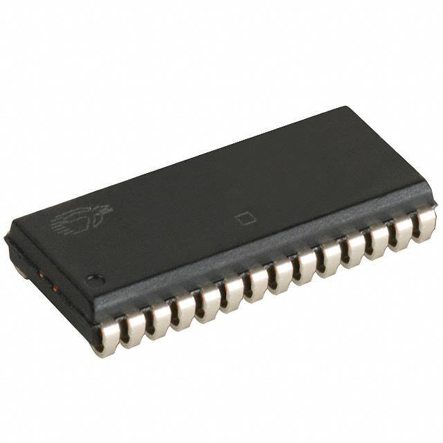
| 描述 | IC SRAM 256KBIT 12NS 28SOJ |
| 产品分类 | |
| 品牌 | Cypress Semiconductor Corp |
| 数据手册 | |
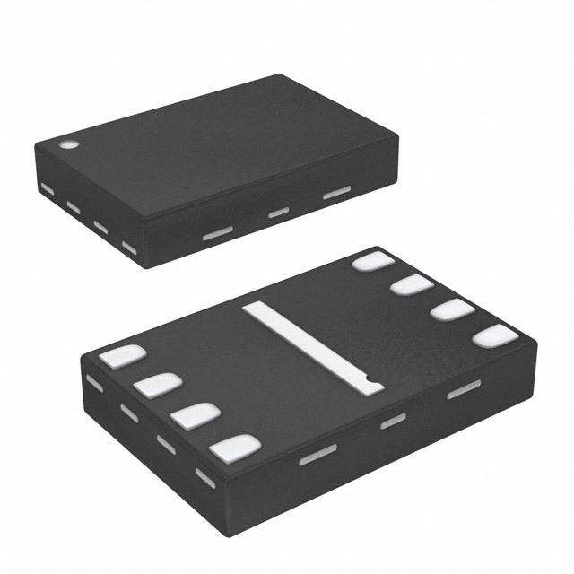
| 产品图片 |
|
| 产品型号 | CY7C199CN-12VXA |
| PCN过时产品 | http://www.cypress.com/?docID=44765 |
| rohs | 无铅 / 符合限制有害物质指令(RoHS)规范要求 |
| 产品系列 | - |
| 供应商器件封装 | 28-SOJ |
| 其它名称 | CY7C199CN12VXA |
| 包装 | 管件 |
| 存储器类型 | SRAM - 异步 |
| 存储容量 | 256K (32K x 8) |
| 封装/外壳 | 28-BSOJ |
| 工作温度 | -40°C ~ 85°C |
| 接口 | 并联 |
| 标准包装 | 27 |
| 格式-存储器 | RAM |
| 电压-电源 | 4.5 V ~ 5.5 V |
| 速度 | 12ns |


_renders/IS42S32800D-6BLI.jpg)


PDF Datasheet 数据手册内容提取
CY7C199CN 256K (32K x 8) Static RAM Features General Description [1] • Fast access time: 12 ns, 15 ns, 20 ns, and 25 ns The CY7C199CN is a high performance CMOS Asynchronous • Wide voltage range: 5.0V ± 10% (4.5V to 5.5V) SRAM organized as 32K by 8 bits that supports an asynchronous memory interface. The device features an • CMOS for optimum speed and power automatic power down feature that reduces power • TTL-compatible inputs and outputs consumption when deselected. • 2.0V data retention See the “Truth Table” on page3 in this data sheet for a • Low CMOS standby power complete description of read and write modes. • Automated power down when deselected The CY7C199CN is available in Pb-free 28-pin TSOPI, 28-pin • Available in Pb-free 28-pin TSOPI, 28-pin Molded SOJ and Molded SOJ and 28-pin DIP package(s). 28-pin DIP packages Logic Block Diagram Input Buffer er ps d m Deco RAM Array se A I/Ox w en o S R CE Column Decoder Power WE Down Circuit OE A X X Product Portfolio –12 –15 –20 –25 Unit Maximum Access Time 12 15 20 25 ns Maximum Operating Current 85 80 75 75 mA Maximum CMOS Standby Current 500 500 500 500 µA (low power) Note 1. For best practices recommendations, refer to the Cypress application note System Design Guidelines on www.cypress.com. CypressSemiconductorCorporation • 198 Champion Court • SanJose, CA 95134-1709 • 408-943-2600 Document #: 001-06435 Rev. *B Revised March 08, 2007
CY7C199CN Pin Layout and Specifications 28 DIP 28 SOJ A5 1 28 VCC A5 1 28 VCC A6 2 27 WE A6 2 27 WE A7 3 26 A4 A7 3 26 A4 A8 4 25 A3 A8 4 25 A3 A9 5 24 A2 A9 5 24 A2 A10 6 23 A1 A10 6 23 A1 A11 7 22 OE A11 7 22 OE A12 8 21 A0 A12 8 21 A0 A13 9 20 CE A13 9 20 CE A14 10 19 IO7 A14 10 19 IO7 IO0 11 18 IO6 IO0 11 18 IO6 IO1 12 17 IO5 IO1 12 17 IO5 IO2 13 16 IO4 IO2 13 16 IO4 VSS 14 15 IO3 VSS 14 15 IO3 OE 1 28 A0 A 2 27 CE 1 A2 3 26 IO7 A3 4 25 IO6 A4 5 24 IO5 WE 6 23 IO4 VCC 7 28 TSOP I (8 x 13.4 mm) 22 IO3 A5 8 21 VSS A6 9 20 IO2 A7 10 19 IO1 A8 11 18 IO0 A9 12 17 A14 A10 13 16 A13 A11 14 15 A12 Document #: 001-06435 Rev. *B Page 2 of 14
CY7C199CN Pin Description Pin Type Description DIP SOJ TSOP I A Input Address Inputs 1, 2, 3, 4, 5, 6, 7, 8, 9, 1, 2, 3, 4, 5, 6, 7, 8, 9, 2, 3, 4, 5, 8, 9, 10, 11, 12, X 10, 21, 23, 24, 25, 26 10, 21, 23, 24, 25, 26 13, 14, 15, 16, 17, 28 CE Control Chip Enable 20 20 27 IO Input or Output Data Input Outputs 11, 12, 13, 15, 16, 17, 11, 12, 13, 15, 16, 17, 18, 19, 20, 22, 23, 24, 25, X 18, 19 18, 19 26 OE Control Output Enable 22 22 1 V Supply Power (5.0V) 28 28 7 CC V Supply Ground 14 14 21 SS WE Control Write Enable 27 27 6 Truth Table CE OE WE IOx Mode Power H X X High-Z Deselect/Power Down Stand by (I ) SB L L H Data Out Read Active (I ) CC L X L Data In Write Active (I ) CC L H H High-Z Selected, Outputs Disabled Active (I ) CC Maximum Ratings Exceeding maximum ratings may impair the useful life of the device. These user guidelines are not tested. Parameter Description Value Unit T Storage Temperature –65 to +150 °C STG T Ambient Temperature with Power Applied (that is, case temperature) –55 to +125 °C AMB V Core Supply Voltage Relative to V –0.5 to +7.0 V CC SS V , V DC Voltage Applied to Any Pin Relative to V –0.5 to V + 0.5 V IN OUT SS CC I Output Short-Circuit Current 20 mA OUT V Static Discharge Voltage (in accordance with MIL-STD-883, Method 3015) > 2001 V ESD I Latch-up Current > 200 mA LU Operating Range Range Ambient Temperature (T ) Voltage Range (V ) A CC Commercial 0°C to 70°C 5.0V ± 10% Industrial –40°C to 85°C 5.0V ± 10% Automotive-A Document #: 001-06435 Rev. *B Page 3 of 14
CY7C199CN DC Electrical Characteristics Over the Operating Range (–12, –15) [2] –12 –15 Parameter Description Condition Power Unit Min Max Min Max V Input HIGH Voltage – 2.2 V + 0.3 2.2 V + 0.3 V IH CC CC V Input LOW Voltage – –0.5 0.8 –0.5 0.8 V IL V Output HIGH Voltage V = Min, I = –4.0 mA – 2.4 – 2.4 – V OH CC OH V Output LOW Voltage V = Min, I = 8.0 mA – – 0.4 – 0.4 V OL CC OL I V Operating V = Max, I = 0 mA, – – 85 – 80 mA CC CC CC OUT Supply Current f = F = 1/t max RC I Automatic CE Power Max V , CE ≥ V , – – 30 – 30 mA SB1 CC IH Down Current TTL V ≥ V or V ≤ V , f = F IN IH IN IL max Inputs L – 10 – 10 mA I Automatic CE Power Max V , CE ≥ V – 0.3V, – – 10 – 10 mA SB2 CC CC Down Current CMOS V ≥ V – 0.3V, or V ≤ 0.3V, f = 0 IN CC IN Inputs L – 500 – 500 µA I Output Leakage GND ≤ V ≤ V , Output Disabled – –5 +5 –5 +5 µA OZ I CC Current I Input Leakage GND ≤ V ≤ V – –5 +5 –5 +5 µA IX I CC Current DC Electrical Characteristics Over the Operating Range (–20, –25) [2] –20 –25 Parameter Description Condition Power Unit Min Max Min Max V Input HIGH Voltage – 2.2 V + 0.3 2.2 V + 0.3 V IH CC CC V Input LOW Voltage – –0.5 0.8 –0.5 0.8 V IL V Output HIGH Voltage V = Min, I = –4.0 mA – 2.4 – 2.4 – V OH CC OH V Output LOW Voltage V = Min, I = 8.0 mA – – 0.4 – 0.4 V OL CC OL I V Operating V = Max, I = 0 mA, – – 75 – 75 mA CC CC CC OUT Supply Current f = F = 1/t max RC I Automatic CE Power Max V , CE ≥ V , – – 30 – 30 mA SB1 CC IH Down Current TTL V ≥ V or V ≤ V , f = F IN IH IN IL max Inputs L – 10 – 10 mA I Automatic CE Power Max V , CE ≥ V – 0.3V, – – 10 – 10 mA SB2 CC CC Down Current CMOS V ≥ V – 0.3V, or V ≤ 0.3V, f = 0 IN CC IN Inputs L – 500 – 500 µA I Output Leakage GND ≤ Vi ≤ V , Output Disabled – –5 +5 –5 +5 µA OZ CC Current I Input Leakage GND ≤ Vi ≤ V – –5 +5 –5 +5 µA IX CC Current Note 2. VIL (min) = –2.0V for pulse durations of less than 20 ns. Document #: 001-06435 Rev. *B Page 4 of 14
CY7C199CN Capacitance [3] Parameter Description Conditions Max Unit C Input Capacitance T = 25°C, f = 1 MHz, V = 5.0V 8 pF IN A CC C Output Capacitance 8 OUT Thermal Resistance [3] Parameter Description Conditions TSOP I SOJ DIP Unit Θ Thermal Resistance Still air, soldered on a 3 × 4.5 88.6 79 69.33 °C/W JA (junction to ambient) square inch, two–layer printed circuit board Θ Thermal Resistance 21.94 41.42 31.62 JC (junction to case) AC Test Loads Output Loads Output Loads for t ,t &t R1 HZOE HZCE HZWE R3 VCC VCC Output C1 R2 C2 R4 (A)* (B)* All Input Pulses Thevenin Equivalent VCC 90% 90% Output Rth VT VSS 10% 10% Rise Time Fall Time 1 V/ns 1 V/ns * including scope and jig capacitance AC Test Conditions Parameter Description Nom Unit C1 Capacitor 1 30 pF C2 Capacitor 2 5 R1 Resistor 1 480 Ω R2 Resistor 2 255 R3 Resistor 3 480 R4 Resistor 4 255 R Resistor Thevenin 167 TH V Voltage Thevenin 1.73 V TH Note 3. Tested initially and after any design or process change that may affect these parameters. Document #: 001-06435 Rev. *B Page 5 of 14
CY7C199CN AC Electrical Characteristics [4] –12 –15 –20 –25 Parameter Description Unit Min Max Min Max Min Max Min Max t Read Cycle Time 12 – 15 – 20 – 25 – ns RC t Address to Data Valid – 12 – 15 – 20 – 25 ns AA t Data Hold from Address 3 – 3 – 3 – 3 – ns OHA Change t CE to Data Valid – 12 – 15 – 20 – 25 ns ACE t OE to Data Valid Ind’l/Com’l – 5 – 7 – 9 – 9 ns DOE Automotive-A – 6 – – – – – – t OE to Low-Z [5] 0 – 0 – 0 – 0 – ns LZOE t OE to High-Z [5, 6] – 5 – 7 – 9 – 9 ns HZOE t CE to Low-Z [5] 3 – 3 – 3 – 3 – ns LZCE t CE to High-Z [5, 6] – 5 – 7 – 9 – 9 ns HZCE t CE to Power Up 0 – 0 – 0 – 0 – ns PU t CE to Power Down – 12 – 15 – 20 – 20 ns PD t Write Cycle Time [7] 12 – 15 – 20 – 25 – ns WC t CE to Write End 9 – 10 – 15 – 15 – ns SCE t Address Setup to Write End 9 – 10 – 15 – 15 – ns AW t Address Hold from Write End 0 – 0 – 0 – 0 – ns HA t Address Setup to Write Start 0 – 0 – 0 – 0 – ns SA t WE Pulse Width 8 – 9 – 15 – 15 – ns PWE t Data Setup to Write End 8 – 9 – 10 – 10 – ns SD t Data Hold from Write End 0 – 0 – 0 – 0 – ns HD t WE LOW to High-Z [5, 6] – 7 – 7 – 10 – 10 ns HZWE t WE HIGH to Low-Z [5] 3 – 3 – 3 – 3 – ns LZWE Data Retention Characteristics [8] Parameter Description Condition Min Max Unit V V for Data Retention 2.0 – V DR CC I Data Retention Current V = V = 2.0V, CE ≥ V – 0.3V, – 150 µA CCDR CC DR CC V ≥ V – 0.3V or V ≤ 0.3V t Chip Deselect to Data IN CC IN 0 – ns CDR Retention Time t Operation Recovery Time 200 – µs R Notes 4. Test Conditions are based on a transition time of 3 ns or less and timing reference levels of 1.5V, and input pulse levels of 0 to 3.0V. 5. At any given temperature and voltage condition, tHZCE is less than tLZCE, tHZOE is less than tLZOE, and tHZWE is less than tLZWE for any given device. 6. tHZOE, tHZCE, tHZWE are specified as in part (b) of the “” on page1. Transitions are measured ± 200 mV from steady state voltage. 7. The internal memory write time is defined by the overlap of CE LOW and WE LOW. CE and WE must be LOW to initiate a write, and the transition of any of these signals can terminate the write. The input data setup and hold timing must be referenced to the leading edge of the signal that terminates the write. 8. L-version only. Document #: 001-06435 Rev. *B Page 6 of 14
CY7C199CN Timing Waveforms Data Retention Waveform V DATA RETENTION MODE CC t t CDR R CE Read Cycle 1 [9, 10] t RC Address t AA t OHA Data Out Previous Data Valid Data Valid Read Cycle 2 [11, 12] t RC Address CE t t HZCE ACE OE t t DOE HZOE t LZOE High Z High Z Data Out Data Valid t LZCE t t I PU PD CC V CC I 50% 50% SB Current Notes 9. Device is continuously selected. OE = VIL = CE. 10.WE is HIGH for read cycle. 11.This cycle is OE controlled and WE is HIGH read cycle. 12.Address valid before or similar with CE transition LOW. Document #: 001-06435 Rev. *B Page 7 of 14
CY7C199CN Timing Waveforms (continued) Write Cycle 1 (WE controlled) [13, 14, 15] t WC Address t SCE CE tAW tHA tSA tPWE WE OE t HD t t HZOE SD Data In/Out Undefined Data-In Valid see footnotes Write Cycle 2 (CE controlled) [14, 16, 17] t WC Address t SCE CE t t SA HA t AW WE tSD tHD High Z High Z Data In/Out Data-In Valid Notes 13. This cycle is WE controlled, OE is HIGH during write. 14. Data in and/or out is high impedance if OE = VIH. 15. During this period the IOs are in output state and input signals must not be applied. 16.This cycle is CE controlled. 17. If CE goes HIGH simultaneously with WE going HIGH, the output remains in a high impedance state. Document #: 001-06435 Rev. *B Page 8 of 14
CY7C199CN Timing Waveforms (continued) Write Cycle 3 (WE controlled, OE low) [18] t WC Address t SCE CE tAW tHA tSA tPWE WE t t HD SD Data Undefined Data In Valid Undefined In Out see footnotes See Footnotes t t HZWE LZWE Note 18.The cycle is WE controlled, OE LOW. The minimum write cycle time is the sum of tHZWE and tSD. Document #: 001-06435 Rev. *B Page 9 of 14
CY7C199CN Ordering Information Contact local sales representative regarding availability of these parts. Speed Package Power Op- Operating Ordering Code Package Type (ns) Diagram tion Range 12 CY7C199CN–12VC 51-85031 28-Lead (300-Mil) Molded SOJ Standard Commercial CY7C199CN–12ZC 51-85071 28 TSOP I (8 x 13.4 mm) Standard Commercial CY7C199CN–12ZXC 51-85071 28 TSOP I (8 x 13.4 mm), Pb-free Standard Commercial CY7C199CN–12VI 51-85031 28-Lead (300-Mil) Molded SOJ Standard Industrial CY7C199CN–12VXI 51-85031 28-Lead (300-Mil) Molded SOJ, Pb-free Standard Industrial CY7C199CN–12VXA 51-85031 28-Lead (300-Mil) Molded SOJ, Pb-free Standard Automotive-A 15 CY7C199CN–15PC 51-85014 28 DIP (6.9 x 35.6 x 3.5 mm) Standard Commercial CY7C199CN–15PXC 51-85014 28 DIP (6.9 x 35.6 x 3.5 mm), Pb-free Standard Commercial CY7C199CN–15VC 51-85031 28-Lead (300-Mil) Molded SOJ Standard Commercial CY7C199CN–15VXC 51-85031 28-Lead (300-Mil) Molded SOJ, Pb-free Standard Commercial CY7C199CN–15ZC 51-85071 28 TSOP I (8 x 13.4 mm), Pb-free Standard Commercial CY7C199CN–15ZXC 51-85071 28 TSOP I (8 x 13.4 mm), Pb-free Standard Commercial CY7C199CN–15VI 51-85031 28-Lead (300-Mil) Molded SOJ Standard Industrial CY7C199CNL–15VC 51-85031 28-Lead (300-Mil) Molded SOJ Low Power Commercial CY7C199CNL–15VXC 51-85031 28-Lead (300-Mil) Molded SOJ, Pb-free Low Power Commercial CY7C199CNL–15ZXC 51-85071 28 TSOP I (8 x 13.4 mm), Pb-free Low Power Commercial CY7C199CNL–15VXI 51-85031 28-Lead (300-Mil) Molded SOJ, Pb-free Low Power Industrial 20 CY7C199CN–20VC 51-85031 28-Lead (300-Mil) Molded SOJ Standard Commercial CY7C199CN–20ZI 51-85071 28 TSOP I (8 x 13.4 mm) Standard Industrial CY7C199CN–20ZXI 51-85071 28 TSOP I (8 x 13.4 mm), Pb-free Standard Industrial 25 CY7C199CN–25PC 51-85014 28 DIP (6.9 x 35.6 x 3.5 mm) Standard Commercial CY7C199CN–25PXC 51-85014 28 DIP (6.9 x 35.6 x 3.5 mm), Pb-free Standard Commercial Document #: 001-06435 Rev. *B Page 10 of 14
CY7C199CN Package Diagrams Figure 1. 28-pin TSOP I (8 x 13.4 mm), 51-85071 51-85071-*G Document #: 001-06435 Rev. *B Page 11 of 14
CY7C199CN Package Diagrams (continued) Figure 2. 28-pin (300 Mil) Molded SOJ, 51-85031 NOTE: 1.JEDECSTDREFMO088 2.BODYLENGTHDIMENSIONDOESNOTINCLUDEMOLDPROTRUSION/ENDFLASH MOLDPROTRUSION/ENDFLASHSHALLNOTEXCEED0.006in(0.152mm)PERSIDE 3.DIMENSIONSININCHES MIN. MAX. DETAIL A PIN1ID EXTERNALLEADDESIGN 14 1 0.291 0.330 0.300 0.350 0.026 0.032 0.013 15 28 0.019 0.014 0.020 OPTION1 OPTION2 0.697 SEATINGPLANE 0.713 0.120 0.140 0.007 0.013 A 0.004 0.262 0.050 TYP. 0.025MIN. 0.272 51-85031-*C Document #: 001-06435 Rev. *B Page 12 of 14
CY7C199CN Package Diagrams (continued) Figure 3. 28-pin (300 Mil) PDIP, 51-85014 SEELEADENDOPTION 14 1 DIMENSIONSININCHES[MM]MIN. MAX. REFERENCEJEDECMO-095 0.260[6.60] 0.295[7.49] PACKAGEWEIGHT:2.15gms 15 28 0.030[0.76] 0.080[2.03] SEATINGPLANE 1.345[34.16] 1.385[35.18] 0.290[7.36] 0.325[8.25] 00..114900[[34..5852]] 00..112400[[33..0555]] 00..111650[[24..9026]] 0.015[0.38] 00..000192[[00..2330]] 3°MIN. 0.060[1.52] 0.055[1.39] 0.310[7.87] 0.090[2.28] 0.065[1.65] 0.385[9.78] 0.110[2.79] 0.015[0.38] 0.020[0.50] SEELEADENDOPTION LEADENDOPTION 51-85014-*D (LEAD#1,14,15&28) All product and company names mentioned in this document may be the trademarks of their respective holders. Document #: 001-06435 Rev. *B Page 13 of 14 © Cypress Semiconductor Corporation, 2006-2007. The information contained herein is subject to change without notice. Cypress Semiconductor Corporation assumes no responsibility for the use of any circuitry other than circuitry embodied in a Cypress product. Nor does it convey or imply any license under patent or other rights. Cypress products are not warranted nor intended to be used for medical, life support, life saving, critical control or safety applications, unless pursuant to an express written agreement with Cypress. Furthermore, Cypress does not authorize its products for use as critical components in life-support systems where a malfunction or failure may reasonably be expected to result in significant injury to the user. The inclusion of Cypress products in life-support systems application implies that the manufacturer assumes all risk of such use and in doing so indemnifies Cypress against all charges.
CY7C199CN Document History Page Document Title: CY7C199CN, 256K (32K x 8) Static RAM Document Number: 001-06435 Issue Orig. of REV. ECN No. Description of Change Date Change ** 430363 See ECN NXR New Data Sheet *A 684342 See ECN VKN Added Automotive-A Information Updated Ordering Information Table *B 839904 See ECN VKN Added t spec for Automotive-A part in AC Electrical characteristics DOE table Document #: 001-06435 Rev. *B Page 14 of 14