
 Datasheet下载
- 型号: CY7C1021BN-15ZSXE
- 制造商: Cypress Semiconductor
- 库位|库存: xxxx|xxxx
- 要求:
| 数量阶梯 | 香港交货 | 国内含税 |
| +xxxx | $xxxx | ¥xxxx |
查看当月历史价格
查看今年历史价格
CY7C1021BN-15ZSXE产品简介:
ICGOO电子元器件商城为您提供CY7C1021BN-15ZSXE由Cypress Semiconductor设计生产,在icgoo商城现货销售,并且可以通过原厂、代理商等渠道进行代购。 CY7C1021BN-15ZSXE价格参考¥25.18-¥26.32。Cypress SemiconductorCY7C1021BN-15ZSXE封装/规格:存储器, SRAM - 异步 存储器 IC 1Mb (64K x 16) 并联 15ns 44-TSOP II。您可以下载CY7C1021BN-15ZSXE参考资料、Datasheet数据手册功能说明书,资料中有CY7C1021BN-15ZSXE 详细功能的应用电路图电压和使用方法及教程。
| 参数 | 数值 |
| 产品目录 | 集成电路 (IC)半导体 |
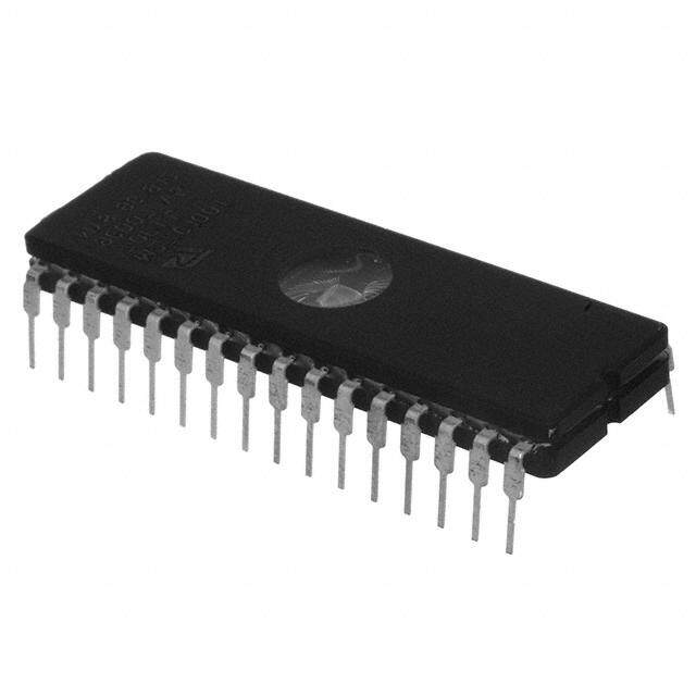
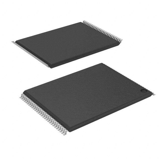
| 描述 | IC SRAM 1MBIT 15NS 44TSOP静态随机存取存储器 2Mb 15ns 64K x 16 Fast Async 静态随机存取存储器 |
| 产品分类 | |
| 品牌 | Cypress Semiconductor |
| 产品手册 | |
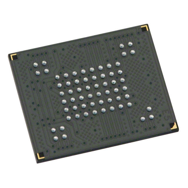
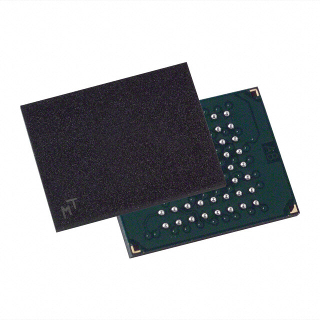
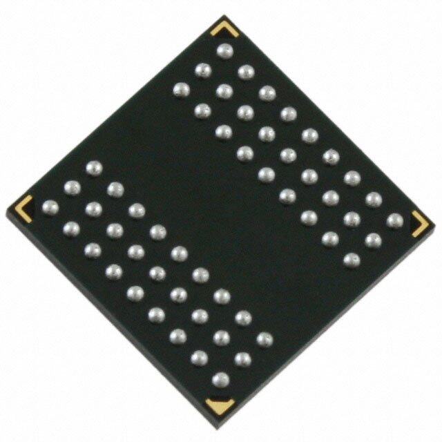
| 产品图片 |
|
| rohs | 符合RoHS无铅 / 符合限制有害物质指令(RoHS)规范要求 |
| 产品系列 | 内存,静态随机存取存储器,Cypress Semiconductor CY7C1021BN-15ZSXE- |
| 数据手册 | http://www.cypress.com/?docID=45953 |
| 产品型号 | CY7C1021BN-15ZSXE |
| 产品种类 | 静态随机存取存储器 |
| 供应商器件封装 | 44-TSOP II |
| 其它名称 | CY7C1021BN15ZSXE |
| 包装 | 托盘 |
| 商标 | Cypress Semiconductor |
| 存储器类型 | SRAM - 异步 |
| 存储容量 | 1 Mbit |
| 存储类型 | SDR |
| 安装风格 | SMD/SMT |
| 封装 | Tray |
| 封装/外壳 | 44-TSOP(0.400",10.16mm 宽) |
| 封装/箱体 | TSOP-II-44 |
| 工作温度 | -40°C ~ 125°C |
| 工厂包装数量 | 135 |
| 接口 | Parallel |
| 最大工作温度 | + 125 C |
| 最大工作电流 | 130 mA |
| 最小工作温度 | - 40 C |
| 标准包装 | 135 |
| 格式-存储器 | RAM |
| 电压-电源 | 4.5 V ~ 5.5 V |
| 电源电压-最大 | 5.5 V |
| 电源电压-最小 | 4.5 V |
| 类型 | Asynchronous |
| 系列 | CY7C1021BN |
| 组织 | 64 k x 16 |
| 访问时间 | 15 ns |
| 速度 | 15ns |


- 商务部:美国ITC正式对集成电路等产品启动337调查
- 曝三星4nm工艺存在良率问题 高通将骁龙8 Gen1或转产台积电
- 太阳诱电将投资9.5亿元在常州建新厂生产MLCC 预计2023年完工
- 英特尔发布欧洲新工厂建设计划 深化IDM 2.0 战略
- 台积电先进制程称霸业界 有大客户加持明年业绩稳了
- 达到5530亿美元!SIA预计今年全球半导体销售额将创下新高
- 英特尔拟将自动驾驶子公司Mobileye上市 估值或超500亿美元
- 三星加码芯片和SET,合并消费电子和移动部门,撤换高东真等 CEO
- 三星电子宣布重大人事变动 还合并消费电子和移动部门
- 海关总署:前11个月进口集成电路产品价值2.52万亿元 增长14.8%

_renders/MR4A16BCYS35.jpg)
PDF Datasheet 数据手册内容提取
CY7C1021BN 1-Mbit (64 K × 16) Static RAM 1-Mbit (64 K × 16) Static RAM Features Functional Description ■Temperature ranges The CY7C1021BN is a high performance CMOS static RAM ❐Commercial: 0 °C to 70 °C organized as 65,536 words by 16 bits. This device has an ❐Industrial: –40 °C to 85 °C automatic power down feature that significantly reduces power consumption when deselected. ❐Automotive-A: –40 °C to 85 °C ❐Automotive-E: –40 °C to 125 °C Writing to the device is accomplished by taking Chip Enable (CE) and Write Enable (WE) inputs LOW. If Byte Low Enable (BLE) is ■High speed LOW, then data from the input/output (I/O) pins (I/O through 1 ❐tAA = 15 ns (Automotive) I/O8), is written into the location specified on the address pins (A0 ■Complementary metal oxide semiconductor (CMOS) for through A15). If Byte High Enable (BHE) is LOW, then data from optimum speed/power I/O pins (I/O9 through I/O16) is written into the location specified on the address pins (A through A ). 0 15 ■Low active power Reading from the device is accomplished by taking CE and ❐825 mW (maximum) Output Enable (OE) LOW while forcing WE HIGH. If BLE is LOW, ■Automatic power down when deselected then data from the memory location specified by the address pins appears on I/O to I/O . If BHE is LOW, then data from memory 1 8 ■Independent control of upper and lower bits appears on I/O to I/O . See the Truth Table on page 11 for a 9 16 complete description of read and write modes. ■Available in Pb-free and non Pb-free 44-pin TSOP II and 44-pin 400-mil-wide SOJ The I/O pins (I/O through I/O ) are placed in a high impedance 1 16 state when the device is deselected (CE HIGH), the outputs are disabled (OE HIGH), the BHE and BLE are disabled (BHE, BLE HIGH), or during a write operation (CE LOW, WE LOW). The CY7C1021BN is available in standard 44-pin TSOP type II and 44-pin 400-mil-wide SOJ packages. Use part number CY7C1021BN when ordering 15 ns t . AA For a complete list of related resources, click here. Logic Block Diagram Data In Drivers A 7 AAAAA24356 Row Decoder 5R16A24M KX A x2 r10ra64y8 Sense Amps II//OO19––II//OO816 A 1 A 0 Column Decoder BHE WE A8A9A10A11A12A13A14A15 CE OE BLE CypressSemiconductorCorporation • 198 Champion Court • SanJose, CA 95134-1709 • 408-943-2600 Document Number: 001-06494 Rev. *J Revised November 29, 2017
CY7C1021BN Contents Selection Guide ................................................................3 Package Diagrams ..........................................................13 Pin Configuration .............................................................3 Acronyms ........................................................................14 Pin Definitions ..................................................................4 Document Conventions .................................................14 Maximum Ratings .............................................................5 Units of Measure .......................................................14 Operating Range ...............................................................5 Document History Page .................................................15 Electrical Characteristics .................................................5 Sales, Solutions, and Legal Information ......................16 Capacitance ......................................................................6 Worldwide Sales and Design Support .......................16 Thermal Resistance ..........................................................6 Products ....................................................................16 AC Test Loads and Waveforms .......................................6 PSoC® Solutions ......................................................16 Switching Characteristics ................................................7 Cypress Developer Community .................................16 Switching Waveforms ......................................................8 Technical Support .....................................................16 Truth Table ......................................................................11 Ordering Information ......................................................12 Ordering Code Definitions .........................................12 Document Number: 001-06494 Rev. *J Page 2 of 16
CY7C1021BN Selection Guide Description CY7C1021B-15 Maximum access time (ns) 15 Maximum operating current (mA) Commercial/Industrial 130 Automotive-A 130 Automotive-E 130 Maximum CMOS standby current (mA) Commercial/Industrial 10 Commercial/Industrial (L version) 0.5 Automotive-A (L version) 0.5 Automotive-E 15 Pin Configuration Figure 1. 44-pin SOJ/TSOP II pinout (Top View) A4 1 44 A5 A3 2 43 A6 A2 3 42 A7 A1 4 41 OE A0 5 40 BHE CE 6 39 BLE I/O1 7 38 I/O16 I/O2 8 37 I/O15 I/O3 9 36 I/O14 I/O4 10 35 I/O13 VCC 11 34 VSS VSS 12 33 VCC I/O5 13 32 I/O12 I/O6 14 31 I/O11 I/O7 15 30 I/O10 I/O8 16 29 I/O9 WE 17 28 NC A15 18 27 A8 A14 19 26 A9 A13 20 25 A10 A12 21 24 A11 NC 22 23 NC Document Number: 001-06494 Rev. *J Page 3 of 16
CY7C1021BN Pin Definitions Pin Name Pin Number I/O Type Description A –A 1–5,18–21, Input Address inputs used to select one of the address locations. 0 15 24–27, 42–44 I/O –I/O 7–10, 13–16, Input/Output Bidirectional data I/O lines. Used as input or output lines depending on operation. 1 16 29–32, 35–38 NC 22, 23, 28 No Connect Not connected to the die. WE 17 Input/Control Write enable input, active LOW. When selected LOW, a write is conducted. When deselected HIGH, a read is conducted. CE 6 Input/Control Chip enable input, active LOW. When LOW, selects the chip. When HIGH, deselects the chip. BHE, BLE 40, 39 Input/Control Byte enable select inputs, active LOW. BHE controls I/O –I/O ,BLE controls I/O –I/O . 16 9 8 1 OE 41 Input/Control Output enable, active LOW. Controls the direction of the I/O pins. When LOW, the I/O pins are allowed to behave as outputs. When deasserted HIGH, I/O pins are tristated, and act as input data pins. V 12, 34 Ground Ground for the device. Should be connected to ground of the system. SS V 11, 33 Power Supply Power supply inputs to the device. CC Document Number: 001-06494 Rev. *J Page 4 of 16
CY7C1021BN Maximum Ratings Current into outputs (LOW) ........................................20 mA Static discharge voltage Exceeding the maximum ratings may impair the useful life of the (per MIL-STD-883, Method 3015) ..........................> 2001 V device. These user guidelines are not tested. Latch-up current ....................................................> 200 mA Storage temperature ................................–65 C to +150 C Ambient temperature with Operating Range power applied ..........................................–55C to +125 C Supply voltage on Range Ambient Temperature (TA)[2] VCC V relative to GND [1] ................................–0.5 V to +7.0 V CC Commercial 0 C to +70 C 5 V 10% DC voltage applied to outputs in High Z state [1] ................................–0.5 V to V + 0.5 V Industrial –40 C to +85 C CC DC input voltage [1] .............................–0.5 V to V + 0.5 V Automotive-A –40 C to +85 C CC Automotive-E –40 C to +125 C Electrical Characteristics Over the operating range -15 Parameter Description Test Conditions Unit Min Max V Output HIGH voltage V = Min, I = –4.0 mA 2.4 – V OH CC OH V Output LOW voltage V = Min, I = 8.0 mA – 0.4 V OL CC OL V Input HIGH voltage 2.2 6.0 V IH V Input LOW voltage[1] –0.5 0.8 V IL I Input leakage current GND < V < V Commercial / Industrial –1 +1 A IX I CC Automotive-A –1 +1 A Automotive-E –4 +4 A I Output leakage current GND < V < V , Commercial / Industrial –1 +1 A OZ I CC Output Disabled Automotive-A –1 +1 A Automotive-E –4 +4 A I V operating supply current V = Max, Commercial / Industrial – 130 mA CC CC CC I = 0 mA, OUT Automotive-A – 130 f = f = 1/t MAX RC Automotive-E – 130 I Automatic CE power down Max V , CE > V , Commercial / Industrial – 40 mA SB1 CC IH current – TTL inputs V > V or V < V , IN IH IN IL Automotive-A – 40 f = f MAX Automotive-E – 50 I Automatic CE power down Max V , Commercial / Industrial – 10 mA SB2 CC current – CMOS inputs CE > V – 0.3 V, CC Commercial / Industrial (L) – 0.5 V > V – 0.3 V, IN CC or V < 0.3 V, f = 0 Automotive-A (L) – 0.5 IN Automotive-E – 15 Notes 1. VIL (min.) = –2.0 V and VIH(max) = VCC + 0.5 V for pulse durations of less than 20 ns. 2. TA is the “Instant On” case temperature. Document Number: 001-06494 Rev. *J Page 5 of 16
CY7C1021BN Capacitance Parameter [3] Description Test Conditions Max Unit C Input capacitance T = 25 C, f = 1 MHz, V = 5.0 V 8 pF IN A CC C Output capacitance 8 pF OUT Thermal Resistance Parameter [3] Description Test Conditions 44-pin SOJ 44-pin TSOP II Unit Thermal resistance Test conditions follow standard test 64.32 76.89 C/W JA (junction to ambient) methods and procedures for measuring Thermal resistance thermal impedance, per EIA / JESD51. 31.03 14.28 C/W JC (junction to case) AC Test Loads and Waveforms Figure 2. AC Test Loads and Waveforms R 481 R 481 AALLLL IINNPPUUTT PPUULLSSEESS 5 V 5 V 3.0 V 9900%% 9900%% OOUUTTPPUUTT OOUUTTPPUUTT 1100%% 1100%% 3300 ppFF RR22 55 ppFF RR22 GGNNDD 255 255 IINNCCLLUUDDIINNGG IINNCCLLUUDDIINNGG JJIIGG AANNDD JJIIGG AANNDD RRiissee TTiimmee:: 11 VV//nnss Fall Time: 1 V/ns SSCCOOPPEE ((aa)) SSCCOOPPEE ((bb)) 116677 EEqquuiivvaalleenntt ttoo:: TTHHÉÉVVEENNIINN OOUUTTPPUUTT 1.73 V EEQQUUIIVVAALLEENNTT 3300 ppFF Note 3. Tested initially and after any design or process changes that may affect these parameters. Document Number: 001-06494 Rev. *J Page 6 of 16
CY7C1021BN Switching Characteristics Over the operating range -15 Parameter [4] Description Unit Min Max Read Cycle t Read cycle time 15 – ns RC t Address to data valid – 15 ns AA t Data hold from address change 3 – ns OHA t CE LOW to data valid – 15 ns ACE t OE LOW to data valid – 7 ns DOE t OE LOW to low Z[4] 0 – ns LZOE t OE HIGH to high Z[5, 6] – 7 ns HZOE t CE LOW to low Z[5] 3 – ns LZCE t CE HIGH to high Z[5, 6] – 7 ns HZCE t CE LOW to power up 0 – ns PU t CE HIGH to power down – 15 ns PD t Byte enable to data valid – 7 ns DBE t Byte enable to low Z[5] 0 – ns LZBE t Byte disable to high Z[5, 6] – 7 ns HZBE Write Cycle [7, 8] t Write cycle time 15 – ns WC t CE LOW to write end 10 – ns SCE t Address setup to write end 10 – ns AW t Address hold from write end 0 – ns HA t Address setup to write start 0 – ns SA t WE pulse width 12 – ns PWE t Data setup to write end 8 – ns SD t Data hold from write end 0 – ns HD t WE HIGH to low Z[5] 3 – ns LZWE t WE LOW to high Z[5, 6] – 7 ns HZWE t Byte enable to write end 9 – ns BW Notes 4. Test conditions assume signal transition time of 3 ns or less, timing reference levels of 1.5 V, input pulse levels of 0 to 3.0 V, and output loading of the specified IOL/IOH and 30 pF load capacitance. 5. At any temperature and voltage condition, tHZCE is less than tLZCE, tHZOE is less than tLZOE, tHZBE is less than tLZBE, and tHZWE is less than tLZWE for any device. 6. tHZOE, tHZBE, tHZCE, and tHZWE are specified with a load capacitance of 5 pF as in part (b) of Figure 2 on page 6. Transition is measured 500 mV from steady-state voltage. 7. The internal write time of the memory is defined by the overlap of CE LOW, WE LOW, and BHE / BLE LOW. CE, WE, and BHE / BLE must be LOW to initiate a write, and the transition of these signals can terminate the write. The input data setup and hold timing should be referenced to the leading edge of the signal that terminates the write. 8. The minimum write cycle pulse width for the Write Cycle No. 3 (WE Controlled, OE LOW) should be equal to sum of tSD and tHZWE. Document Number: 001-06494 Rev. *J Page 7 of 16
CY7C1021BN Switching Waveforms Figure 3. Read Cycle No. 1 [9, 10] tRC ADDRESS tAA tOHA DATA OUT PREVIOUS DATA VALID DATA VALID Figure 4. Read Cycle No. 2 (OE Controlled) [10, 11] ADDRESS tRC CE tACE OE tHZOE BHE,BLE tDOE tLZOE tHZCE tDBE tLZBE tHZBE HIGH HIGH IMPEDANCE IMPEDANCE DATA OUT DATA VALID tLZCE tPD VCC tPU IICCCC SUPPLY 50% 50% CURRENT IISSBB Notes 9. Device is continuously selected. OE, CE, BHE, and BHE = VIL. 10.WE is HIGH for read cycle. 11.Address valid prior to or coincident with CE transition LOW. Document Number: 001-06494 Rev. *J Page 8 of 16
CY7C1021BN Switching Waveforms (continued) Figure 5. Write Cycle No. 1 (CE Controlled) [12, 13] tWC AADDDDRREESSSS tSA tSCE CE tAW tHA tPWE WE t BW BHE, BLE tSD tHD DATAI/O Figure 6. Write Cycle No. 2 (BLE or BHE Controlled) tWC ADDRESS tSA tBW BHE,BLE tAW tHA tPWE WE tSCE CE tSD tHD DATA I/O Notes 12.Data I/O is high impedance if OE or BHE and/or BLE= VIH. 13.If CE goes HIGH simultaneously with WE going HIGH, the output remains in a high impedance state. Document Number: 001-06494 Rev. *J Page 9 of 16
CY7C1021BN Switching Waveforms (continued) Figure 7. Write Cycle No. 3 (WE Controlled, OE LOW) tWC ADDRESS tSCE CE tAW tSA tHA tPWE WE tBW BHE,BLE tHZWE tSD tHD DATA I/O tLZWE Document Number: 001-06494 Rev. *J Page 10 of 16
CY7C1021BN Truth Table CE OE WE BLE BHE I/O –I/O I/O –I/O Mode Power 1 8 9 16 H X X X X High Z High Z Power down Standby (I ) SB L L H L L Data out Data out Read - All bits Active (I ) CC L H Data out High Z Read - Lower bits only Active (I ) CC H L High Z Data out Read - Upper bits only Active (I ) CC L X L L L Data In Data In Write - All bits Active (I ) CC L H Data In High Z Write - Lower bits only Active (I ) CC H L High Z Data In Write - Upper bits only Active (I ) CC L H H X X High Z High Z Selected, outputs disabled Active (I ) CC L X X H H High Z High Z Selected, outputs disabled Active (I ) CC Document Number: 001-06494 Rev. *J Page 11 of 16
CY7C1021BN Ordering Information Cypress offers other versions of this product type in many different configurations and features. The following table contains only the list of parts that are currently available. For a complete listing of all options, refer to the product summary page at http://www.cypress.com/products or contact your local sales representative. Cypress maintains a worldwide network of offices, solution centers, manufacturers’ representatives and distributors. To find the office closest to you, visit us at http://www.cypress.com/go/datasheet/offices. Speed Package Operating Ordering Code Package Type (ns) Diagram Range 15 CY7C1021BNL-15VXC 51-85082 44-pin (400-mil) Molded SOJ (Pb-free) Commercial CY7C1021BNL-15ZXI 51-85087 44-pin TSOP Type II (Pb-free) Industrial CY7C1021BNL-15ZSXA 51-85087 44-pin TSOP Type II (Pb-free) Automotive-A CY7C1021BN-15ZSXE Automotive-E Ordering Code Definitions CY 7 C 1 02 1 X BN L - 15 XX X X Temperature Range: X = C or I or A or E C = Commercial; I = Industrial; A = Automotive-A; E = Automotive-E Pb-free Package Type: XX = V or Z or ZS V = 44-pin (400-mil) Molded SOJ Z or ZS = 44-pin TSOP Type II Speed: 15 ns Low Power BN = 250 nm Technology X = blank or 1 blank = 12 ns or 15 ns; 1 = 10 ns Bus Width: × 16 bits 02 = 2-Mbit density 1 = Fast Asynchronous SRAM family Technology Code: C = CMOS Marketing Code: 7 = SRAM Company ID: CY = Cypress Document Number: 001-06494 Rev. *J Page 12 of 16
CY7C1021BN Package Diagrams Figure 8. 44-pin SOJ (400 Mils) V44.4 Package Outline, 51-85082 51-85082 *E Figure 9. 44-pin TSOP Z44-II Package Outline, 51-85087 51-85087 *E Document Number: 001-06494 Rev. *J Page 13 of 16
CY7C1021BN Acronyms Document Conventions Units of Measure Acronym Description BHE Byte High Enable Symbol Unit of Measure BLE Byte Low Enable °C degree Celsius CE Chip Enable MHz megahertz CMOS Complementary Metal Oxide Semiconductor A microampere mA milliampere I/O Input/Output mm millimeter OE Output Enable mW milliwatt SOJ Small Outline J-lead ns nanosecond SRAM Static Random Access Memory ohm TSOP Thin Small Outline Package % percent TTL Transistor-Transistor Logic pF picofarad WE Write Enable V volt W watt Document Number: 001-06494 Rev. *J Page 14 of 16
CY7C1021BN Document History Page Document Title: CY7C1021BN, 1-Mbit (64 K × 16) Static RAM Document Number: 001-06494 Submission Orig. of Rev. ECN No. Description of Change Date Change ** 423877 See ECN NXR New data sheet. *A 505726 See ECN NXR Removed I parameter from DC Electrical Characteristics table. OS Updated Ordering Information (Added Automotive products). *B 2897061 03/22/10 AJU Updated Ordering Information (Removed obsolete parts). Updated Package Diagrams. *C 2947254 06/08/10 RAME Updated Pin Definitions (Replaced “Byte write select inputs” with “Byte Enable select inputs” in description of pin BHE, BLE). Updated AC Test Loads and Waveforms (Updated Figure2 (Added ohm () symbol in Thevenin equivalent circuit)). Updated Switching Characteristics (Updated Note 5 (Included t and t HZBE LZBE in the note)). Updated Ordering Information (Included operating range for CY7C1021BNL-15ZXI in ordering information table). *D 3328634 26/07/2011 AJU Updated Features (Removed the information associated with speed bins -10 and -12). Removed the note “For best practice recommendations, refer to the Cypress application note, SRAM System Design Guidelines-AN1064.” in page 1 and its reference in Functional Description. Updated Functional Description (Removed the information associated with speed bins -10 and -12). Updated Selection Guide (Removed the information associated with speed bins -10 and -12). Updated Electrical Characteristics (Removed the information associated with speed bins -10 and -12). Updated Switching Characteristics (Removed the information associated with speed bins -10 and -12). Updated Ordering Information. Added Acronyms and Units of Measure. Updated to new template. *E 4125119 09/16/2013 VINI Updated Package Diagrams: spec 51-85082 – Changed revision from *C to *E. spec 51-85087 – Changed revision from *C to *E. Updated to new template. Completing Sunset Review. *F 4545523 10/20/2014 VINI Updated Document Title to read as “CY7C1021BN, 1-Mbit (64 K × 16) Static RAM”. Removed CY7C10211BN related information in all instances across the document. Updated Switching Characteristics: Removed “CY7C1021B” and retained “-15” in column heading “CY7C1021B-15”. Added Note 8 and referred the same note in “Write Cycle”. Added t parameter and its details. PWE Completing Sunset Review. *G 4557296 10/31/2014 VINI Updated Switching Characteristics: Updated minimum and maximum values of t parameter. PWE *H 4578500 12/16/2014 VINI Updated Ordering Information: Removed the prune part number CY7C1021BN-15VXE. *I 4984333 10/23/2015 NILE Updated to new template. Completing Sunset Review. *J 5979549 11/29/2017 AESATMP9 Updated logo and copyright. Document Number: 001-06494 Rev. *J Page 15 of 16
CY7C1021BN Sales, Solutions, and Legal Information Worldwide Sales and Design Support Cypress maintains a worldwide network of offices, solution centers, manufacturer’s representatives, and distributors. To find the office closest to you, visit us at Cypress Locations. Products PSoC® Solutions ARM® Cortex® Microcontrollers cypress.com/arm PSoC 1 | PSoC 3 | PSoC 4 | PSoC 5LP | PSoC 6 Automotive cypress.com/automotive Cypress Developer Community Clocks & Buffers cypress.com/clocks Forums | WICED IOT Forums | Projects | Video | Blogs | Interface cypress.com/interface Training | Components Internet of Things cypress.com/iot Technical Support Memory cypress.com/memory cypress.com/support Microcontrollers cypress.com/mcu PSoC cypress.com/psoc Power Management ICs cypress.com/pmic Touch Sensing cypress.com/touch USB Controllers cypress.com/usb Wireless Connectivity cypress.com/wireless © Cypress Semiconductor Corporation, 2006-2017. This document is the property of Cypress Semiconductor Corporation and its subsidiaries, including Spansion LLC ("Cypress"). This document, including any software or firmware included or referenced in this document ("Software"), is owned by Cypress under the intellectual property laws and treaties of the United States and other countries worldwide. Cypress reserves all rights under such laws and treaties and does not, except as specifically stated in this paragraph, grant any license under its patents, copyrights, trademarks, or other intellectual property rights. If the Software is not accompanied by a license agreement and you do not otherwise have a written agreement with Cypress governing the use of the Software, then Cypress hereby grants you a personal, non-exclusive, nontransferable license (without the right to sublicense) (1) under its copyright rights in the Software (a) for Software provided in source code form, to modify and reproduce the Software solely for use with Cypress hardware products, only internally within your organization, and (b) to distribute the Software in binary code form externally to end users (either directly or indirectly through resellers and distributors), solely for use on Cypress hardware product units, and (2) under those claims of Cypress's patents that are infringed by the Software (as provided by Cypress, unmodified) to make, use, distribute, and import the Software solely for use with Cypress hardware products. Any other use, reproduction, modification, translation, or compilation of the Software is prohibited. TO THE EXTENT PERMITTED BY APPLICABLE LAW, CYPRESS MAKES NO WARRANTY OF ANY KIND, EXPRESS OR IMPLIED, WITH REGARD TO THIS DOCUMENT OR ANY SOFTWARE OR ACCOMPANYING HARDWARE, INCLUDING, BUT NOT LIMITED TO, THE IMPLIED WARRANTIES OF MERCHANTABILITY AND FITNESS FOR A PARTICULAR PURPOSE. To the extent permitted by applicable law, Cypress reserves the right to make changes to this document without further notice. Cypress does not assume any liability arising out of the application or use of any product or circuit described in this document. Any information provided in this document, including any sample design information or programming code, is provided only for reference purposes. It is the responsibility of the user of this document to properly design, program, and test the functionality and safety of any application made of this information and any resulting product. Cypress products are not designed, intended, or authorized for use as critical components in systems designed or intended for the operation of weapons, weapons systems, nuclear installations, life-support devices or systems, other medical devices or systems (including resuscitation equipment and surgical implants), pollution control or hazardous substances management, or other uses where the failure of the device or system could cause personal injury, death, or property damage ("Unintended Uses"). A critical component is any component of a device or system whose failure to perform can be reasonably expected to cause the failure of the device or system, or to affect its safety or effectiveness. Cypress is not liable, in whole or in part, and you shall and hereby do release Cypress from any claim, damage, or other liability arising from or related to all Unintended Uses of Cypress products. You shall indemnify and hold Cypress harmless from and against all claims, costs, damages, and other liabilities, including claims for personal injury or death, arising from or related to any Unintended Uses of Cypress products. Cypress, the Cypress logo, Spansion, the Spansion logo, and combinations thereof, WICED, PSoC, CapSense, EZ-USB, F-RAM, and Traveo are trademarks or registered trademarks of Cypress in the United States and other countries. For a more complete list of Cypress trademarks, visit cypress.com. Other names and brands may be claimed as property of their respective owners. Document Number: 001-06494 Rev. *J Revised November 29, 2017 Page 16 of 16
Mouser Electronics Authorized Distributor Click to View Pricing, Inventory, Delivery & Lifecycle Information: C ypress Semiconductor: CY7C1021BN-15VXE CY7C1021BN-15VXET CY7C1021BN-15ZSXE CY7C1021BN-15ZSXET CY7C1021BNL- 15VXC CY7C1021BNL-15VXCT CY7C1021BNL-15ZSXA CY7C1021BNL-15ZSXAT CY7C1021BNL-15ZXI CY7C1021BNL-15ZXIT