
 Datasheet下载
- 型号: CY7C024E-55AXC
- 制造商: Cypress Semiconductor
- 库位|库存: xxxx|xxxx
- 要求:
| 数量阶梯 | 香港交货 | 国内含税 |
| +xxxx | $xxxx | ¥xxxx |
查看当月历史价格
查看今年历史价格
CY7C024E-55AXC产品简介:
ICGOO电子元器件商城为您提供CY7C024E-55AXC由Cypress Semiconductor设计生产,在icgoo商城现货销售,并且可以通过原厂、代理商等渠道进行代购。 CY7C024E-55AXC价格参考。Cypress SemiconductorCY7C024E-55AXC封装/规格:存储器, SRAM - 双端口,异步 存储器 IC 64Kb (4K x 16) 并联 55ns 100-TQFP(14x14)。您可以下载CY7C024E-55AXC参考资料、Datasheet数据手册功能说明书,资料中有CY7C024E-55AXC 详细功能的应用电路图电压和使用方法及教程。
| 参数 | 数值 |
| 产品目录 | 集成电路 (IC)半导体 |
| 描述 | IC SRAM 64KBIT 55NS 100TQFP静态随机存取存储器 64Kb 55ns 4K x 16 Dual Port 静态随机存取存储器 |
| 产品分类 | |
| 品牌 | Cypress Semiconductor |
| 产品手册 | |
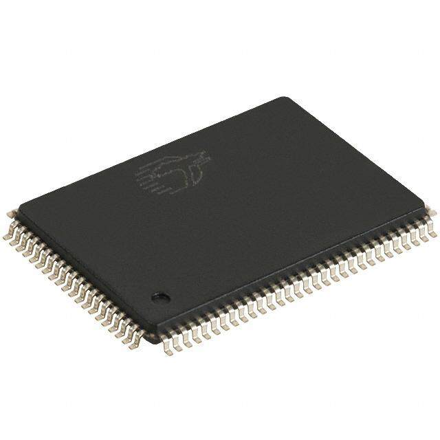
| 产品图片 |
|
| rohs | 符合RoHS无铅 / 符合限制有害物质指令(RoHS)规范要求 |
| 产品系列 | 内存,静态随机存取存储器,Cypress Semiconductor CY7C024E-55AXC- |
| 数据手册 | http://www.cypress.com/?docID=50191 |
| 产品型号 | CY7C024E-55AXC |
| 产品种类 | 静态随机存取存储器 |
| 供应商器件封装 | 100-TQFP(14x14) |
| 其它名称 | 428-3070 |
| 包装 | 托盘 |
| 商标 | Cypress Semiconductor |
| 存储器类型 | SRAM - 双端口,异步 |
| 存储容量 | 64 kbit |
| 存储类型 | SDR |
| 安装风格 | SMD/SMT |
| 封装 | Tray |
| 封装/外壳 | 100-LQFP |
| 封装/箱体 | TQFP-100 |
| 工作温度 | 0°C ~ 70°C |
| 工厂包装数量 | 90 |
| 接口 | Parallel |
| 最大工作温度 | + 70 C |
| 最大工作电流 | 230 mA |
| 最小工作温度 | 0 C |
| 标准包装 | 90 |
| 格式-存储器 | RAM |
| 电压-电源 | 4.5 V ~ 5.5 V |
| 电源电压-最大 | 5.5 V |
| 电源电压-最小 | 4.5 V |
| 类型 | Asynchronous |
| 系列 | CY7C024E |
| 组织 | 4 k x 16 |
| 访问时间 | 55 ns |
| 速度 | 55ns |


_renders/IS45S16320F-7BLA1.jpg)


- 商务部:美国ITC正式对集成电路等产品启动337调查
- 曝三星4nm工艺存在良率问题 高通将骁龙8 Gen1或转产台积电
- 太阳诱电将投资9.5亿元在常州建新厂生产MLCC 预计2023年完工
- 英特尔发布欧洲新工厂建设计划 深化IDM 2.0 战略
- 台积电先进制程称霸业界 有大客户加持明年业绩稳了
- 达到5530亿美元!SIA预计今年全球半导体销售额将创下新高
- 英特尔拟将自动驾驶子公司Mobileye上市 估值或超500亿美元
- 三星加码芯片和SET,合并消费电子和移动部门,撤换高东真等 CEO
- 三星电子宣布重大人事变动 还合并消费电子和移动部门
- 海关总署:前11个月进口集成电路产品价值2.52万亿元 增长14.8%


PDF Datasheet 数据手册内容提取
CY7C024E CY7C025E CY7C0251E 4K × 16 and 8K × 16/18 Dual-Port Static RAM with SEM, INT, BUSY 4K × 16 and 8K × 16/18 Dual-Port Static RAM with SEM, INT, BUSY Features Functional Description ■True dual-ported memory cells that allow simultaneous reads The CY7C024E and CY7C025E/CY7C0251E are low-power of the same memory location CMOS 4K × 16 and 8K × 16/18 dual-port static RAMs. Various arbitration schemes are included on the CY7C024E and ■4K × 16 organization (CY7C024E) CY7C025E/CY7C0251E to handle situations when multiple ■8K × 16 organization (CY7C025E) processors access the same piece of data. Two ports are provided, permitting independent, asynchronous access for ■8K × 18 organization (CY7C0251E) reads and writes to any location in memory. The CY7C024E and CY7C025E/CY7C0251E can be used as standalone 16 or 18-bit ■0.35-µ complementary metal oxide semiconductor (CMOS) for dual-port static RAMs or multiple devices can be combined to optimum speed and power function as a 32-/36-bit or wider master/ slave dual-port static ■High-speed access: 15 ns RAM. An M/S pin is provided for implementing 32-/36-bit or wider memory applications without the need for separate master and ■Low operating power: I = 180 mA (typ), I = 0.05 mA (typ) CC SB3 slave devices or additional discrete logic. Application areas ■Fully asynchronous operation include interprocessor/multiprocessor designs, communications status buffering, and dual-port video/graphics memory. ■Automatic power-down Each port has independent control pins: Chip Enable (CE), Read ■Expandable data bus to 32/36 bits or more using master/slave or Write Enable (R/W), and Output Enable (OE). Two flags are chip select when using more than one device provided on each port (BUSY and INT). BUSY signals that the port is trying to access the same location currently being ■On-chip arbitration logic accessed by the other port. The Interrupt Flag (INT) permits ■Semaphores included to permit software handshaking communication between ports or systems by means of a mail between ports box. The semaphores are used to pass a flag, or token, from one port to the other to indicate that a shared resource is in use. The ■INT flag for port-to-port communication semaphore logic is comprised of eight shared latches. Only one side can control the latch (semaphore) at any time. Control of a ■Separate upper-byte and lower-byte control semaphore indicates that a shared resource is in use. An ■Pin select for master or slave automatic power-down feature is controlled independently on each port by a CE pin. ■Available in Pb-free 100-pin thin quad flatpack (TQFP) package The CY7C024E and CY7C025E/CY7C0251E are available in 100-pin Pb-free TQFP. For a complete list of related documentation, click here. Selection Guide Parameter -15 -25 -55 Maximum access time (ns) 15 25 55 Typical operating current (mA) 190 170 150 Typical standby current for I (mA) 50 40 20 SB1 CypressSemiconductorCorporation • 198 Champion Court • SanJose, CA 95134-1709 • 408-943-2600 Document Number: 001-62932 Rev. *H Revised August 17, 2017
CY7C024E CY7C025E CY7C0251E Logic Block Diagram RU/BWLL RU/BWRR CELLBL LBCRE OEL OERR I/O8L–I/O15[L10] I/O I/O I/O8R–I/O15R[3] I/O0L–I/O7L[9] CONTROL CONTROL I/O0R–I/O7R[2] [6] [1] BUSYL BUSYR (CY7C025E/0251E)A12L A12R(CY7C025E/0251E) A11L ADDEDCROEDSESR MAERMROARYY ADDEDCROEDSESR A11R A0L A0R INTERRUPT CEL SEMAPHORE CER OEL ARBITRATION OER UBL UBR LBL LBR R/WL R/WR SEML SEMR INTL M/S INTR Notes 1. BUSY is an output in master mode and an input in slave mode. 2. I/O0–I/O8 on the CY7C0251E. 3. I/O9–I/O17 on the CY7C0251E. Document Number: 001-62932 Rev. *H Page 2 of 24
CY7C024E CY7C025E CY7C0251E Contents Pin Configurations ...........................................................4 Switching Characteristics ..............................................11 Pin Definitions ..................................................................5 Switching Waveforms ....................................................13 Architecture ......................................................................6 Ordering Information ......................................................19 Functional Overview ........................................................6 4K × 16 Dual-Port SRAM ..........................................19 Write Operation ...........................................................6 8K × 16 Dual-Port SRAM ..........................................19 Read Operation ...........................................................7 Ordering Code Definitions .........................................19 Interrupts .....................................................................7 Package Diagrams ..........................................................20 Busy ............................................................................8 Acronyms ........................................................................21 Master/Slave ...............................................................8 Document Conventions .................................................21 Semaphore Operation .................................................8 Units of Measure .......................................................21 Maximum Ratings .............................................................9 Document History Page .................................................22 Operating Range ...............................................................9 Sales, Solutions, and Legal Information ......................24 Electrical Characteristics .................................................9 Worldwide Sales and Design Support .......................24 Capacitance ....................................................................10 Products ....................................................................24 AC Test Loads and Waveforms .....................................10 PSoC® Solutions ......................................................24 Data Retention Mode ......................................................10 Cypress Developer Community .................................24 Data Retention Timing ...................................................10 Technical Support .....................................................24 Document Number: 001-62932 Rev. *H Page 3 of 24
CY7C024E CY7C025E CY7C0251E Pin Configurations Figure 1. 100-pin TQFP pinout (Top View) I/O9LI/O8LI/O7LI/O6LI/O5LI/O4LI/O3LI/O2LGND I/O1LI/O0LOELVCCR/WLSEMLCELUBLLBLNC[4]A11LA10LA9LA8LA7LA6L 100 999897969594939291908988878685848382818079 787776 75 NC NC 1 74 NC NC 2 73 NC NC 3 72 NC NC 4 71 A5L I/O10L 5 70 A4L III///OOO111123LLL 876 666789 AAA213LLL GND 9 66 A0L I/O14L 10 65 INTL I/O15L 11 CY7C024E/CY7C025E 64 BUSYL VCC 12 63 GND GND 13 62 M/S I/O0R 14 61 BUSYR I/O1R 15 60 INTR I/O2R 16 59 A0R VCC 17 58 A1R I/O3R 18 57 A2R I/O4R 19 56 A3R I/O5R 20 55 A4R I/O6R 21 54 NC NC 22 53 NC NC 23 52 NC NC 24 51 NC NC 25 262728293031323334353637383940414243444546 47484950 I/O7RI/O8RI/O9RI/O10RI/O11RI/O12RI/O13RI/O14RGNDI/O15RŒRR/WRGNDSEMRCERUBRLBRNC[5]A11RA10RA9RA8RA7RA6RA5R Notes 4. A12L on the CY7C025E/CY7C0251E. 5. A12R on the CY7C025E/CY7C0251E. Document Number: 001-62932 Rev. *H Page 4 of 24
CY7C024E CY7C025E CY7C0251E Figure 2. 100-pin TQFP pinout (Top View) 100-Pin TQFP Top View I/O10LI/O9LI/O7LI/O6LI/O5LI/O4LI/O3LI/O2LGND I/O1LI/O0LOELVCCR/WLSEMLCELUBLLBL[6]NCA11LA10LA9LA8LA7LA6L 100 999897969594939291908988878685848382818079787776 75 NC NC 1 74 NC NC 2 73 NC I/O8L 3 72 NC I/O17L 4 71 A5L I/O11L 5 70 A4L III///OOO111234LLL 876 666789 AAA213LLL GND 9 66 A0L I/O15L 10 65 INTL I/O16L 11 CY7C0251E 64 BUSYL VCC 12 63 GND GND 13 62 M/S I/O0R 14 61 BUSYR I/O1R 15 60 INTR I/O2R 16 59 A0R VCC 17 58 A1R I/O3R 18 57 A2R I/O4R 19 56 A3R I/O5R 20 55 A4R I/O6R 21 54 NC I/O8R 22 53 NC I/O17R 23 52 NC NC 24 51 NC NC 25 262728293031323334353637383940414243444546 47484950 I/O7RI/O9RI/O10RI/O11RI/O12RI/O13RI/O14RI/O15RGNDI/O16ROE RR/WRGNDSEMRCERUBRLBR[7]NCA11RA10RA9RA8RA7RA6RA5R Pin Definitions Left Port Right Port Description CE CE Chip enable L R R/W R/W Read/write enable L R OE OE Output enable L R A –A A –A Address 0L 11/12L 0R 11/12R I/O –I/O I/O –I/O Data bus input/output 0L 15/17L 0R 15/17R SEM SEM Semaphore enable L R UB UB Upper byte select L R LB LB Lower byte select L R INT INT Interrupt flag L R BUSY [8] BUSY [8] Busy flag L R M/S Master or slave select V Power CC GND Ground Notes 6. A12L on the CY7C025E/CY7C0251E. 7. A12R on the CY7C025E/CY7C0251E. 8. BUSY is an output in master mode and an input in slave mode. Document Number: 001-62932 Rev. *H Page 5 of 24
CY7C024E CY7C025E CY7C0251E Architecture Functional Overview The CY7C024E and CY7C025E/CY7C0251E consist of an array Write Operation of 4K words of 16 bits each and 8K words of 16/18 bits each of dual-port RAM cells, I/O and address lines, and control signals Data must be set up for a duration of tSD before the rising edge (CE, OE, R/W). These control pins permit independent access of R/W to guarantee a valid write. A write operation is controlled for reads or writes to any location in memory. To handle by either the R/W pin (see Figure7) or the CE pin (see Figure8). simultaneous writes/reads to the same location, a BUSY pin is Required inputs for non-contention operations are summarized provided on each port. Two interrupt (INT) pins can be used for in Table1. port-to-port communication. Two semaphore (SEM) control pins If a location is being written to by one port and the opposite port are used for allocating shared resources. With the M/S pin, the attempts to read that location, a port-to-port flowthrough delay CY7C024E and CY7C025E/CY7C0251E can function as a must occur before the data is read on the output; otherwise the master (BUSY pins are outputs) or as a slave (BUSY pins are data read is not deterministic. Data is valid on the port t after DDD inputs). The CY7C024E and CY7C025E/CY7C0251E have an the data is presented on the other port. automatic power-down feature controlled by CE. Each port is provided with its own output enable control (OE), which allows data to be read from the device. Table 1. Non-Contending Read/Write Inputs Outputs Operation CE R/W OE UB LB SEM I/O –I/O [9] I/O –I/O [10] 0 7 8 15 H X X X X H High Z High Z Deselected: power-down X X X H H H High Z High Z Deselected: power-down L L X L H H High Z Data in Write to upper byte only L L X H L H Data in High Z Write to lower byte only L L X L L H Data in Data in Write to both bytes L H L L H H High Z Data out Read upper byte only L H L H L H Data out High Z Read lower byte only L H L L L H Data out Data out Read both bytes X X H X X X High Z High Z Outputs disabled H H L X X L Data out Data out Read data in semaphore flag X H L H H L Data out Data out Read data in semaphore flag H X X X L Data in Data in Write D into semaphore flag IN0 X X H H L Data in Data in Write D into semaphore flag IN0 L X X L X L Not allowed L X X X L L Not allowed Notes 9. I/O0–I/O8 on the CY7C0251E. 10.I/O9–I/O17 on the CY7C0251E. Document Number: 001-62932 Rev. *H Page 6 of 24
CY7C024E CY7C025E CY7C0251E Read Operation mailbox, an interrupt is generated to the owner. The interrupt is reset when the owner reads the contents of the mailbox. The When reading the device, the user must assert both the OE and message is user-defined. CE pins. Data is available t after CE or t after OE is ACE DOE asserted. If the user of the CY7C024E and Each port can read the other port’s mailbox without resetting the CY7C025E/CY7C0251E wishes to access a semaphore flag, interrupt. The active state of the BUSY signal (to a port) prevents then the SEM pin must be asserted instead of the CE pin, and the port from setting the interrupt to the winning port. Also, an OE must also be asserted. active BUSY to a port prevents that port from reading its own mailbox and thus resetting the interrupt to it. Interrupts If your application does not require message passing, do not The upper two memory locations may be used for message connect the interrupt pin to the processor’s interrupt request passing. The highest memory location (FFF for the CY7C024E, input pin. 1FFF for the CY7C025E/CY7C0251E) is the mailbox for the right The operation of the interrupts and their interaction with Busy are port and the second-highest memory location (FFE for the summarized in Table2. CY7C024E, 1FFE for the CY7C025E/CY7C0251E) is the mailbox for the left port. When one port writes to the other port’s Table 2. Interrupt Operation Example (Assumes BUSY =BUSY =HIGH)[11] L R Left Port Right Port Function R/W CE OE A INT R/W CE OE A INT L L L 0L–11L L R R R 0R–11R R Set right INT flag L L X (1)FFF X X X X X L[12] R Reset right INT flag X X X X X X L L (1)FFF H[13] R Set left INT flag X X X X L[13] L L X (1)FFE X L Reset left INT flag X L L (1)FFE H[12] X X X X X L Notes 11.A0L–12L and A0R–12R, 1FFF/1FFE for the CY7C025E/CY7C0251E. 12.If BUSYL = L, then no change. 13.If BUSYR = L, then no change. Document Number: 001-62932 Rev. *H Page 7 of 24
CY7C024E CY7C025E CY7C0251E Busy available t + t after the rising edge of the semaphore SWRD DOE write. If the left port was successful (reads a zero), it assumes The CY7C024E and CY7C025E/CY7C0251E provide on-chip control of the shared resource, otherwise (reads a one) it arbitration to resolve simultaneous memory location access assumes the right port has control and continues to poll the (contention). If both ports’ CEs are asserted and an address semaphore. When the right side has relinquished control of the match occurs within tPS of each other, the busy logic determines semaphore (by writing a one), the left side succeeds in gaining which port has access. If tPS is violated, one port definitely gains control of the semaphore. If the left side no longer requires the permission to the location, but which one is not predictable. semaphore, a one is written to cancel its request. BUSY is asserted t after an address match or t after CE BLA BLC is taken LOW. Semaphores are accessed by asserting SEM LOW. The SEM pin functions as a chip select for the semaphore latches (CE Master/Slave must remain HIGH during SEM LOW). A represents the 0–2 semaphore address. OE and R/W are used in the same manner A M/S pin is provided to expand the word width by configuring as a normal memory access. When writing or reading a the device as either a master or a slave. The BUSY output of the semaphore, the other address pins have no effect. master is connected to the BUSY input of the slave. This allows the device to interface to a master device with no external When writing to the semaphore, only I/O is used. If a zero is 0 components. Writing to slave devices must be delayed until after written to the left port of an available semaphore, a one appears the BUSY input has settled (t or t ). Otherwise, the slave at the same semaphore address on the right port. That BLC BLA chip may begin a write cycle during a contention situation. When semaphore can now only be modified by the side showing zero tied HIGH, the M/S pin allows the device to be used as a master (the left port in this case). If the left port now relinquishes control and, therefore, the BUSY line is an output. BUSY can then be by writing a one to the semaphore, the semaphore is set to one used to send the arbitration outcome to a slave. for both sides. However, if the right port had requested the semaphore (written a zero) while the left port had control, the Semaphore Operation right port immediately owns the semaphore as soon as the left The CY7C024E and CY7C025E/CY7C0251E provide eight port releases it. Table3 shows sample semaphore operations. semaphore latches, which are separate from the dual-port When reading a semaphore, all 16/18 data lines output the memory locations. Semaphores are used to reserve resources semaphore value. The read value is latched in an output register that are shared between the two ports. The state of the to prevent the semaphore from changing state during a write semaphore indicates that a resource is in use. For example, if from the other port. If both ports attempt to access the the left port wants to request a given resource, it sets a latch by semaphore within t of each other, the semaphore is definitely SPS writing a zero to a semaphore location. The left port then verifies obtained by one side or the other, but there is no guarantee which its success in setting the latch by reading it. After writing to the side controls the semaphore. semaphore, SEM or OE must be deasserted for t before SOP attempting to read the semaphore. The semaphore value is Table 3. Semaphore Operation Example I/O –I/O I/O –I/O Function 0 15/17 0 15/17 Status Left Right No action 1 1 Semaphore-free Left port writes 0 to semaphore 0 1 Left port has semaphore token Right port writes 0 to semaphore 0 1 No change. Right side has no write access to semaphore. Left port writes 1 to semaphore 1 0 Right port obtains semaphore token Left port writes 0 to semaphore 1 0 No change. Left port has no write access to semaphore Right port writes 1 to semaphore 0 1 Left port obtains semaphore token Left port writes 1 to semaphore 1 1 Semaphore-free Right port writes 0 to semaphore 1 0 Right port has semaphore token Right port writes 1 to semaphore 1 1 Semaphore-free Left port writes 0 to semaphore 0 1 Left port has semaphore token Left port writes 1 to semaphore 1 1 Semaphore-free Document Number: 001-62932 Rev. *H Page 8 of 24
CY7C024E CY7C025E CY7C0251E Maximum Ratings DC input voltage[15] .....................................–0.5 V to +7.0 V Output current into outputs (LOW) .............................20 mA Exceeding maximum ratings[14] may shorten the useful life of the Static discharge voltage device. User guidelines are not tested. (per MIL-STD-883, Method 3015) ......................... > 2001 V Storage temperature ................................–65 °C to +150 °C Latch-up current ................................................... > 200 mA Ambient temperature with power applied ...................................–55 °C to +125 °C Operating Range Supply voltage to ground potential ..............–0.3 V to +7.0 V Range Ambient Temperature V CC DC voltage applied to outputs Commercial 0 °C to +70 °C 5 V 10% in high Z state...............................................–0.5 V to +7.0 V Industrial –40 °C to +85 °C 5 V 10% Electrical Characteristics Over the Operating Range -15 -25 -55 Parameter Description Test Conditions Unit Min Typ Max Min Typ Max Min Typ Max V Output HIGH V = Min, I = –4.0 mA 2.4 – – 2.4 – – 2.4 – – V OH CC OH voltage V Output LOW V = Min, I = 4.0 mA – – 0.4 – – 0.4 – – 0.4 V OL CC OL voltage V Input HIGH voltage 2.2 – – 2.2 – – 2.2 – – V IH V Input LOW voltage – – 0.8 – – 0.8 – – 0.8 V IL I Input leakage GND V V –10 – +10 –10 – +10 –10 – +10 A IX I CC current I Output leakage Output disabled, –10 – +10 –10 – +10 –10 – +10 A OZ current GND V V O CC I Operating current V = Max, I = 0 mA, Commercial – 190 285 – 170 250 – 150 230 mA CC CC OUT Outputs Disabled Industrial – 215 305 – 180 290 – 180 290 I Standby current CE and CE V , Commercial – 50 70 – 40 60 – 20 50 mA SB1 L R IH (both ports TTL f = f [16] MAX Industrial – 65 95 – 55 80 – 55 80 levels) I Standby current CE or CE V , Commercial – 120 180 – 100 150 – 75 135 mA SB2 L R IH (one port TTL level) f = f [16] MAX Industrial – 135 205 – 120 175 – 120 175 I Standby current Both Ports CE and CE Commercial – 0.05 0.5 – 0.05 0.50 – 0.05 0.50 mA SB3 R (both ports CMOS V – 0.2 V, V V – 0.2 V levels) orC VC 0.2 V, IfN = 0[1C6C] Industrial – 0.05 0.5 – 0.05 0.50 – 0.05 0.50 IN I Standby current One Port CE or Commercial – 110 160 – 90 130 – 70 120 mA SB4 L (both ports CMOS CE V – 0.2 V, R CC Industrial – 125 175 – 110 150 – 110 150 levels) V V – 0.2 V or V 0.2 V, IN CC IN Active Port Outputs, f = f [16] MAX Notes 14.The voltage on any input or I/O pin cannot exceed the power pin during power-up. 15.Pulse width < 20 ns. 16.fMAX = 1/tRC = All inputs cycling at f = 1/tRC (except output enable). f = 0 means no address or control lines change. This applies only to inputs at CMOS level standby ISB3. Document Number: 001-62932 Rev. *H Page 9 of 24
CY7C024E CY7C025E CY7C0251E Capacitance Parameter [17] Description Test Conditions Max Unit C Input capacitance T = 25 °C, f = 1 MHz, 10 pF IN A V = 5.0 V C Output capacitance CC 10 pF OUT AC Test Loads and Waveforms Figure 3. AC Test Loads and Waveforms 5 V 5 V R1= 893 RTH= 250 OUTPUT R1= 893 OUTPUT OUTPUT C= 30 pF C= 30pF R2= 347 C= 5pF R2= 347 VTH= 1.4 V (a)Normal Load(Load 1) (b) ThéveninEquivalent (Load1) (c)Three-State Delay(Load3) ALLINPUTPULSES OUTPUT 3.0 V 90% 10% 90% 10% C= 30pF GND 3ns 3ns Load (Load2) Data Retention Mode Data Retention Timing The CY7C024E is designed with battery backup in mind. Data retention voltage and supply current are guaranteed over Data Retention Mode temperature. The following rules insure data retention: 1.Chip enable (CE) must be held HIGH during data retention, VCC 4.5 V 4.5 V within VCC to VCC – 0.2 V. VCC2.0 V tRC 2.CE must be kept between V – 0.2 V and 70% of V during CC CC the power up and power down transitions. VCCtoVCC– 0.2 V V CE IH 3.The RAM can begin operation >t after V reaches the RC CC minimum operating voltage (4.5 V). Parameter Test Conditions[18] Max Unit ICC At VCC = 2 V 1.5 mA DR1 DR Notes 17.Tested initially and after any design or process changes that may affect these parameters. 18.CE = VCC, Vin = GND to VCC, TA = 25C. This parameter is guaranteed but not tested. Document Number: 001-62932 Rev. *H Page 10 of 24
CY7C024E CY7C025E CY7C0251E Switching Characteristics Over the Operating Range -15 -25 -55 Parameter [19] Description Unit Min Max Min Max Min Max Read Cycle t Read cycle time 15 – 25 – 55 – ns RC t Address to data valid – 15 – 25 – 55 ns AA t Output hold from address change 3 – 3 – 3 – ns OHA t [20] CE LOW to data valid – 15 – 25 – 55 ns ACE t OE LOW to data valid – 10 – 13 – 25 ns DOE t [21, 22, 23] OE low to low Z 3 – 3 – 3 – ns LZOE t [21,22, 23] OE HIGH to high Z – 10 – 15 – 25 ns HZOE t [21, 22, 23] CE LOW to low Z 3 – 3 – 3 – ns LZCE t [21, 22, 23] CE HIGH to High Z – 10 – 15 – 25 ns HZCE t [23] CE LOW to power-up 0 – 0 – 0 – ns PU t [23] CE HIGH to power-down – 15 – 25 – 55 ns PD t [20] Byte enable access time – 15 – 25 – 55 ns ABE Write Cycle t Write cycle time 15 – 25 – 55 – ns WC t [20] CE LOW to write end 12 – 20 – 35 – ns SCE t Address setup to write end 12 – 20 – 35 – ns AW t Address hold from write end 0 – 0 – 0 – ns HA t [24] Address setup to write start 0 – 0 – 0 – ns SA t Write pulse width 12 – 20 – 35 – ns PWE t Data setup to write end 10 – 15 – 20 – ns SD t Data hold from write end 0 – 0 – 0 – ns HD t [25, 26] R/W LOW to high Z – 10 – 15 – 25 ns HZWE t [25, 26] R/W HIGH to low Z 3 – 3 – 3 – ns LZWE t [27] Write pulse to data delay – 30 – 50 – 70 ns WDD t [27] Write data valid to read – 25 – 35 – 45 ns DDD data valid Notes 19.Test conditions assume signal transition time of 3 ns or less, timing reference levels of 1.5 V, input pulse levels of 0 to 3.0 V, and output loading of the specified IOI/IOH and 30 pF load capacitance. 20.To access RAM, CE=L, UB=L, SEM=H. To access semaphore, CE=H and SEM=L. Either condition must be valid for the entire tSCE time. 21.At any given temperature and voltage condition for any given device, tHZCE is less than tLZCE and tHZOE is less than tLZOE. 22.Test conditions used are Load 3. 23.This parameter is guaranteed but not tested. 24.To access RAM, CE=L, UB=L, SEM=H. To access semaphore, CE=H and SEM=L. Either condition must be valid for the entire tSCE time. 25.Test conditions used are Load 3. 26.This parameter is guaranteed but not tested. 27.For information on port-to-port delay through RAM cells from writing port to reading port, refer to Figure 11 on page 16. Document Number: 001-62932 Rev. *H Page 11 of 24
CY7C024E CY7C025E CY7C0251E Switching Characteristics (continued) Over the Operating Range -15 -25 -55 Parameter [19] Description Unit Min Max Min Max Min Max Busy Timing[28] t BUSY LOW from Address Match – 15 – 20 – 45 ns BLA t BUSY HIGH from Address – 15 – 20 – 40 ns BHA Mismatch t BUSY LOW from CE LOW – 15 – 20 – 40 ns BLC t BUSY HIGH from CE HIGH – 15 – 20 – 35 ns BHC t Port Setup for Priority 5 – 5 – 5 – ns PS t R/W HIGH after BUSY (Slave) 0 – 0 – 0 – ns WB t R/W HIGH after BUSY HIGH (Slave) 13 – 20 – 40 – ns WH t [29] BUSY HIGH to Data Valid – Note 29 Note 29 Note 29 ns BDD Interrupt Timing[28] t INT Set Time – 15 – 20 – 30 ns INS t INT Reset Time – 15 – 20 – 30 ns INR Semaphore Timing t SEM Flag Update Pulse (OE or SEM) 10 – 12 – 20 – ns SOP t SEM Flag Write to Read Time 5 – 10 – 15 – ns SWRD t SEM Flag Contention Window 5 – 10 – 15 – ns SPS t SEM Address Access Time – 15 25 – 55 ns SAA Notes 28.Test conditions used are Load 2. 29.tBDD is a calculated parameter and is the greater of tWDD– tPWE (actual) or tDDD– tSD (actual). Document Number: 001-62932 Rev. *H Page 12 of 24
CY7C024E CY7C025E CY7C0251E Switching Waveforms Figure 4. Read Cycle No. 1 (Either Port Address Access) [30, 31, 32] tRC ADDRESS tAA tOHA tOHA DATA OUT PREVIOUS DATA VALID DATA VALID Figure 5. Read Cycle No. 2 (Either Port CE/OE Access) [30, 33, 34] tACE CEand LBorUB tHZCE tDOE OE tHZOE tLZOE DATA OUT DATA VALID tLZCE tPU tPD ICC CURRENT ISB Figure 6. Read Cycle No. 3 (Either Port) [30, 32, 33, 34] tRC ADDRESS tAA tOHA UBorLB tHZCE tLZCE tABE CE tHZCE tACE tLZCE DATAOUT Notes 30.R/W is HIGH for read cycles. 31.Device is continuously selected CE = VIL and UB or LB = VIL. This waveform cannot be used for semaphore reads. 32.OE = VIL. 33.Address valid prior to or coincident with CE transition LOW. 34.To access RAM, CE = VIL, UB or LB = VIL, SEM = VIH. To access semaphore, CE = VIH, SEM = VIL. Document Number: 001-62932 Rev. *H Page 13 of 24
CY7C024E CY7C025E CY7C0251E Switching Waveforms (continued) Figure 7. Write Cycle No. 1 (R/W Controlled Timing) [35,36,37,38] tWC ADDRESS tHZOE[41] OE tAW [39,40] CE tSA tPWE[38] tHA R/W tHZWE[41] tLZWE DATAOUT NOTE 42 NOTE 42 tSD tHD DATA IN Figure 8. Write Cycle No. 2 (CE Controlled Timing) [35,36,37,43] tWC ADDRESS tAW [39,40] CE tSA tSCE tHA R/W tSD tHD DATA IN Notes 35.R/W must be HIGH during all address transitions. 36.A write occurs during the overlap (tSCE or tPWE) of a LOW CE or SEM and a LOW UB or LB. 37.tHA is measured from the earlier of CE or R/W or (SEM or R/W) going HIGH at the end of write cycle. 38.If OE is LOW during a R/W controlled write cycle, the write pulse width must be the larger of tPWE or (tHZWE + tSD) to allow the I/O drivers to turn off and data to be placed on the bus for the required tSD. If OE is HIGH during an R/W controlled write cycle, this requirement does not apply and the write pulse can be as short as the specified tPWE. 39.To access RAM, CE = VIL, SEM = VIH. 40.To access upper byte, CE = VIL, UB = VIL, SEM = VIH. To access lower byte, CE = VIL, LB = VIL, SEM = VIH. 41.Transition is measured ±500 mV from steady state with a 5 pF load (including scope and jig). This parameter is sampled and not 100% tested. 42.During this period, the I/O pins are in the output state, and input signals must not be applied. 43.If the CE or SEM LOW transition occurs simultaneously with or after the R/W LOW transition, the outputs remain in the high impedance state. Document Number: 001-62932 Rev. *H Page 14 of 24
CY7C024E CY7C025E CY7C0251E Switching Waveforms (continued) Figure 9. Semaphore Read After Write Timing, Either Side [44] tAA tOHA A0–A2 VALID ADRESS VALID ADRESS tAW tACE tHA SEM tSCE tSOP tSD I/O0 DATAINVALID DATAOUTVALID tSA tPWE tHD R/W tSWRD tDOE OE tSOP WRITE CYCLE READ CYCLE Figure 10. Timing Diagram of Semaphore Contention [45,46,47] A0L–A2L MATCH R/WL SEML tSPS A0R–A2R MATCH R/WR SEMR Notes 44.CE = HIGH for the duration of the above timing (both write and read cycle). 45.I/O0R = I/O0L = LOW (request semaphore); CER = CEL = HIGH. 46.Semaphores are reset (available to both ports) at cycle start. 47.If tSPS is violated, the semaphore is definitely obtained by one side or the other, but which side gets the semaphore is unpredictable. Document Number: 001-62932 Rev. *H Page 15 of 24
CY7C024E CY7C025E CY7C0251E Switching Waveforms (continued) Figure 11. Timing Diagram of Read with BUSY (M/S = HIGH) [48] tWC ADDRESSR MATCH R/WR tPWE tSD tHD DATA INR VALID tPS ADDRESSL MATCH tBLA tBHA BUSYL tBDD tDDD DATAOUTL VALID tWDD Figure 12. Write Timing with Busy Input (M/S = LOW) tPWE R/W tWB tWH BUSY Note 48.CEL = CER = LOW. Document Number: 001-62932 Rev. *H Page 16 of 24
CY7C024E CY7C025E CY7C0251E Switching Waveforms (continued) Figure 13. Busy Timing Diagram No. 1 (CE Arbitration) [49] CE Valid First: L ADDRESSL,R ADDRESS MATCH CEL tPS CER tBLC tBHC BUSYR CE ValidFirst: R ADDRESSL,R ADDRESS MATCH CER tPS CEL tBLC tBHC BUSYL Figure 14. Busy Timing Diagram No. 2 (Address Arbitration) [49] Left Address Valid First: tRCortWC ADDRESSL ADDRESS MATCH ADDRESS MISMATCH tPS ADDRESSR tBLA tBHA BUSYR RightAddressValidFirst: tRCortWC ADDRESSR ADDRESS MATCH ADDRESS MISMATCH tPS ADDRESSL tBLA tBHA BUSYL Note 49.If tPS is violated, the busy signal is asserted on one side or the other, but there is no guarantee to which side BUSY is asserted. Document Number: 001-62932 Rev. *H Page 17 of 24
CY7C024E CY7C025E CY7C0251E Switching Waveforms (continued) Figure 15. Interrupt Timing Diagrams LeftSideSetsINT : R tWC ADDRESSL WRITE FFF (1FFF CY7C025) [50] CEL tHA R/WL INTR tINS[51] RightSideClearsINT : R tRC READ FFF ADDRESSR (1FFF CY7C025) CER tINR[51] R/WR OER INTR RightSideSetsINT : L tWC ADDRESSR WRITE FFE (1FFE CY7C025) tHA[50] CER R/WR INTL [51] tINS Left SideClearsINT : L tRC READ FFE ADDRESSR (1FFE CY7C025) CEL tINR[51] R/WL OEL INTL Notes 50.tHA depends on which enable pin (CEL or R/WL) is deasserted first. 51.tINS or tINR depends on which enable pin (CEL or R/WL) is asserted last. Document Number: 001-62932 Rev. *H Page 18 of 24
CY7C024E CY7C025E CY7C0251E Ordering Information 4K × 16 Dual-Port SRAM Speed Package Operating Ordering Code Package Type (ns) Name Range 15 CY7C024E-15AXC A100 100-pin TQFP (Pb-free) Commercial 25 CY7C024E-25AXC A100 100-pin TQFP (Pb-free) Commercial CY7C024E-25AXI A100 100-pin TQFP (Pb-free) Industrial 55 CY7C024E-55AXC A100 100-pin TQFP (Pb-free) Commercial 8K × 16 Dual-Port SRAM Speed Package Operating Ordering Code Package Type (ns) Name Range 25 CY7C025E-25AXC A100 100-pin TQFP (Pb-free) Commercial CY7C025E-25AXI A100 100-pin TQFP (Pb-free) Industrial Ordering Code Definitions CY 7 C 02X X E - XX A X X Temperature Range: X = C or I C = Commercial; I = Industrial Pb-free Package Type: A = 100-pin TQFP Speed: XX = 15 ns or 25 ns or 55 ns Die Revision Data width: X = blank or 1 blank = × 16; 1 = × 18 Density: 02X = 024 or 025 024 = 4-Kbit; 025 = 8-Kbit Technology Code: C = CMOS Marketing Code: 7 = SRAM Company ID: CY = Cypress Document Number: 001-62932 Rev. *H Page 19 of 24
CY7C024E CY7C025E CY7C0251E Package Diagrams Figure 16. 100-pin TQFP (14 × 14 × 1.4 mm) A100SA Package Outline, 51-85048 51-85048 *J Document Number: 001-62932 Rev. *H Page 20 of 24
CY7C024E CY7C025E CY7C0251E Acronyms Document Conventions Units of Measure Acronym Description CE Chip Enable Symbol Unit of Measure CMOS Complementary Metal Oxide Semiconductor °C degree Celsius I/O Input/Output MHz megahertz OE Output Enable A microampere SRAM Static Random Access Memory mA milliampere ns nanosecond TQFP Thin Quad Flat Pack ohm % percent pF picofarad V volt W watt Document Number: 001-62932 Rev. *H Page 21 of 24
CY7C024E CY7C025E CY7C0251E Document History Page Document Title: CY7C024E/CY7C025E/CY7C0251E, 4K × 16 and 8K × 16/18 Dual-Port Static RAM with SEM, INT, BUSY Document Number: 001-62932 Orig. of Submission Rev. ECN No. Description of Change Change Date ** 2975554 RAME 07/09/2010 New data sheet. *A 3056347 ADMU 10/28/2010 Updated Selection Guide: Changed Typical Operating current (mA) from 180 mA to 170 mA (corresponding to speed bin -25). Changed Typical standby current for I (mA) from 45 mA to 40 mA SB1 (corresponding to speed bin -25). Changed Typical Operating current (mA) from 180 mA to 150 mA (corresponding to speed bin -55). Changed Typical standby current for I (mA) from 45 mA to 20 mA SB1 (corresponding to speed bin -55). Updated Electrical Characteristics: Separated values corresponding to speed bins -25 and -55 into two separate columns. Changed typical value of I parameter from 180 mA to 170 mA CC (corresponding to speed bin -25 and test condition “Commercial”). Changed maximum value of I parameter from 275 mA to 250 mA CC (corresponding to speed bin -25 and test condition “Commercial”). Changed typical value of I parameter from 180 mA to 150 mA CC (corresponding to speed bin -55 and test condition “Commercial”). Changed maximum value of I parameter from 275 mA to 230 mA CC (corresponding to speed bin -55 and test condition “Commercial”). Changed typical value of I parameter from 45 mA to 40 mA (corresponding SB1 to speed bin -25 and test condition “Commercial”). Changed maximum value of I parameter from 65 mA to 60 mA SB1 (corresponding to speed bin -25 and test condition “Commercial”). Changed typical value of I parameter from 45 mA to 20 mA (corresponding SB1 to speed bin -55 and test condition “Commercial”). Changed maximum value of I parameter from 65 mA to 50 mA SB1 (corresponding to speed bin -55 and test condition “Commercial”). Changed typical value of I parameter from 110 mA to 100 mA SB2 (corresponding to speed bin -25 and test condition “Commercial”). Changed maximum value of I parameter from 160 mA to 150 mA SB2 (corresponding to speed bin -25 and test condition “Commercial”). Changed typical value of I parameter from 110 mA to 75 mA (corresponding SB2 to speed bin -55 and test condition “Commercial”). Changed maximum value of I parameter from 160 mA to 135 mA SB2 (corresponding to speed bin -55 and test condition “Commercial”). Changed typical value of I parameter from 100 mA to 90 mA (corresponding SB4 to speed bin -25 and test condition “Commercial”). Changed maximum value of I parameter from 140 mA to 130 mA SB4 (corresponding to speed bin -25 and test condition “Commercial”). Changed typical value of I parameter from 100 mA to 70 mA (corresponding SB4 to speed bin -55 and test condition “Commercial”). Changed maximum value of I parameter from 140 mA to 120 mA SB4 (corresponding to speed bin -55 and test condition “Commercial”). Updated Ordering Information: Updated part numbers. *B 3247559 ADMU 05/04/2011 Updated Electrical Characteristics: Removed minimum value of V parameter (for all speed bins). IL Updated Ordering Code Definitions under Ordering Information. Updated Package Diagrams: spec 51-85048 – Changed revision from *D to *E. Document Number: 001-62932 Rev. *H Page 22 of 24
CY7C024E CY7C025E CY7C0251E Document History Page (continued) Document Title: CY7C024E/CY7C025E/CY7C0251E, 4K × 16 and 8K × 16/18 Dual-Port Static RAM with SEM, INT, BUSY Document Number: 001-62932 Orig. of Submission Rev. ECN No. Description of Change Change Date *C 3864478 ADMU 01/10/2013 Updated Ordering Information: Updated part numbers. Updated Package Diagrams: spec 51-85048 – Changed revision from *E to *G. *D 4075480 ADMU 07/24/2013 Updated Logic Block Diagram. Updated Pin Configurations. Updated to new template. Completing Sunset Review. *E 4093991 ADMU 08/13/2013 Updated Package Diagrams: spec 51-85048 – Changed revision from *G to *H. Added Units of Measure. *F 4447806 ADMU 07/18/2014 Removed CY7C0241E related information in all instances across the document. Updated Ordering Information: Updated part numbers. Updated Package Diagrams: spec 51-85048 – Changed revision from *H to *I. *G 4580426 ADMU 11/24/2014 Updated Functional Description: Added “For a complete list of related documentation, click here.” at the end. *H 5856565 VINI 08/17/2017 Updated Ordering Information: Updated part numbers. Updated Package Diagrams: spec 51-85048 – Changed revision from *I to *J. Updated to new template. Completing Sunset Review. Document Number: 001-62932 Rev. *H Page 23 of 24
CY7C024E CY7C025E CY7C0251E Sales, Solutions, and Legal Information Worldwide Sales and Design Support Cypress maintains a worldwide network of offices, solution centers, manufacturer’s representatives, and distributors. To find the office closest to you, visit us at Cypress Locations. Products PSoC® Solutions ARM® Cortex® Microcontrollers cypress.com/arm PSoC 1 | PSoC 3 | PSoC 4 | PSoC 5LP Automotive cypress.com/automotive Cypress Developer Community Clocks & Buffers cypress.com/clocks Forums | WICED IOT Forums | Projects | Video | Blogs | Interface cypress.com/interface Training | Components Internet of Things cypress.com/iot Technical Support Memory cypress.com/memory cypress.com/support Microcontrollers cypress.com/mcu PSoC cypress.com/psoc Power Management ICs cypress.com/pmic Touch Sensing cypress.com/touch USB Controllers cypress.com/usb Wireless Connectivity cypress.com/wireless © Cypress Semiconductor Corporation, 2010–2017. This document is the property of Cypress Semiconductor Corporation and its subsidiaries, including Spansion LLC ("Cypress"). This document, including any software or firmware included or referenced in this document ("Software"), is owned by Cypress under the intellectual property laws and treaties of the United States and other countries worldwide. Cypress reserves all rights under such laws and treaties and does not, except as specifically stated in this paragraph, grant any license under its patents, copyrights, trademarks, or other intellectual property rights. If the Software is not accompanied by a license agreement and you do not otherwise have a written agreement with Cypress governing the use of the Software, then Cypress hereby grants you a personal, non-exclusive, nontransferable license (without the right to sublicense) (1) under its copyright rights in the Software (a) for Software provided in source code form, to modify and reproduce the Software solely for use with Cypress hardware products, only internally within your organization, and (b) to distribute the Software in binary code form externally to end users (either directly or indirectly through resellers and distributors), solely for use on Cypress hardware product units, and (2) under those claims of Cypress's patents that are infringed by the Software (as provided by Cypress, unmodified) to make, use, distribute, and import the Software solely for use with Cypress hardware products. Any other use, reproduction, modification, translation, or compilation of the Software is prohibited. TO THE EXTENT PERMITTED BY APPLICABLE LAW, CYPRESS MAKES NO WARRANTY OF ANY KIND, EXPRESS OR IMPLIED, WITH REGARD TO THIS DOCUMENT OR ANY SOFTWARE OR ACCOMPANYING HARDWARE, INCLUDING, BUT NOT LIMITED TO, THE IMPLIED WARRANTIES OF MERCHANTABILITY AND FITNESS FOR A PARTICULAR PURPOSE. To the extent permitted by applicable law, Cypress reserves the right to make changes to this document without further notice. Cypress does not assume any liability arising out of the application or use of any product or circuit described in this document. Any information provided in this document, including any sample design information or programming code, is provided only for reference purposes. It is the responsibility of the user of this document to properly design, program, and test the functionality and safety of any application made of this information and any resulting product. Cypress products are not designed, intended, or authorized for use as critical components in systems designed or intended for the operation of weapons, weapons systems, nuclear installations, life-support devices or systems, other medical devices or systems (including resuscitation equipment and surgical implants), pollution control or hazardous substances management, or other uses where the failure of the device or system could cause personal injury, death, or property damage ("Unintended Uses"). A critical component is any component of a device or system whose failure to perform can be reasonably expected to cause the failure of the device or system, or to affect its safety or effectiveness. Cypress is not liable, in whole or in part, and you shall and hereby do release Cypress from any claim, damage, or other liability arising from or related to all Unintended Uses of Cypress products. You shall indemnify and hold Cypress harmless from and against all claims, costs, damages, and other liabilities, including claims for personal injury or death, arising from or related to any Unintended Uses of Cypress products. Cypress, the Cypress logo, Spansion, the Spansion logo, and combinations thereof, WICED, PSoC, CapSense, EZ-USB, F-RAM, and Traveo are trademarks or registered trademarks of Cypress in the United States and other countries. For a more complete list of Cypress trademarks, visit cypress.com. Other names and brands may be claimed as property of their respective owners. Document Number: 001-62932 Rev. *H Revised August 17, 2017 Page 24 of 24