ICGOO在线商城 > 集成电路(IC) > 逻辑 - 缓冲器,驱动器,接收器,收发器 > CY74FCT2541CTQCT

 Datasheet下载
- 型号: CY74FCT2541CTQCT
- 制造商: Texas Instruments
- 库位|库存: xxxx|xxxx
- 要求:
| 数量阶梯 | 香港交货 | 国内含税 |
| +xxxx | $xxxx | ¥xxxx |
查看当月历史价格
查看今年历史价格
CY74FCT2541CTQCT产品简介:
ICGOO电子元器件商城为您提供CY74FCT2541CTQCT由Texas Instruments设计生产,在icgoo商城现货销售,并且可以通过原厂、代理商等渠道进行代购。 CY74FCT2541CTQCT价格参考。Texas InstrumentsCY74FCT2541CTQCT封装/规格:逻辑 - 缓冲器,驱动器,接收器,收发器, Buffer, Non-Inverting 1 Element 8 Bit per Element 3-State Output 20-SSOP/QSOP。您可以下载CY74FCT2541CTQCT参考资料、Datasheet数据手册功能说明书,资料中有CY74FCT2541CTQCT 详细功能的应用电路图电压和使用方法及教程。
| 参数 | 数值 |
| 产品目录 | 集成电路 (IC)半导体 |
| 描述 | IC BUFF/DVR TRI-ST 8BIT 20QSOP缓冲器和线路驱动器 Octal Line/MOS Drv w/3-State Output |
| 产品分类 | |
| 品牌 | Texas Instruments |
| 产品手册 | |
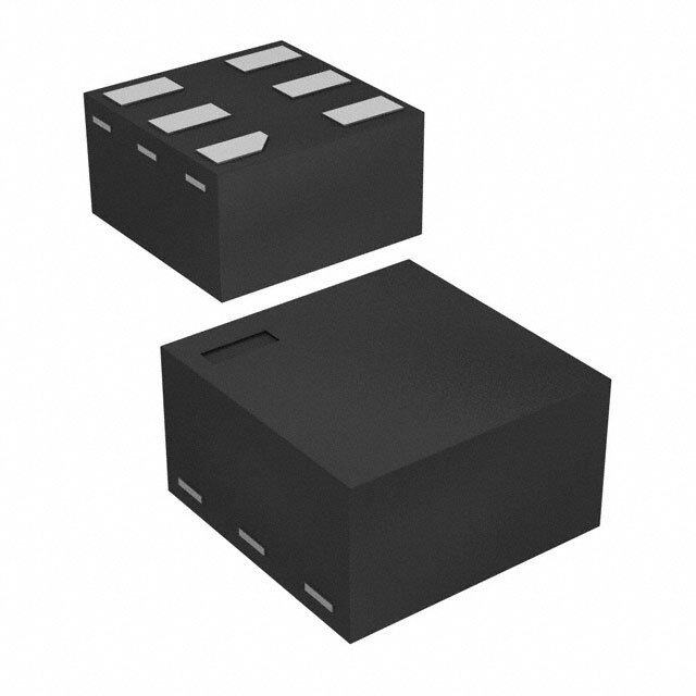
| 产品图片 |
|
| rohs | 符合RoHS无铅 / 符合限制有害物质指令(RoHS)规范要求 |
| 产品系列 | 逻辑集成电路,缓冲器和线路驱动器,Texas Instruments CY74FCT2541CTQCT74FCT |
| 数据手册 | |
| 产品型号 | CY74FCT2541CTQCT |
| 产品种类 | 缓冲器和线路驱动器 |
| 传播延迟时间 | 4.1 ns at 5 V |
| 低电平输出电流 | 12 mA |
| 供应商器件封装 | 20-SSOP/QSOP |
| 元件数 | 1 |
| 其它名称 | 296-22066-2 |
| 包装 | 带卷 (TR) |
| 单位重量 | 125.800 mg |
| 商标 | Texas Instruments |
| 安装类型 | 表面贴装 |
| 安装风格 | SMD/SMT |
| 封装 | Reel |
| 封装/外壳 | 20-SSOP(0.154",3.90mm 宽) |
| 封装/箱体 | SSOP-20 |
| 工作温度 | -40°C ~ 85°C |
| 工厂包装数量 | 2500 |
| 最大工作温度 | + 85 C |
| 最小工作温度 | - 40 C |
| 极性 | Non-Inverting |
| 标准包装 | 2,500 |
| 每元件位数 | 8 |
| 每芯片的通道数量 | 8 |
| 电压-电源 | 4.75 V ~ 5.25 V |
| 电流-输出高,低 | 15mA,12mA |
| 电源电压-最大 | 5.25 V |
| 电源电压-最小 | 4.75 V |
| 电源电流 | 0.0002 mA |
| 系列 | CY74FCT2541T |
| 输入线路数量 | 8 |
| 输出类型 | 3-State |
| 输出线路数量 | 3 |
| 逻辑类型 | 缓冲器/线路驱动器,非反相 |
| 逻辑系列 | FCT |
| 高电平输出电流 | - 15 mA |


PDF Datasheet 数据手册内容提取
(cid:1)(cid:2)(cid:3)(cid:4)(cid:5)(cid:1)(cid:6)(cid:7)(cid:8)(cid:4)(cid:9)(cid:6) (cid:10)(cid:11)(cid:12)(cid:13)(cid:6) (cid:12)(cid:15)(cid:5)(cid:5)(cid:16)(cid:17)(cid:18)(cid:19)(cid:13)(cid:20)(cid:16) (cid:21)(cid:17)(cid:13)(cid:22)(cid:16)(cid:17) (cid:23)(cid:13)(cid:6)(cid:24) (cid:25)(cid:11)(cid:26)(cid:6)(cid:27)(cid:6)(cid:16) (cid:28)(cid:15)(cid:6)(cid:29)(cid:15)(cid:6)(cid:26) SCCS041B – SEPTEMBER 1994 – REVISED SEPTEMBER 2001 (cid:1) Function and Pinout Compatible With FCT Q OR SO PACKAGE and F Logic (TOP VIEW) (cid:1) 25-Ω Output Series Resistors to Reduce OEA 1 20 VCC Transmission-Line Reflection Noise D0 2 19 OEB (cid:1) Reduced VOH (Typically = 3.3 V) Versions D1 3 18 O0 of Equivalent FCT Functions D2 4 17 O1 (cid:1) Edge-Rate Control Circuitry for D3 5 16 O2 Significantly Improved Noise D 6 15 O 4 3 Characteristics D 7 14 O 5 4 (cid:1) Ioff Supports Partial-Power-Down Mode D6 8 13 O5 Operation D7 9 12 O6 (cid:1) GND 10 11 O ESD Protection Exceeds JESD 22 7 – 2000-V Human-Body Model (A114-A) – 200-V Machine Model (A115-A) – 1000-V Charged-Device Model (C101) (cid:1) Matched Rise and Fall Times (cid:1) Fully Compatible With TTL Input and Output Logic Levels (cid:1) 12-mA Output Sink Current 15-mA Output Source Current (cid:1) 3-State Outputs description The CY74FCT2541T is an octal buffer and line driver designed to be employed as a memory-address driver, clock driver, and bus-oriented transmitter/receiver. On-chip termination resistors at the outputs reduce system noise caused by reflections. The CY74FCT2541T can replace the CY74FCT541T to reduce noise in an existing design. The speed of the CY74FCT2541T is comparable to bipolar logic counterparts, while reducing power dissipation. Input and output voltage levels allow direct interface with TTL and CMOS devices without external components. This device is fully specified for partial-power-down applications using I . The I circuitry disables the outputs, off off preventing damaging current backflow through the device when it is powered down. ORDERING INFORMATION SPEED ORDERABLE TOP-SIDE TA PACKAGE† (ns) PART NUMBER MARKING QSOP – Q Tape and reel 4.1 CY74FCT2541CTQCT FCT2541C Tube 4.1 CY74FCT2541CTSOC SSOOIICC – SSOO FFCCTT22554411CC Tape and reel 4.1 CY74FCT2541CTSOCT QSOP – Q Tape and reel 4.8 CY74FCT2541ATQCT FCT2541A –4400°CC ttoo 8855°CC Tube 4.8 CY74FCT2541ATSOC SSOOIICC – SSOO FFCCTT22554411AA Tape and reel 4.8 CY74FCT2541ATSOCT QSOP – Q Tape and reel 8 CY74FCT2541TQCT FCT2541 Tube 8 CY74FCT2541TSOC SSOOIICC – SSOO FFCCTT22554411 Tape and reel 8 CY74FCT2541TSOCT †Package drawings, standard packing quantities, thermal data, symbolization, and PCB design guidelines are available at www.ti.com/sc/package. Please be aware that an important notice concerning availability, standard warranty, and use in critical applications of TexasInstruments semiconductor products and disclaimers thereto appears at the end of this data sheet. (cid:29)(cid:17)(cid:28)(cid:21)(cid:15)(cid:1)(cid:6)(cid:13)(cid:28)(cid:20) (cid:21)(cid:27)(cid:6)(cid:27) (cid:30)(cid:31) !"#$%(cid:30)!(cid:31) (cid:30)& ’("")(cid:31)% $& ! *(+,(cid:30)’$%(cid:30)!(cid:31) -$%). Copyright 2001, Texas Instruments Incorporated (cid:29)"!-(’%& ’!(cid:31) !"# %! &*)’(cid:30) (cid:30)’$%(cid:30)!(cid:31)& *)" %/) %)"#& ! (cid:6))0$& (cid:13)(cid:31)&%"(#)(cid:31)%& &%$(cid:31)-$"- 1$""$(cid:31)%2. (cid:29)"!-(’%(cid:30)!(cid:31) *"!’)&&(cid:30)(cid:31)3 -!)& (cid:31)!% (cid:31))’)&&$"(cid:30),2 (cid:30)(cid:31)’,(-) %)&%(cid:30)(cid:31)3 ! $,, *$"$#)%)"&. POST OFFICE BOX 655303 • DALLAS, TEXAS 75265 1
(cid:1)(cid:2)(cid:3)(cid:4)(cid:5)(cid:1)(cid:6)(cid:7)(cid:8)(cid:4)(cid:9)(cid:6) (cid:10)(cid:11)(cid:12)(cid:13)(cid:6) (cid:12)(cid:15)(cid:5)(cid:5)(cid:16)(cid:17)(cid:18)(cid:19)(cid:13)(cid:20)(cid:16) (cid:21)(cid:17)(cid:13)(cid:22)(cid:16)(cid:17) (cid:23)(cid:13)(cid:6)(cid:24) (cid:25)(cid:11)(cid:26)(cid:6)(cid:27)(cid:6)(cid:16) (cid:28)(cid:15)(cid:6)(cid:29)(cid:15)(cid:6)(cid:26) SCCS041B – SEPTEMBER 1994 – REVISED SEPTEMBER 2001 FUNCTION TABLE INPUTS OOUUTTPPUUTT OEA OEB D L L L L L L H H H H X Z H = High logic level, L = Low logic level, X = Don’t care, Z = High-impedance state logic diagram (positive logic) 1 OEA 19 OEB 2 18 D0 O0 3 17 D1 O1 4 16 D2 O2 5 15 D3 O3 6 14 D4 O4 7 13 D5 O5 8 12 D6 O6 9 11 D7 O7 absolute maximum rating over operating free-air temperature range (unless otherwise noted)† Supply voltage range to ground potential . . . . . . . . . . . . . . . . . . . . . . . . . . . . . . . . . . . . . . . . . . . . . –0.5 V to 7 V DC input voltage range . . . . . . . . . . . . . . . . . . . . . . . . . . . . . . . . . . . . . . . . . . . . . . . . . . . . . . . . . . . . –0.5 V to 7 V DC output voltage range . . . . . . . . . . . . . . . . . . . . . . . . . . . . . . . . . . . . . . . . . . . . . . . . . . . . . . . . . . . –0.5 V to 7 V DC output current (maximum sink current/pin) . . . . . . . . . . . . . . . . . . . . . . . . . . . . . . . . . . . . . . . . . . . . . 120 mA Package thermal impedance, (cid:1) (see Note 1): Q package . . . . . . . . . . . . . . . . . . . . . . . . . . . . . . . . . 68°C/W JA SO package . . . . . . . . . . . . . . . . . . . . . . . . . . . . . . . . 58°C/W Ambient temperature range with power applied, T . . . . . . . . . . . . . . . . . . . . . . . . . . . . . . . . . . –65°C to 135°C A Storage temperature range, T . . . . . . . . . . . . . . . . . . . . . . . . . . . . . . . . . . . . . . . . . . . . . . . . . . –65°C to 150°C stg †Stresses beyond those listed under “absolute maximum ratings” may cause permanent damage to the device. These are stress ratings only, and functional operation of the device at these or any other conditions beyond those indicated under “recommended operating conditions” is not implied. Exposure to absolute-maximum-rated conditions for extended periods may affect device reliability. NOTE 1: The package thermal impedance is calculated in accordance with JESD 51-7. 2 POST OFFICE BOX 655303 • DALLAS, TEXAS 75265
(cid:1)(cid:2)(cid:3)(cid:4)(cid:5)(cid:1)(cid:6)(cid:7)(cid:8)(cid:4)(cid:9)(cid:6) (cid:10)(cid:11)(cid:12)(cid:13)(cid:6) (cid:12)(cid:15)(cid:5)(cid:5)(cid:16)(cid:17)(cid:18)(cid:19)(cid:13)(cid:20)(cid:16) (cid:21)(cid:17)(cid:13)(cid:22)(cid:16)(cid:17) (cid:23)(cid:13)(cid:6)(cid:24) (cid:25)(cid:11)(cid:26)(cid:6)(cid:27)(cid:6)(cid:16) (cid:28)(cid:15)(cid:6)(cid:29)(cid:15)(cid:6)(cid:26) SCCS041B – SEPTEMBER 1994 – REVISED SEPTEMBER 2001 recommended operating conditions (see Note 2) MIN NOM MAX UNIT VCC Supply voltage 4.75 5 5.25 V VIH High-level input voltage 2 V VIL Low-level input voltage 0.8 V IOH High-level output current –15 mA IOL Low-level output current 12 mA TA Operating free-air temperature –40 85 °C NOTE 2: All unused inputs of the device must be held at VCC or GND to ensure proper device operation. POST OFFICE BOX 655303 • DALLAS, TEXAS 75265 3
(cid:1)(cid:2)(cid:3)(cid:4)(cid:5)(cid:1)(cid:6)(cid:7)(cid:8)(cid:4)(cid:9)(cid:6) (cid:10)(cid:11)(cid:12)(cid:13)(cid:6) (cid:12)(cid:15)(cid:5)(cid:5)(cid:16)(cid:17)(cid:18)(cid:19)(cid:13)(cid:20)(cid:16) (cid:21)(cid:17)(cid:13)(cid:22)(cid:16)(cid:17) (cid:23)(cid:13)(cid:6)(cid:24) (cid:25)(cid:11)(cid:26)(cid:6)(cid:27)(cid:6)(cid:16) (cid:28)(cid:15)(cid:6)(cid:29)(cid:15)(cid:6)(cid:26) SCCS041B – SEPTEMBER 1994 – REVISED SEPTEMBER 2001 electrical characteristics over recommended operating free-air temperature range (unless otherwise noted) PARAMETER TEST CONDITIONS MIN TYP† MAX UNIT VIK VCC = 4.75 V, IIN = –18 mA –0.7 –1.2 V VOH VCC = 4.75 V, IOH = –15 mA 2.4 3.3 V VOL VCC = 4.75 V, IOL = 12 mA 0.3 0.55 V Rout VCC = 4.75 V, IOL = 12 mA 20 25 40 Ω Vhys All inputs 0.2 V II VCC = 5.25 V, VIN = VCC 5 µA IIH VCC = 5.25 V, VIN = 2.7 V ±1 µA IIL VCC = 5.25 V, VIN = 0.5 V ±1 µA IOZH VCC = 5.25 V, VOUT = 2.7 V 15 µA IOZL VCC = 5.25 V, VOUT = 0.5 V –15 µA IOS‡ VCC = 5.25 V, VOUT = 0 V –60 –120 –225 mA Ioff VCC = 0 V, VOUT = 4.5 V ±1 µA ICC VCC = 5.25 V, VIN ≤ 0.2 V, VIN ≥VCC – 0.2 V 0.1 0.2 mA ∆ICC VCC = 5.25 V, VIN = 3.4 V§, f1 = 0, Outputs open 0.5 2 mA ICCD¶ VOCECA == 5O.E25B V= aGt N5D0%, V dINut y≤ c0y.2c leV, oOr uVtpINu≥tsV oCpCe n–, 0O.2n eV bit switching, 0.06 0.12 MmHAz/ One bit switching VIN ≤ 0.2 V or VIN ≥VCC– 0.2 V 0.7 1.4 aatt ff11 = 1100 MMHHzz, VCC = 5.25 V, at 50% duty cycle VIN = 3.4 V or GND 1 2.4 IIC## OOuuttppuuttss ooppeenn, mmAA OEAA = OEBB = GND Eight bits switching VIN ≤ 0.2 V or VIN ≥VCC – 0.2 V 1.3 2.6|| aatt ff11 = 22.55 MMHHzz, at 50% duty cycle VIN = 3.4 V or GND 3.3 10.6|| Ci 5 10 pF Co 9 12 pF †Typical values are at VCC = 5 V, TA = 25°C. ‡Not more than one output should be shorted at a time. Duration of short should not exceed one second. The use of high-speed test apparatus and/or sample-and-hold techniques are preferable to minimize internal chip heating and more accurately reflect operational values. Otherwise, prolonged shorting of a high output can raise the chip temperature well above normal and cause invalid readings in other parametric tests. In any sequence of parameter tests, IOS tests should be performed last. §Per TTL-driven input (VIN = 3.4 V); all other inputs at VCC or GND ¶This parameter is derived for use in total power-supply calculations. #IC = ICC + ∆ICC × DH × NT + ICCD (f0/2 + f1 × N1) Where: IC = Total supply current ICC = Power-supply current with CMOS input levels ∆ICC = Power-supply current for a TTL high input (VIN = 3.4 V) DH = Duty cycle for TTL inputs high NT = Number of TTL inputs at DH ICCD = Dynamic current caused by an input transition pair (HLH or LHL) f0 = Clock frequency for registered devices, otherwise zero f1 = Input signal frequency N1 = Number of inputs changing at f1 All currents are in milliamperes and all frequencies are in megahertz. ||Values for these conditions are examples of the ICC formula. 4 POST OFFICE BOX 655303 • DALLAS, TEXAS 75265
(cid:1)(cid:2)(cid:3)(cid:4)(cid:5)(cid:1)(cid:6)(cid:7)(cid:8)(cid:4)(cid:9)(cid:6) (cid:10)(cid:11)(cid:12)(cid:13)(cid:6) (cid:12)(cid:15)(cid:5)(cid:5)(cid:16)(cid:17)(cid:18)(cid:19)(cid:13)(cid:20)(cid:16) (cid:21)(cid:17)(cid:13)(cid:22)(cid:16)(cid:17) (cid:23)(cid:13)(cid:6)(cid:24) (cid:25)(cid:11)(cid:26)(cid:6)(cid:27)(cid:6)(cid:16) (cid:28)(cid:15)(cid:6)(cid:29)(cid:15)(cid:6)(cid:26) SCCS041B – SEPTEMBER 1994 – REVISED SEPTEMBER 2001 switching characteristics over operating free-air temperature range (see Figure 1) FFRROOMM TTOO CY74FCT2541T CY74FCT2541AT CY74FCT2541CT PPAARRAAMMEETTEERR UUNNIITT (INPUT) (OUTPUT) MIN MAX MIN MAX MIN MAX tPLH 1.5 8 1.5 4.8 1.5 4.1 DD OO nnss tPHL 1.5 8 1.5 4.8 1.5 4.1 tPZH 1.5 10 1.5 6.2 1.5 5.8 OOEE OO nnss tPZL 1.5 10 1.5 6.2 1.5 5.8 tPHZ 1.5 9.5 1.5 5.6 1.5 5.2 OOEE OO nnss tPLZ 1.5 9.5 1.5 5.6 1.5 5.2 POST OFFICE BOX 655303 • DALLAS, TEXAS 75265 5
(cid:1)(cid:2)(cid:3)(cid:4)(cid:5)(cid:1)(cid:6)(cid:7)(cid:8)(cid:4)(cid:9)(cid:6) (cid:10)(cid:11)(cid:12)(cid:13)(cid:6) (cid:12)(cid:15)(cid:5)(cid:5)(cid:16)(cid:17)(cid:18)(cid:19)(cid:13)(cid:20)(cid:16) (cid:21)(cid:17)(cid:13)(cid:22)(cid:16)(cid:17) (cid:23)(cid:13)(cid:6)(cid:24) (cid:25)(cid:11)(cid:26)(cid:6)(cid:27)(cid:6)(cid:16) (cid:28)(cid:15)(cid:6)(cid:29)(cid:15)(cid:6)(cid:26) SCCS041B – SEPTEMBER 1994 – REVISED SEPTEMBER 2001 PARAMETER MEASUREMENT INFORMATION 7 V 500 Ω S1 Open From Output Test From Output Under Test Point Under Test GND TEST S1 (sCeeL N= o5t0e pAF) 500 Ω (sCeeL N= o5t0e pAF) 500 Ω ttPPLLHZ//ttPPZHLL O7p Ven tPHZ/tPZH Open LOAD CIRCUIT FOR LOAD CIRCUIT FOR TOTEM-POLE OUTPUTS 3-STATE OUTPUTS 3 V Timing Input 1.5 V tw 0 V th 3 V tsu 3 V Input 1.5 V 1.5 V Data Input 1.5 V 1.5 V 0 V 0 V VOLTAGE WAVEFORMS VOLTAGE WAVEFORMS PULSE DURATION SETUP AND HOLD TIMES 3 V 3 V Output Input 1.5 V 1.5 V Control 1.5 V 1.5 V 0 V 0 V tPLH tPHL tPZL tPLZ In-Phase VOH Output ≈3.5 V Output 1.5 V 1.5 V Waveform 1 1.5 V VOL + 0.3 V VOL (see Note B) VOL tPHL tPLH tPZH tPHZ VOH Output VOH Out-of-Phase 1.5 V 1.5 V Waveform 2 1.5 V VOH – 0.3 V Output VOL (see Note B) ≈0 V VOLTAGE WAVEFORMS VOLTAGE WAVEFORMS PROPAGATION DELAY TIMES ENABLE AND DISABLE TIMES INVERTING AND NONINVERTING OUTPUTS LOW- AND HIGH-LEVEL ENABLING NOTES: A. CL includes probe and jig capacitance. B. Waveform 1 is for an output with internal conditions such that the output is low except when disabled by the output control. Waveform 2 is for an output with internal conditions such that the output is high except when disabled by the output control. C. The outputs are measured one at a time with one input transition per measurement. Figure 1. Load Circuit and Voltage Waveforms 6 POST OFFICE BOX 655303 • DALLAS, TEXAS 75265
PACKAGE OPTION ADDENDUM www.ti.com 6-Feb-2020 PACKAGING INFORMATION Orderable Device Status Package Type Package Pins Package Eco Plan Lead/Ball Finish MSL Peak Temp Op Temp (°C) Device Marking Samples (1) Drawing Qty (2) (6) (3) (4/5) CY74FCT2541ATQCT ACTIVE SSOP DBQ 20 2500 Green (RoHS NIPDAU Level-2-260C-1 YEAR -40 to 85 FCT2541A & no Sb/Br) CY74FCT2541ATQCTE4 ACTIVE SSOP DBQ 20 2500 Green (RoHS NIPDAU Level-2-260C-1 YEAR -40 to 85 FCT2541A & no Sb/Br) CY74FCT2541ATSOC ACTIVE SOIC DW 20 25 Green (RoHS NIPDAU Level-1-260C-UNLIM -40 to 85 FCT2541A & no Sb/Br) CY74FCT2541CTQCT ACTIVE SSOP DBQ 20 2500 Green (RoHS NIPDAU Level-2-260C-1 YEAR -40 to 85 FCT2541C & no Sb/Br) CY74FCT2541CTSOC ACTIVE SOIC DW 20 25 Green (RoHS NIPDAU Level-1-260C-UNLIM -40 to 85 FCT2541C & no Sb/Br) CY74FCT2541TQCT ACTIVE SSOP DBQ 20 2500 Green (RoHS NIPDAU Level-2-260C-1 YEAR -40 to 85 FCT2541 & no Sb/Br) CY74FCT2541TQCTE4 ACTIVE SSOP DBQ 20 2500 Green (RoHS NIPDAU Level-2-260C-1 YEAR -40 to 85 FCT2541 & no Sb/Br) CY74FCT2541TQCTG4 ACTIVE SSOP DBQ 20 2500 Green (RoHS NIPDAU Level-2-260C-1 YEAR -40 to 85 FCT2541 & no Sb/Br) CY74FCT2541TSOC ACTIVE SOIC DW 20 25 Green (RoHS NIPDAU Level-1-260C-UNLIM -40 to 85 FCT2541 & no Sb/Br) CY74FCT2541TSOCE4 ACTIVE SOIC DW 20 25 Green (RoHS NIPDAU Level-1-260C-UNLIM -40 to 85 FCT2541 & no Sb/Br) CY74FCT2541TSOCT ACTIVE SOIC DW 20 2000 Green (RoHS NIPDAU Level-1-260C-UNLIM -40 to 85 FCT2541 & no Sb/Br) (1) The marketing status values are defined as follows: ACTIVE: Product device recommended for new designs. LIFEBUY: TI has announced that the device will be discontinued, and a lifetime-buy period is in effect. NRND: Not recommended for new designs. Device is in production to support existing customers, but TI does not recommend using this part in a new design. PREVIEW: Device has been announced but is not in production. Samples may or may not be available. OBSOLETE: TI has discontinued the production of the device. (2) RoHS: TI defines "RoHS" to mean semiconductor products that are compliant with the current EU RoHS requirements for all 10 RoHS substances, including the requirement that RoHS substance do not exceed 0.1% by weight in homogeneous materials. Where designed to be soldered at high temperatures, "RoHS" products are suitable for use in specified lead-free processes. TI may reference these types of products as "Pb-Free". RoHS Exempt: TI defines "RoHS Exempt" to mean products that contain lead but are compliant with EU RoHS pursuant to a specific EU RoHS exemption. Green: TI defines "Green" to mean the content of Chlorine (Cl) and Bromine (Br) based flame retardants meet JS709B low halogen requirements of <=1000ppm threshold. Antimony trioxide based flame retardants must also meet the <=1000ppm threshold requirement. Addendum-Page 1
PACKAGE OPTION ADDENDUM www.ti.com 6-Feb-2020 (3) MSL, Peak Temp. - The Moisture Sensitivity Level rating according to the JEDEC industry standard classifications, and peak solder temperature. (4) There may be additional marking, which relates to the logo, the lot trace code information, or the environmental category on the device. (5) Multiple Device Markings will be inside parentheses. Only one Device Marking contained in parentheses and separated by a "~" will appear on a device. If a line is indented then it is a continuation of the previous line and the two combined represent the entire Device Marking for that device. (6) Lead/Ball Finish - Orderable Devices may have multiple material finish options. Finish options are separated by a vertical ruled line. Lead/Ball Finish values may wrap to two lines if the finish value exceeds the maximum column width. Important Information and Disclaimer:The information provided on this page represents TI's knowledge and belief as of the date that it is provided. TI bases its knowledge and belief on information provided by third parties, and makes no representation or warranty as to the accuracy of such information. Efforts are underway to better integrate information from third parties. TI has taken and continues to take reasonable steps to provide representative and accurate information but may not have conducted destructive testing or chemical analysis on incoming materials and chemicals. TI and TI suppliers consider certain information to be proprietary, and thus CAS numbers and other limited information may not be available for release. In no event shall TI's liability arising out of such information exceed the total purchase price of the TI part(s) at issue in this document sold by TI to Customer on an annual basis. Addendum-Page 2
PACKAGE MATERIALS INFORMATION www.ti.com 16-Aug-2012 TAPE AND REEL INFORMATION *Alldimensionsarenominal Device Package Package Pins SPQ Reel Reel A0 B0 K0 P1 W Pin1 Type Drawing Diameter Width (mm) (mm) (mm) (mm) (mm) Quadrant (mm) W1(mm) CY74FCT2541ATQCT SSOP DBQ 20 2500 330.0 16.4 6.5 9.0 2.1 8.0 16.0 Q1 CY74FCT2541CTQCT SSOP DBQ 20 2500 330.0 16.4 6.5 9.0 2.1 8.0 16.0 Q1 CY74FCT2541TQCT SSOP DBQ 20 2500 330.0 16.4 6.5 9.0 2.1 8.0 16.0 Q1 CY74FCT2541TSOCT SOIC DW 20 2000 330.0 24.4 10.8 13.0 2.7 12.0 24.0 Q1 PackMaterials-Page1
PACKAGE MATERIALS INFORMATION www.ti.com 16-Aug-2012 *Alldimensionsarenominal Device PackageType PackageDrawing Pins SPQ Length(mm) Width(mm) Height(mm) CY74FCT2541ATQCT SSOP DBQ 20 2500 367.0 367.0 38.0 CY74FCT2541CTQCT SSOP DBQ 20 2500 367.0 367.0 38.0 CY74FCT2541TQCT SSOP DBQ 20 2500 367.0 367.0 38.0 CY74FCT2541TSOCT SOIC DW 20 2000 367.0 367.0 45.0 PackMaterials-Page2
None
None
PACKAGE OUTLINE DW0020A SOIC - 2.65 mm max height SCALE 1.200 SOIC C 10.63 SEATING PLANE TYP 9.97 A PIN 1 ID 0.1 C AREA 18X 1.27 20 1 13.0 2X 12.6 11.43 NOTE 3 10 11 0.51 20X 7.6 0.31 2.65 MAX B 7.4 0.25 C A B NOTE 4 0.33 TYP 0.10 0.25 SEE DETAIL A GAGE PLANE 0.3 1.27 0 - 8 0.1 0.40 DETAIL A TYPICAL 4220724/A 05/2016 NOTES: 1. All linear dimensions are in millimeters. Dimensions in parenthesis are for reference only. Dimensioning and tolerancing per ASME Y14.5M. 2. This drawing is subject to change without notice. 3. This dimension does not include mold flash, protrusions, or gate burrs. Mold flash, protrusions, or gate burrs shall not exceed 0.15 mm per side. 4. This dimension does not include interlead flash. Interlead flash shall not exceed 0.43 mm per side. 5. Reference JEDEC registration MS-013. www.ti.com
EXAMPLE BOARD LAYOUT DW0020A SOIC - 2.65 mm max height SOIC 20X (2) SYMM 1 20 20X (0.6) 18X (1.27) SYMM (R0.05) TYP 10 11 (9.3) LAND PATTERN EXAMPLE SCALE:6X SOOPLEDNEINRG MASK METAL MSOELTDAEL RU NMDAESRK SOOPLEDNEINRG MASK 0.07 MAX 0.07 MIN ALL AROUND ALL AROUND NON SOLDER MASK SOLDER MASK DEFINED DEFINED SOLDER MASK DETAILS 4220724/A 05/2016 NOTES: (continued) 6. Publication IPC-7351 may have alternate designs. 7. Solder mask tolerances between and around signal pads can vary based on board fabrication site. www.ti.com
EXAMPLE STENCIL DESIGN DW0020A SOIC - 2.65 mm max height SOIC 20X (2) SYMM 1 20 20X (0.6) 18X (1.27) SYMM 10 11 (9.3) SOLDER PASTE EXAMPLE BASED ON 0.125 mm THICK STENCIL SCALE:6X 4220724/A 05/2016 NOTES: (continued) 8. Laser cutting apertures with trapezoidal walls and rounded corners may offer better paste release. IPC-7525 may have alternate design recommendations. 9. Board assembly site may have different recommendations for stencil design. www.ti.com
IMPORTANTNOTICEANDDISCLAIMER TI PROVIDES TECHNICAL AND RELIABILITY DATA (INCLUDING DATASHEETS), DESIGN RESOURCES (INCLUDING REFERENCE DESIGNS), APPLICATION OR OTHER DESIGN ADVICE, WEB TOOLS, SAFETY INFORMATION, AND OTHER RESOURCES “AS IS” AND WITH ALL FAULTS, AND DISCLAIMS ALL WARRANTIES, EXPRESS AND IMPLIED, INCLUDING WITHOUT LIMITATION ANY IMPLIED WARRANTIES OF MERCHANTABILITY, FITNESS FOR A PARTICULAR PURPOSE OR NON-INFRINGEMENT OF THIRD PARTY INTELLECTUAL PROPERTY RIGHTS. These resources are intended for skilled developers designing with TI products. You are solely responsible for (1) selecting the appropriate TI products for your application, (2) designing, validating and testing your application, and (3) ensuring your application meets applicable standards, and any other safety, security, or other requirements. These resources are subject to change without notice. TI grants you permission to use these resources only for development of an application that uses the TI products described in the resource. Other reproduction and display of these resources is prohibited. No license is granted to any other TI intellectual property right or to any third party intellectual property right. TI disclaims responsibility for, and you will fully indemnify TI and its representatives against, any claims, damages, costs, losses, and liabilities arising out of your use of these resources. TI’s products are provided subject to TI’s Terms of Sale (www.ti.com/legal/termsofsale.html) or other applicable terms available either on ti.com or provided in conjunction with such TI products. TI’s provision of these resources does not expand or otherwise alter TI’s applicable warranties or warranty disclaimers for TI products. Mailing Address: Texas Instruments, Post Office Box 655303, Dallas, Texas 75265 Copyright © 2020, Texas Instruments Incorporated