ICGOO在线商城 > CY22801KFXI
- 型号: CY22801KFXI
- 制造商: Cypress Semiconductor
- 库位|库存: xxxx|xxxx
- 要求:
| 数量阶梯 | 香港交货 | 国内含税 |
| +xxxx | $xxxx | ¥xxxx |
查看当月历史价格
查看今年历史价格
CY22801KFXI产品简介:
ICGOO电子元器件商城为您提供CY22801KFXI由Cypress Semiconductor设计生产,在icgoo商城现货销售,并且可以通过原厂、代理商等渠道进行代购。 提供CY22801KFXI价格参考以及Cypress SemiconductorCY22801KFXI封装/规格参数等产品信息。 你可以下载CY22801KFXI参考资料、Datasheet数据手册功能说明书, 资料中有CY22801KFXI详细功能的应用电路图电压和使用方法及教程。
| 参数 | 数值 |
| 产品目录 | 集成电路 (IC)半导体 |
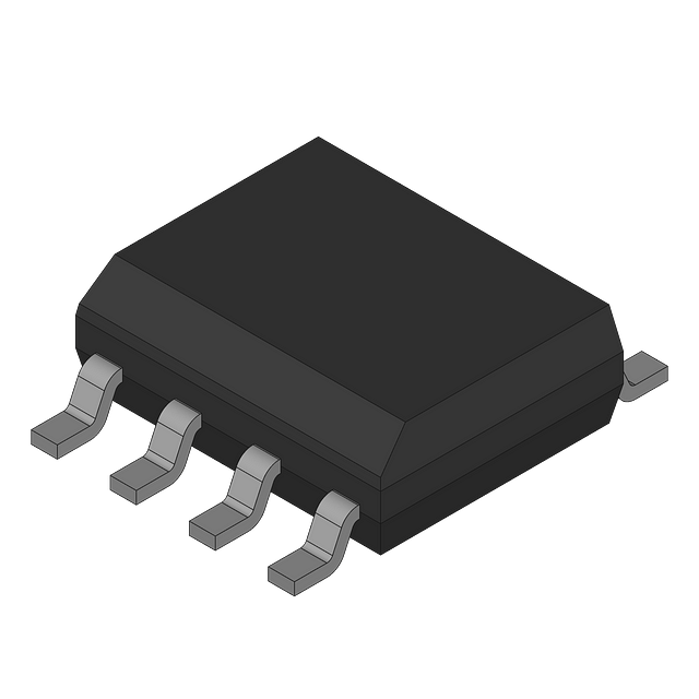
| 描述 | IC CLOCK GEN PROG UNIV 8-SOIC时钟发生器及支持产品 Prog Clk Gen 1MHz-133MHz |
| 产品分类 | |
| 品牌 | Cypress Semiconductor Corp |
| 产品手册 | http://www.cypress.com/?docID=38684 |
| 产品图片 |
|
| rohs | 符合RoHS无铅 / 符合限制有害物质指令(RoHS)规范要求 |
| 产品系列 | 时钟和计时器IC,时钟发生器及支持产品,Cypress Semiconductor CY22801KFXI- |
| 数据手册 | http://www.cypress.com/?docID=38684 |
| 产品型号 | CY22801KFXI |
| PCN组件/产地 | http://www.cypress.com/?docID=44762http://www.cypress.com/?docID=49128 |
| PLL | 是 |
| 产品种类 | 时钟发生器及支持产品 |
| 供应商器件封装 | 8-SOIC |
| 分频器/倍频器 | 是/无 |
| 包装 | 管件 |
| 商标 | Cypress Semiconductor |
| 安装类型 | 表面贴装 |
| 安装风格 | SMD/SMT |
| 封装 | Tube |
| 封装/外壳 | 8-SOIC(0.154",3.90mm 宽) |
| 封装/箱体 | SOIC-8 |
| 工作温度 | -40°C ~ 85°C |
| 工作电源电压 | 3.3 V |
| 工厂包装数量 | 97 |
| 差分-输入:输出 | 无/无 |
| 最大工作温度 | + 70 C |
| 最小工作温度 | 0 C |
| 标准包装 | 97 |
| 比率-输入:输出 | 1:3 |
| 电压-电源 | 3.14 V ~ 3.47 V |
| 电路数 | 1 |
| 类型 | 扇出配送,多路复用器,扩展频谱时钟发生器 |
| 系列 | CY22801KFXI |
| 输入 | 时钟,晶体 |
| 输出 | LVCMOS |
| 频率-最大值 | 166.6MHz |



- 商务部:美国ITC正式对集成电路等产品启动337调查
- 曝三星4nm工艺存在良率问题 高通将骁龙8 Gen1或转产台积电
- 太阳诱电将投资9.5亿元在常州建新厂生产MLCC 预计2023年完工
- 英特尔发布欧洲新工厂建设计划 深化IDM 2.0 战略
- 台积电先进制程称霸业界 有大客户加持明年业绩稳了
- 达到5530亿美元!SIA预计今年全球半导体销售额将创下新高
- 英特尔拟将自动驾驶子公司Mobileye上市 估值或超500亿美元
- 三星加码芯片和SET,合并消费电子和移动部门,撤换高东真等 CEO
- 三星电子宣布重大人事变动 还合并消费电子和移动部门
- 海关总署:前11个月进口集成电路产品价值2.52万亿元 增长14.8%


.jpg)
PDF Datasheet 数据手册内容提取
CY22801 Universal Programmable Clock Generator (UPCG) Universal Programmable Clock Generator (UPCG) Features Functional Description ■Integrated phase-locked loop (PLL) The CY22801 is a flash-programmable clock generator that supports various applications in consumer and communications ■Field-Programmable markets. The device uses the Cypress-proprietary PLL along ■Input frequency range: with Spread Spectrum and VCXO technology to make it one of the most versatile clock synthesizers in the market. The device ❐Crystal: 8 MHz to 30 MHz uses a Cypress-proprietary PLL to drive up to three configurable ❐CLKIN: 1 MHz to 133 MHz outputs in an 8-pin SOIC. ■Low-voltage complementary metal oxide semiconductor The CY22801 is programmed with an easy-to-use programmer (LVCMOS) output frequency: dongle, the CY36800, in conjunction with the CyClocksRT™ ❐Up to 200 MHz (commercial grade) software. This enables fast sample generation of prototype ❐Up to 166.6 MHz (industrial grade) builds for user-defined frequencies. Cypress’s value-added distribution partners and third-party programming systems from ■Special Features: BP Microsystems, HiLo Systems, and others, can also be ❐Spread Spectrum contacted for large production quantities. A JEDEC file needs to ❐VCXO be configured to program CY22801, which can be generated ❐Inputs: PD or OE, FS using the CyClocksRT™ software. ■Low-jitter, high-accuracy outputs For a complete list of related documentation, click here. ■3.3 V operation ■Commercial and industrial temperature ranges ■8-pin small-outline integrated circuit (SOIC) package ■Serial interface for device configuration Logic Block Diagram XIN/CLKIN XOUT VCXO REF PLL Divider CLKA with Logic 1 SDAT/FS0/ VCXO VCXO/OE /PD# Switch CLKB/ FS1/ Serial I/F Matrix FS2 SCLK SCLK with /FS1 SDAT Control Divider CLKC /FS0 /PD# Logic 2 /FS2 OE CypressSemiconductorCorporation • 198 Champion Court • SanJose, CA 95134-1709 • 408-943-2600 Document Number: 001-15571 Rev. *M Revised January 3, 2018
CY22801 Contents Pin Configurations ...........................................................3 CyClocksRT Software ....................................................12 Pin Definitions ..................................................................3 Possible Configuration Examples ................................12 External Reference Crystal/Clock Input .........................4 Informational Graphs .....................................................13 Output Clock Frequencies ...............................................4 Absolute Maximum Conditions .....................................14 VCXO .................................................................................4 Recommended Operating Conditions ..........................14 VCXO Profile ...............................................................4 Recommended Crystal Specifications Spread Spectrum Clock Generation (SSCG) .................4 for non-VCXO Applications ...........................................14 Spread Percentage .....................................................4 Pullable Crystal Specifications Modulation Frequency .................................................4 for VCXO Application only .............................................14 SSON Pin ....................................................................4 DC Electrical Specifications ..........................................15 Multifunction Pins ............................................................5 AC Electrical Characteristics ........................................16 Frequency Calculation and Register Definitions ...........5 Test Circuit ......................................................................17 Default Startup Condition for the CY22801 ....................6 Timing Definitions ..........................................................17 Frequency Calculations and Register Definitions 2-wire Serial (I2C) Interface Timing ...............................18 using the Serial (I2C) Interface ........................................6 Data Valid ..................................................................18 Reference Frequency ..................................................6 Data Frame ...............................................................18 Programmable Crystal Input Oscillator Acknowledge Pulse ...................................................18 Gain Settings ......................................................................6 Ordering Information ......................................................20 Using an External Clock as the Reference Input .........7 Possible Configurations .............................................20 Input Load Capacitors .................................................8 Ordering Code Definitions .........................................20 PLL Frequency, Q Counter [42H(6..0)] .......................8 Package Diagram ............................................................21 PLL Frequency, P Counter Acronyms ........................................................................22 [40H(1..0)], [41H(7..0)], [42H(7)] .........................................9 Document Conventions .................................................22 PLL Post Divider Options [0CH(7..0)], [47H(7..0)] .......9 Units of Measure .......................................................22 Charge Pump Settings [40H(2..0)] ..............................9 Document History Page .................................................23 Clock Output Settings: CLKSRC Sales, Solutions, and Legal Information ......................26 – Clock Output Crosspoint Switch Matrix Worldwide Sales and Design Support .......................26 [44H(7..0)], [45H(7..0)], [46H(7..6)] ...................................10 Products ....................................................................26 Test, Reserved, and Blank Registers ........................10 PSoC® Solutions ......................................................26 Application Guideline .....................................................12 Cypress Developer Community .................................26 Best Practices for Best Jitter Performance ................12 Technical Support .....................................................26 Field Programming the CY22801 ..................................12 Document Number: 001-15571 Rev. *M Page 2 of 26
CY22801 Pin Configurations Figure 1. CY22801 8-pin SOIC pinout XIN/CLKIN 1 8 XOUT V 2 7 CLKC/FS2 DD CY22801 SDAT/FS0/ 3 6 CLKA VCXO/OE/PD# V 4 5 CLKB/FS1/SCLK SS Pin Definitions Name Pin Number Description CLKIN / 1 External reference crystal input / external reference clock input XIN V 2 3.3 V voltage supply DD SDAT / FS0 3 Serial interface data line / frequency select 0 / VCXO analog control voltage / Output Enable / / VCXO / Power-down OE / PD# V 4 Ground SS CLKB / FS1 5 Clock output B / frequency select 1 / serial interface clock line / SCLK CLKA 6 Clock output A CLKC / 7 Clock output C / frequency select 3 / V SS FS2 XOUT 8 External reference crystal output: Connect to external crystal. When the reference is an external clock signal (applied to pin 1), this pin is not used and must be left floating. Document Number: 001-15571 Rev. *M Page 3 of 26
CY22801 External Reference Crystal/Clock Input VCXO is not compatible with Spread spectrum and Serial Interface. CY22801 can accept external reference clock input as well as VCXO Profile crystal input. External reference clock input frequency range is from 1 MHz to 133 MHz. Figure3 shows an example of a VCXO profile. The analog The input crystal oscillator of the CY22801 is an important voltage input is on the X-axis and the PPM range is on the Y-axis. feature because of the flexibility it provides in selecting a crystal An increase in the VCXO input voltage results in a corresponding as a reference clock source. The oscillator inverter has increase in the output frequency. This moves the PPM from a programmable gain, enabling maximum compatibility with a negative to positive offset. reference crystal, based on manufacturer, process, Figure 3. VCXO Profile performance, and quality. Input load capacitors are placed on the CY22801 die to reduce 200 external component cost. These capacitors are true parallel-plate capacitors, designed to reduce the frequency shift 150 that occurs when non-linear load capacitance is affected by load, 100 bias, supply, and temperature changes. m] 50 p p The value of the input load capacitors is determined by eight bits g [ 0 in a programmable register. Total load capacitance is determined unin -500 0.5 1 1.5 2 2.5 3 3.5 by the formula: T -100 CapLoad = (CL – CBRD – CCHIP) / 0.09375 pF -150 In CyClocksRT, enter the crystal capacitance (C ). The value of -200 L CapLoad is determined automatically and programmed into the VCXO input [V] CY22801. Output Clock Frequencies Spread Spectrum Clock Generation (SSCG) The CY22801 is a very flexible clock generator with up to three individual outputs, generated from an integrated PLL. See Spread spectrum clock generation (SSCG) in CY22801 helps to Figure2 for details. reduce EMI found in today’s high-speed digital electronic The output of the PLL runs at high frequency and is divided down systems. to generate the output clocks. Two programmable dividers are The device uses the proprietary spread spectrum clock (SSC) available for this purpose. Therefore, although the output clocks technology to synthesize and modulate the frequency of the may have different frequencies, they must be related, based on input clock. By modulating the frequency of the clock, the the PLL frequency. measured EMI at the fundamental and harmonic frequencies is It is also possible to direct the reference clock input to any of the greatly reduced. This reduction in radiated energy can outputs, thereby bypassing the PLL. Lastly, the reference clock significantly reduce the cost of complying with the regulatory may be passed through either divider. agency electromagnetic compatibility (EMC) requirements and improve time to market without degrading system performance. Figure 2. Basic PLL Block Diagram Programmed spread spectrum modulation will appear same on all three clock outputs as they come from same PLL even if Post Divider operating at different frequencies. Spread spectrum is not (XINR/CELFKIN) /Q PFD VCO 1N CLKA compatible with VCXO feature. /P Post CrSowssitpcohint CLKB Spread Percentage Divider Matrix CLKC 2N The percentage of spread can be programmed from ±0.25% to ±2.5% for center spread and from –0.5% to –5.0% for down spread. The granularity is 0.25%. Modulation Frequency VCXO The default modulation frequency is 31.5 kHz. Other modulation frequencies available through configuration software are One of the key components of the CY22801 device is the VCXO. 30.1kHz and 32.9 kHz. The VCXO is used to ‘pull’ the reference crystal higher or lower to lock the system frequency to an external source. This is ideal SSON Pin for applications where the output frequency needs to track along SSON pin functionality can be used to turn Spread ON and OFF with an external reference frequency that is constantly shifting. in clock output. Any one of the Multifunction pins can be A special pullable crystal must be used to have adequate VCXO configured as SSON pin. pull range. Pullable crystal specifications are included in this datasheet. Document Number: 001-15571 Rev. *M Page 4 of 26
CY22801 Multifunction Pins Table 2. Possible Combinations for Multifunction Pins There are three pins [1] with multiple functions either as control pins or as output pins. The following are the acronyms used for Possible Combinations Pin#3 Pin#5 Pin#7 the different control function pins: A FS0 CLKB CLKC ■Output enable (OE): If OE = 1, all outputs are enabled B FS0 CLKB FS2 ■Frequency select (FS0, 1, 2): These pins can be used to select C FS0 FS1 FS2 one of the programmed clock frequencies for clock output. All D OE / PD# CLKB CLKC of three multifunction pins support this functionality. Any of these pins can also be configured as Spread spectrum ON E OE / PD# FS1 CLKC (SSON) pin. If SSON = 1, clock output has programmed F OE / PD# FS1 FS2 spread; if SSON = 0, clock output does not have spread. G SDAT SCLK CLKC ■Power-down: active low (PD#): If PD# = 0, all outputs are H VCXO CLKB CLKC tristated and the device enters in the low-power state ■Voltage controlled crystal oscillator (VCXO): Analog voltage on Frequency Calculation and Register this pin controls the output frequency of oscillator Definitions ■Serial interface clock line (SCLK) and serial interface data line (SDAT): These pins are for serial interface and are compatible The CY22801 is an extremely flexible clock generator with four with I2C. basic variables that are used to determine the final output frequency. They are the input reference frequency (REF), the Each of these three multi-function pins supports selected internally calculated P and Q dividers, and the post divider, which functions mentioned in Table1. One of the supported functions can be a fixed or calculated value. There are three formulas to can be programmed on the pin at a time. determine the final output frequency of a CY22801 based design: Table 1. Multi Function Pin Options ■CLK = ((REF × P) / Q) / Post divider Pin# Pin Name OE PD# VCXO FS CLK I2C ■CLK = REF / Post divider OUTPUT 3 SDAT / FS0 / Y Y Y[2] Y[3] N[4] SDAT[2] ■CLK = REF VCXO / OE / The basic PLL block diagram is shown in Figure 4 on page 6. PD# Each of the three clock outputs on the CY22801 has a total of 5 CLKB / FS1 / N N N Y Y SCLK seven output options available to it. There are six post divider SCLK options available: /2 (two of these), /3, /4, /DIV1N and /DIV2N. 7 CLKC / FS2 N N N Y Y[5] N DIV1N and DIV2N are independently calculated and are applied to individual output groups. The post divider options can be applied to the calculated VCO frequency ((REF × P) / Q) or to the REF directly. In addition to the six post divider output options, the seventh option bypasses the PLL and passes the REF directly to the crosspoint switch matrix. Notes 1. There are Weak Pull up resistors (approximately 100 k) on all Multifunctional pins. 2. VCXO and SSON functions as well as VCXO and Serial Interface functions are not compatible. 3. ‘Y’ means pin supports this function. 4. ‘N’ means pin does not support this function. 5. Do not use this pin as Reference Clock Output. Document Number: 001-15571 Rev. *M Page 5 of 26
CY22801 Figure 4. Basic Block Diagram of CY22801 PLL DIV1N[0CH] CLKSRC Crosspoint DIV1SRC[0CH] Divider Bank 1 Switch Matrix Qtotal /DIV1N REF (Q+2) PFD VCO /2 [45H] CLKA [42H] DIV Ptotal 1C /3 L (2(PB+4)+PO) KDivider Bank 2 [44H, 45H] CLKB [40H, 41H, 42H] /DIV2N /4 D IV [45H, 46H] CLKC 2C /2 L K DIV2SRC[47H] DIV1N[47H] CLKOE[09H] Default Startup Condition for the CY22801 All programmable registers in the CY22801 are addressed with eight bits and contain eight bits of data. The CY22801 is a slave The default (programmed) condition of the device is generally set device with an address of 1101001 (69H). by the distributor who programs the device using a customer Table 3 on page 7 lists the I2C registers and their definitions. specific JEDEC file produced by CyClocksRT. Parts shipped Specific register definitions and their allowable values are listed from the factory are blank and unprogrammed. In this condition, as follows. all bits are set to 0, all outputs are three-stated, and the crystal oscillator circuit is active. Reference Frequency While you can develop your own subroutine to program any or The REF can be a crystal or a driven frequency (CLKIN). For all of the individual registers described in the following pages, it crystals, the frequency range must be between 8 MHz and may be easier to use CyClocksRT to produce the required 30MHz. For a driven frequency, the frequency range must be register setting file [6]. between 1 MHz and 133 MHz. The serial interface address of the CY22801 is 69H. If there is a Programmable Crystal Input Oscillator Gain Settings conflict with any other devices in your system, then this can also be changed [7, 8]. The Input crystal oscillator gain (XDRV) is controlled by two bits in register 12H and are set according to Table 4 on page 8. The Frequency Calculations and Register parameters controlling the gain are the crystal frequency, the Definitions using the Serial (I2C) Interface internal crystal parasitic resistance (ESR, available from the manufacturer), and the CapLoad setting during crystal startup. The CY22801 provides an industry standard serial interface for Bits 3 and 4 of register 12H control the input crystal oscillator gain volatile, in-system programming of unique frequencies and setting. Bit 4 is the MSB of the setting, and bit 3 is the LSB. The options. Serial programming and re-programming allows for setting is programmed according to Table 4 on page 8. All other quick design changes and product enhancements, eliminates bits in the register are reserved and should be programmed as inventory of old design parts, and simplifies manufacturing. shown in Table 5 on page 8. The I2C Interface provides volatile programming. This means FTAAddrSrc[1:0] bits set Frequency tuning array address when the target system is powered down, the CY22801 reverts source. This will be set by CyClockRT software based on to its pre-I2C state, as defined above (programmed or selected configuration. unprogrammed). When the system is powered back up again, the I2C registers must be reconfigured again. Notes 6. Advanced features like VCXO, SCL, SDA, FS, OE, SSON are not supported by CyClocksRT. Contact your local Cypress field application engineer for functional feasibility and custom configuration with these advanced features. 7. Please Contact your local Cypress FAE, if you need serial interface address other than 69H. 8. while configuring Jedec through CyClocksRT software, if Pin3 (SDAT) and Pin5 (SCLK) is not configured for any functionality, the jedec file automatically gets configured with I2C Enable Functionality with default I2C address as 69 H. Document Number: 001-15571 Rev. *M Page 6 of 26
CY22801 Using an External Clock as the Reference Input The CY22801 also accepts an external clock as reference, with speeds up to 133 MHz. With an external clock, the XDRV (register 12H) bits must be set according to Table 6 on page 8. Table 3. Summary Table – CY22801 Programmable Registers Register Description D7 D6 D5 D4 D3 D2 D1 D0 09H CLKOE control 0 0 CLKC CLKA 0 CLKB 0 0 OCH DIV1SRC mux and DIV1N DIV1SRC DIV1N (6) DIV1N (5) DIV1N (4) DIV1N (3) DIV1N (2) DIV1N (1) DIV1N (0) divider 12H Input crystal oscillator drive FTAAddrSrc[1] FTAAddrSrc[0] XCapSrc XDRV (1) XDRV (0) 0 0 0 control 13H Input load capacitor control CapLoad (7) CapLoad (6) CapLoad (5) CapLoad (4) CapLoad (3) CapLoad (2) CapLoad (1) CapLoad (0) 40H Charge pump and PB 1 1 0 Pump (2) Pump (1) Pump (0) PB (9) PB (8) counter 41H PB (7) PB (6) PB (5) PB (4) PB (3) PB (2) PB (1) PB (0) 42H PO counter, Q counter PO Q (6) Q (5) Q (4) Q (3) Q (2) Q (1) Q (0) 44H Crosspoint switch matrix 1 1 1 1 1 1 CLKSRC2 for CLKSRC1 for control CLKB CLKB 45H CLKSRC0 for 1 1 1 CLKSRC2 for CLKSRC1 for CLKSRC0 for CLKSRC2 for CLKB CLKA CLKA CLKA CLKC 46H CLKSRC1 for CLKSRC0 for 1 1 1 1 1 1 CLKC CLKC 47H DIV2SRC mux and DIV2N DIV2SRC DIV2N(6) DIV2N(5) DIV2N(4) DIV2N(3) DIV2N(2) DIV2N(1) DIV2N(0) divider Document Number: 001-15571 Rev. *M Page 7 of 26
CY22801 Table 4. Programmable Crystal Input Oscillator Gain Settings Cap Register Settings 00H–80H 80H–C0H C0H–FFH Effective Load Capacitance 6 pF to 12 pF 12 pF to 18 pF 18 pF to 30 pF (CapLoad) Crystal ESR 30 60 30 60 30 60 Crystal input 8 to 15 MHz 00 01 01 10 01 10 frequency 15 to 20 MHz 01 10 01 10 10 10 20 to 25 MHz 01 10 10 10 10 11 25 to 30 MHz 10 10 10 11 11 N/A Table 5. Crystal Oscillator Gain Bit Locations and Values Address D7 D6 D5 D4 D3 D2 D1 D0 12H 0 0 1 XDRV(1) XDRV(0) 0 0 0 Table 6. Programmable External Reference Input Oscillator Drive Settings Reference Frequency 1 to 25 MHz 25 to 50 MHz 50 to 90 MHz 90 to 133 MHz Drive Setting 00 01 10 11 Input Load Capacitors In CyClocksRT, enter the crystal capacitance (C ). The value of L CapLoad is determined automatically and programmed into the XCapSrc bit in 12H register selects the source of Input load CY22801. Through the SDAT and SCLK pins, the value can be capacitance. This will be set by CyClockRT software based on adjusted up or down if your board capacitance is greater or less selected configuration. than 2 pF. For an external clock source, CapLoad defaults to 0. Input load capacitors allow you to set the load capacitance of the See Table 7 on page 9 for CapLoad bit locations and values. CY22801 to match the input load capacitance from a crystal. The The input load capacitors are placed on the CY22801 die to value of the input load capacitors is determined by 8 bits in a reduce external component cost. These capacitors are true programmable register [13H]. Total load capacitance is parallel-plate capacitors, designed to reduce the frequency shift determined by the formula: that occurs when nonlinear load capacitance is affected by load, CapLoad = (CL– CBRD – CCHIP) / 0.09375 pF bias, supply, and temperature changes. where: PLL Frequency, Q Counter [42H(6..0)] ■C = specified load capacitance of your crystal. L The first counter is known as the Q counter. The Q counter ■CBRD = the total board capacitance, due to external capacitors divides REF by its calculated value. Q is a 7 bit divider with a and board trace capacitance. In CyClocksRT, this value maximum value of 127 and minimum value of 0. The primary defaults to 2 pF. value of Q is determined by 7 bits in register 42H (6..0), but 2 is ■CCHIP = 6 pF. added to this register value to achieve the total Q, or Qtotal. Qtotal is defined by the formula: ■0.09375 pF = the step resolution available due to the 8-bit register. Qtotal = Q + 2 In CyclocksRT, only the crystal capacitance (CL) is specified. The minimum value of Qtotal is 2. The maximum value of Qtotal is C is set to 6 pF and C defaults to 2 pF. If your board 129. Register 42H is defined in the table. CHIP BRD capacitance is higher or lower than 2 pF, the formula given earlier Stable operation of the CY22801 cannot be guaranteed if is used to calculate a new CapLoad value and programmed into REF/Q falls below 250 kHz. Q bit locations and values are total total register 13H. defined in Table 8 on page 9. Document Number: 001-15571 Rev. *M Page 8 of 26
CY22801 PLL Frequency, P Counter [40H(1..0)], [41H(7..0)], output frequency. The mux determines if the clock signal feeding [42H(7)] into the divider banks is the calculated VCO frequency or REF. There are two select muxes (DIV1SRC and DIV2SRC) and two The next counter definition is the P (product) counter. The P divider banks (Divider Bank 1 and Divider Bank 2) used to counter is multiplied with the (REF/Q ) value to achieve the total determine this clock signal. The clock signal passing through VCO frequency. The product counter, defined as P , is made total DIV1SRC and DIV2SRC is referred to as DIV1CLK and up of two internal variables, PB and PO. The formula for DIV2CLK, respectively. calculating P is: total The divider banks have four unique divider options available: /2, P = (2(PB + 4) + PO) total /3, /4, and /DIVxN. DIVxN is a variable that can be independently PB is a 10-bit variable, defined by registers 40H(1:0) and programmed (DIV1N and DIV2N) for each of the two divider 41H(7:0). The 2 LSBs of register 40H are the two MSBs of banks. The minimum value of DIVxN is 4. The maximum value variable PB. Bits 4..2 of register 40H are used to determine the of DIVxN is 127. A value of DIVxN below 4 is not guaranteed to charge pump settings. The three MSBs of register 40H are work properly. preset and reserved and cannot be changed. PO is a single bit DIV1SRC is a single bit variable, controlled by register 0CH. The variable, defined in register 42H(7). This allows for odd numbers remaining seven bits of register 0CH determine the value of post in P . total divider DIV1N. The remaining seven bits of 42H are used to define the DIV2SRC is a single bit variable, controlled by register 47H. The Qcounter, as shown in Table8. remaining seven bits of register 47H determine the value of post The minimum value of P is 8. The maximum value of P is divider DIV2N. total total 2055. To achieve the minimum value of P , PB and PO should total Register 0CH and 47H are defined in Table9. both be programmed to 0. To achieve the maximum value of P , PB should be programmed to 1023, and PO should be Charge Pump Settings [40H(2..0)] total programmed to 1. The correct pump setting is important for PLL stability. Charge Stable operation of the CY22801 cannot be guaranteed if the pump settings are controlled by bits (4..2) of register 40H, and value of (P × (REF/Q )) is above 400MHz or below are dependent on internal variable PB (see “PLL Frequency, P total total 100MHz. Counter[40H(1..0)], [41H(7..0)], [42H(7)]”). Table 10 on page 10 summarizes the proper charge pump settings, based on Ptotal. PLL Post Divider Options [0CH(7..0)], [47H(7..0)] See Table 11 on page 10 for register 40H bit locations and The output of the VCO is routed through two independent values. muxes, then to two divider banks to determine the final clock Table 7. Input Load Capacitor Register Bit Settings Address D7 D6 D5 D4 D3 D2 D1 D0 13H CapLoad(7) CapLoad(6) CapLoad(5) CapLoad(4) CapLoad(3) CapLoad(2) CapLoad(1) CapLoad(0) Table 8. P Counter and Q Counter Register Definition Address D7 D6 D5 D4 D3 D2 D1 D0 40H 1 1 0 Pump(2) Pump(1) Pump(0) PB(9) PB(8) 41H PB(7) PB(6) PB(5) PB(4) PB(3) PB(2) PB(1) PB(0) 42H PO Q(6) Q(5) Q(4) Q(3) Q(2) Q(1) Q(0) Table 9. PLL Post Divider Options Address D7 D6 D5 D4 D3 D2 D1 D0 0CH DIV1SRC DIV1N(6) DIV1N(5) DIV1N(4) DIV1N(3) DIV1N(2) DIV1N(1) DIV1N(0) 47H DIV2SRC DIV2N(6) DIV2N(5) DIV2N(4) DIV2N(3) DIV2N(2) DIV2N(1) DIV2N(0) Document Number: 001-15571 Rev. *M Page 9 of 26
CY22801 Table 10. Charge Pump Settings Charge Pump Setting – Pump(2..0) Calculated P total 000 16–44 001 45–479 010 480–639 011 640–799 100 800–1023 101, 110, 111 Do not use – device will be unstable Table 11. Register 40H Change Pump Bit Settings Address D7 D6 D5 D4 D3 D2 D1 D0 40H 1 1 0 Pump(2) Pump(1) Pump(0) PB(9) PB(8) Although using the above table guarantees stability, it is guaranteed to be rising edge phase-aligned with recommended to use the Print preview function in CyClocksRT CLKSRC(0,0,1). to determine the correct charge pump settings for optimal jitter When DIV2N is divisible by four, then CLKSRC(1,0,1) is performance. guaranteed to be rising edge phase-aligned with PLL stability cannot be guaranteed for values below 16 and CLKSRC(1,0,0). When DIV2N is divisible by eight, then above 1023. If values above 1023 are needed, use CyClocksRT CLKSRC(1,1,0) is guaranteed to be rising edge phase-aligned to determine the best charge pump setting. To configure device with CLKSRC(1,0,0). using serial interface, please refer CyClocksRT. CLKOE – Clock Output Enable Control [09H(5..0)] Clock Output Settings: CLKSRC – Clock Output Each clock output has its own output enable, controlled by Crosspoint Switch Matrix [44H(7..0)], [45H(7..0)], register 09H(5..0). To enable an output, set the corresponding [46H(7..6)] CLKOE bit to 1. CLKOE settings are in Table 14 on page 11. Every clock output can be defined to come from one of seven Test, Reserved, and Blank Registers unique frequency sources. The CLKSRC(2..0) crosspoint switch matrix defines which source is attached to each individual clock Writing to any of the following registers causes the part to exhibit output. CLKSRC(2..0) is set in Registers 44H, 45H, and 46H. abnormal behavior, as follows. The remainder of register 46H(5:0) must be written with the [00H to 08H] – Reserved values stated in the register table when writing register values [0AH to 0BH] – Reserved 46H(7:6). [0DH to 11H] – Reserved When DIV1N is divisible by four, then CLKSRC(0,1,0) is [14H to 3FH] – Reserved guaranteed to be rising edge phase-aligned with [43H] – Reserved CLKSRC(0,0,1). When DIV1N is six, then CLKSRC(0,1,1) is [48H to FFH] – Reserved. Table 12. Clock Output Setting CLKSRC2 CLKSRC1 CLKSRC0 Definition and Notes 0 0 0 Reference input. 0 0 1 DIV1CLK/DIV1N. DIV1N is defined by register [OCH]. Allowable values for DIV1N are 4 to 127. If Divider Bank 1 is not being used, set DIV1N to 8. 0 1 0 DIV1CLK/2. Fixed /2 divider option. If this option is used, DIV1N must be divisible by 4. 0 1 1 DIV1CLK/3. Fixed /3 divider option. If this option is used, set DIV1N to 6. 1 0 0 DIV2CLK/DIV2N. DIV2N is defined by Register [47H]. Allowable values for DIV2N are 4 to 127. If Divider Bank 2 is not being used, set DIV2N to 8. 1 0 1 DIV2CLK/2. Fixed /2 divider option. If this option is used, DIV2N must be divisible by 4. 1 1 0 DIV2CLK/4. Fixed /4 divider option. If this option is used, DIV2N must be divisible by 8. 1 1 1 Reserved – do not use. Document Number: 001-15571 Rev. *M Page 10 of 26
CY22801 Table 13. Clock Output Register Setting Address D7 D6 D5 D4 D3 D2 D1 D0 44H 1 1 1 1 1 1 CLKSRC2 CLKSRC1 for CLKB for CLKB 45H CLKSRC0 1 1 1 CLKSRC2 CLKSRC1 CLKSRC0 CLKSRC2 for CLKB for CLKA for CLKA for CLKA for CLKC 46H CLKSRC1 CLKSRC0 1 1 1 1 1 1 for CLKC for CLKC Table 14. CLKOE Bit Setting Address D7 D6 D5 D4 D3 D2 D1 D0 09H 0 0 CLKC CLKA 0 CLKB 0 0 Document Number: 001-15571 Rev. *M Page 11 of 26
CY22801 Application Guideline Field Programming the CY22801 Best Practices for Best Jitter Performance The CY22801 is programmed using the CY36800 USB programmer dongle. The CY22801 is flash-technology based, so Jitter can be specified in different terminologies: the parts are reprogrammed up to 100 times. This enables fast Time Domain: and easy design changes and product updates, and eliminates any issues with old and out-of-date inventory. ■Cycle-to-cycle jitter Samples and small prototype quantities are programmed using ■Period jitter the CY36800 programmer. Cypress’s value-added distribution partners and third-party programming systems from BP ■Long-term jitter Microsystems, HiLo Systems, and others, can also be contacted Frequency domain: for large production quantities. Third-Party Programmer List can be found at below link http://www.cypress.com/?rID=14364. ■Deterministic jitter ■Random jitter CyClocksRT Software ■Phase noise CyClocksRT is an easy-to-use software application that enables These jitter terms are usually given in terms of root mean square the user to custom-configure the CY22801. Users can specify (RMS), peak-to-peak, or in the case of phase noise, dBC/Hz with the XIN/CLKIN frequency, crystal load capacitance, and output respect to fundamental frequency. Cycle-to-cycle and period frequencies. CyClocksRT then creates an industry-standard jitter are generally used terminologies. Jitter depends on many JEDEC file that is used to program the CY22801[6]. factors and few of the them can be controlled in application: When needed, an advanced mode is available that enables ■Input reference jitter users to override the automatically generated voltage controlled oscillator (VCO) frequency and output divider values. ■Number of active clock outputs CyClocksRT is a component of the CyberClocks™ software that ■Operating temperature you can download free of charge from the Cypress website at http://www.cypress.com. ■Clock output load CY36800 InstaClock™ Kit ■PLL frequencies The Cypress CY36800 InstaClock kit comes with everything ■Termination and layout needed to design the CY22801 and program samples and small ■Supply voltage accuracy prototype quantities. The CyClocksRT software is used to quickly create a JEDEC programming file, which is then Jitter is directly proportional to the input reference jitter, number downloaded directly to the portable programmer that is included of active clock outputs, operating temperature and clock output in the CY36800 InstaClock kit. The JEDEC file can also be saved load, but inversely proportional to the PLL frequency. Best for use in a production programming system for larger volumes. practices for termination, layout and supply voltage filtering are discussed in application note “Layout and Termination The CY36800 also comes with five samples of the CY22801, Techniques For Cypress Clock Generators – AN1111”. which are programmed with preconfigured JEDEC files using the InstaClock software. Possible Configuration Examples Table 15. Possible Configuration Possible Configurations Pin#1 Pin#3 Pin#5 Pin#6 Pin#7 Pin#8 A CLKIN: 33 MHz OE CLKB: 33 MHz CLKA: SSON NC 100MHz with +/-1% Spread B XIN: 27 MHz VCXO PD# CLKA: 74.25 / FS2 XOUT: 27 MHz crystal 74.175824 MHz crystal C CLKIN: 10 MHz OE FS1 CLKA: 25 / 40 / FS2 NC 33.3333 / 50MHz D CLKIN: 10 MHz SDAT SCLK CLKA CLKB NC Contact your local Cypress field application engineer for functional feasibility and custom configuration with these advanced features. Document Number: 001-15571 Rev. *M Page 12 of 26
CY22801 Informational Graphs The informational graphs are meant to convey the typical performance levels. No performance specifications is implied or guaranteed. 172.5 171.5 Spread Spectrum Profile: Fnom=166MHz, 68.5 Spread Spectrum Profile: Fnom=66MHz, 170.5 Fmod=30kHz, Spread%= -4% 68 Fmod=30kHz, Spread%= -4% 169.5 67.5 168.5 67 167.5 66.5 166.5 Fnominal 66 Fnominal 165.5 65.5 164.5 65 163.5 64.5 162.5 64 161.5 63.5 160.5 159.5 0 20 40 60 80 100 120 140 160 180 200 0 20 40 60 80 100 120 140 160 180 200 Time (us) Time (us) 169.5 169 Spread Spectrum Profile: Fnom=166MHz, 67.5 Spread Spectrum Profile: Fnom=66MHz, 168.5 Fmod=30kHz, Spread%= +/-1% Fmod=30kHz, Spread%= +/-1% 168 67 167.5 167 66.5 166.5 166 Fnominal 66 Fnominal 165.5 65.5 165 164.5 164 65 163.5 163 64.5 162.5 0 20 40 60 80 100 120 140 160 180 200 0 20 40 60 80 100 120 140 160 180 200 Time (us) Time (us) Document Number: 001-15571 Rev. *M Page 13 of 26
CY22801 Absolute Maximum Conditions Parameter Description Min Max Unit V Supply voltage –0.5 4.6 V DD T Storage temperature –65 150 °C S T Junction temperature – 125 °C J V Input and output voltage V – 0.5 V + 0.5 V IO SS DD ESD Electrostatic discharge voltage per MIL-STD-833, Method 3015 2000 – V Recommended Operating Conditions Parameter Description Min Typ Max Unit V Operating voltage 3.14 3.3 3.47 V DD T Ambient temperature, commercial grade 0 – 70 °C A Ambient temperature, industrial grade –40 -- 85 °C C Maximum load capacitance on the CLK output – – 15 pF LOAD t Power-up time for V to reach the minimum specified voltage (power 0.05 – 500 ms PU DD ramps must be monotonic) Recommended Crystal Specifications for non-VCXO Applications Parameter Name Description Min Typ Max Unit F Nominal crystal frequency Parallel resonance, fundamental mode, 8 – 30 MHz NOM and AT cut C Nominal load capacitance 6 – 30 pF LNOM R Equivalent series resistance Fundamental mode – 35 50 1 (ESR) DL Crystal drive level No external series resistor assumed – 0.5 2 mW Pullable Crystal Specifications for VCXO Application only Parameter [9] Name Min Typ Max Unit C Crystal load capacitance – 14 – pF LNOM R Equivalent series resistance – – 25 1 R /R Ratio of third overtone mode ESR to fundamental mode ESR. Ratio is 3 – – – 3 1 used because typical R values are much less than the maximum spec. 1 DL Crystal drive level. No external series resistor assumed – 0.5 2 mW F Third overtone separation from 3 × F (high side) 300 – – ppm 3SEPHI NOM F Third overtone separation from 3 × F (low side) – – –150 ppm 3SEPLO NOM C0 Crystal shunt capacitance 7 pF C0/C1 Ratio of shunt to motional capacitance 180 – 250 C Crystal motional capacitance 14.4 18 21.6 fF 1 Note 9. Crystals that meet this specification include Ecliptek ECX-5788-13.500M, Siward XTL001050A-13.5-14-400, Raltron A-13.500-14-CL, and PDI HA13500XFSA14XC. Document Number: 001-15571 Rev. *M Page 14 of 26
CY22801 DC Electrical Specifications Parameter [10] Name Description Min Typ Max Unit I Output high current V = V – 0.5, V = 3.3 V (source) 12 24 – mA OH OH DD DD I Output low current V = 0.5, V = 3.3 V (sink) 12 24 – mA OL OL DD C Input capacitance All input pins except XIN and XOUT – – 7 pF IN1 C Input capacitance XIN and XOUT pins for non-VCXO – 24 – pF IN2 applications I Input high current V = V – 5 10 A IH IH DD I Input low current V = 0 V – – 50 A IL IL f VCXO pullability range Using crystal in this data sheet ±150 – ppm XO V VCXO input range 0 – V V VCXO DD V Input high voltage CMOS levels, 70% of V 0.7 × V – – V IH DD DD V Input low voltage CMOS levels, 30% of V – – 0.3 × V V IL DD DD IDD[11] VDD supply current All three clock outputs are at 100 MHz – 30 – mA Notes 10.Not 100% tested, guaranteed by design. 11.Power supply current is configuration dependent. Use CyClocksRT to calculate actual IDD for specific output frequency configurations. Document Number: 001-15571 Rev. *M Page 15 of 26
CY22801 AC Electrical Characteristics Parameter [12] Name Description Min Typ Max Unit f Reference frequency - crystal 8 – 30 MHz REFC f Reference frequency - driven 1 – 133 MHz REFD f Output frequency, commercial – – 200 MHz OUT grade Output frequency, industrial – – 166.6 MHz grade DC Output duty cycle 50% of V see Figure6 45 50 55 % DD, t Rising edge slew rate Output clock rise time, 20%–80% of 0.8 1.4 – V/ns 3 V see Figure7 DD, t Falling edge slew rate Output clock fall time, 80%–20% of 0.8 1.4 – V/ns 4 V see Figure7 DD, t [13] Skew Output-output skew between – – 250 ps 5 related outputs, see Figure9 t [14] Clock jitter Peak-to-peak period jitter, see – 250 – ps 6 Figure8 t [14] Cycle-to-cycle jitter CLKA/B/C XIN = CLKA/B/C = 166 MHz, – – 110 ps CCJ ±2% spread and No REFOUT, V = 3.3 V, see Figure10 DD XIN = CLKA/B/C = 66.66 MHz, – – 170 ps ±2% spread and No REFOUT, V = 3.3 V, see Figure10 DD XIN = CLKA/B/C = 33.33 MHz, – – 140 ps ±2% spread and No REFOUT, V = 3.3 V, see Figure10 DD XIN = CLKA/B/C = 14.318 MHz, – – 290 ps ±2% spread and No REFOUT, V = 3.3 V, see Figure10 DD t Power-down time Time from falling edge on PD# pin to – 150 300 ns PD tristated outputs (asynchronous), see Figure11 t Output disable time Time from falling edge on OE pin to – 150 300 ns OE1 tristated outputs (asynchronous), see Figure12 t Output enable time Time from rising edge on OE pin to – 150 300 ns OE2 valid clock outputs (asynchronous), see Figure12 F Spread spectrum modulation 30.1 31.5 32.9 kHz MOD frequency t PLL lock time – – 3 ms 10 Notes 12.Not 100% tested, guaranteed by design. 13.Skew value guaranteed when outputs are generated from the same divider bank. 14.Jitter measurement may vary. Actual jitter is dependent on input jitter and edge rate, number of active outputs, input and output frequencies, supply voltage, temperature, and output load. Document Number: 001-15571 Rev. *M Page 16 of 26
CY22801 Test Circuit Figure 5. Test Circuit Diagram VDD CLKout 0.1F Output CLOAD GND Timing Definitions Figure 6. Duty Cycle Definition; DC = t2/t1 Figure 7. Rise and Fall Time Definitions t1 t3 t4 t2 80% CLK 50% 50% CLK 20% Figure 8. Period Jitter Definition Figure 9. Skew Definition t6 t5 CLKx 50% CLK 50% CLKy 50% Figure 10. Cycle to Cycle Jitter Definition (CCJ) Figure 11. Power-Down and Power-Up Timing TCycle_i TCycle_i+1 PDOOWWENR VIL VIH tPU 50% High CLK CLK Impedance t t = T - T (over 1000 Cycles) PD CCJ Cycle_i Cycle_i+1 Figure 12. Output Enable and Disable Timing EONUATBPLUET VIL VIH tOE2 High CLK Impedance t OE1 Document Number: 001-15571 Rev. *M Page 17 of 26
CY22801 2-wire Serial (I2C) Interface Timing Start Sequence – Start frame is indicated by SDAT going LOW when SCLK is HIGH. Every time a Start signal is given, the next When using I2C interface, the CY22801 should be programmed eight-bit data must be the device address (seven bits) and a R/W as I2C-capable prior to using this interface. bit, followed by the register address (eight bits) and register data (eight bits). The CY22801 uses a 2-wire serial-interface SDAT and SCLK that operates up to 400 kbits/second in read or write mode. The Stop Sequence – Stop frame is indicated by SDAT going HIGH basic write serial format is as follows. when SCLK is HIGH. A Stop frame frees the bus for writing to another part on the same bus or writing to another random Start Bit; seven-bit Device Address (DA); R/W Bit; Slave Clock register address. Acknowledge (ACK); eight-bit Memory Address (MA); ACK; eight-bit data; ACK; eight-bit data in MA + 1 if desired; ACK; Acknowledge Pulse eight-bit data in MA+2; ACK; and so on, until STOP bit. The basic serial format is illustrated in Figure14. During Write mode, the CY22801 responds with an ACK pulse after every eight bits. This is accomplished by pulling the SDAT Data Valid line LOW during the N × 9th clock cycle, as illustrated in Figure16. (N = the number of eight-bit segments transmitted.) Data is valid when the Clock is HIGH, and may only be During Read mode, the ACK pulse, after the data packet is sent, transitional when the clock is LOW, as illustrated in Figure13. is generated by the master. Data Frame Every new data frame is indicated by a start and stop sequence, as illustrated in Figure15. Figure 13. Data Valid and Data Transition Periods Data valid Transition to next bit SDAT V IH SCLK V IL Figure 14. Data Frame Architecture 1-bit 1-bit 1-bit 1-bit 1-bit 1-bit 1-bit 1-bit SDAT Write 1-bit Slave Slave Slave Slave Slave Slave Slave Slave R/W = 0 ACK ACK ACK ACK ACK ACK ACK ACK Multiple 7-bit 8-bit 8-bit 8-bit 8-bit 8-bit 8-bit Contiguous Device RegisterRegisterRegister Register Register Register Registers Address AddressData Data Data Data Data (XXH) (XXH) (XXH+1) (XXH+2) (FFH) (00H) Start Signal Stop Signal 1-bit 1-bit 1-bit 1-bit 1-bit 1-bit 1-bit SDAT Read 1-bit Slave Slave 1-bit Master Master Master Master Master R/W = 0 ACK ACK R/W = 1 ACK ACK ACK ACK NACK Multiple 7-bit 8-bit 8-bit 8-bit 8-bit 8-bit Contiguous Device Register7-Bit Register Register Register Register Registers Address AddressDevice Data Data Data Data (XXH) Address(XXH) (XXH+1) (FFH) (00H) Start Signal Stop Signal Document Number: 001-15571 Rev. *M Page 18 of 26
CY22801 Figure 15. Start and Stop Frame SDAT SCLK Transition START STOP to next bit Figure 16. Frame Format (Device Address, R/W, Register Address, Register Data SDAT + + + START DA6 DA5DA0 R/W ACK RA7 RA6RA1 RA0 ACK D7 D6 D1 D0 ACK STOP SCLK + + + Figure 17. Definition for Timing on the Serial BUS SDAT t t t t t t t t f LOW r SU;DAT f HD;STA r BUF SCLK t t t S HD;STA tHD;DAT tHIGH SU;STA Sr SU;STO P S Table 16. Serial Programming Interface Timing Specifications Parameter Description Min Max Unit f Frequency of SCLK – 400 kHz SCLK t Hold time START condition 0.6 – s HD:STA t Low period of the SCLK clock 1.3 – s LOW t High period of the SCLK clock 0.6 – s HIGH t Setup time for a repeated START condition 0.6 – s SU:STA t Data hold time 100 – ns HD:DAT t Data setup time 100 – ns SU:DAT t Rise time – 300 ns R t Fall time – 300 ns F t Setup time for STOP condition 0.6 – s SU:STO t Bus-free time between STOP and START conditions 1.3 – s BUF Document Number: 001-15571 Rev. *M Page 19 of 26
CY22801 Ordering Information Ordering Code Package Type Operating Range Operating Voltage CY22801KFXC 8-pin SOIC Commercial, 0 °C to 70 °C 3.3 V CY22801KFXCT 8-pin SOIC – Tape and Reel Commercial, 0 °C to 70 °C 3.3 V CY22801KFXI 8-pin SOIC Industrial, –40 °C to 85 °C 3.3 V CY22801KFXIT 8-pin SOIC – Tape and Reel Industrial, –40 °C to 85 °C 3.3 V Some product offerings are factory-programmed customer-specific devices with customized part numbers. The Possible Configurations table shows the available device types, but not complete part numbers. Contact your local Cypress FAE or sales representative for more information. Possible Configurations Ordering Code Package Type Operating Range Operating Voltage CY22801SXC-xxx [15] 8-pin SOIC Commercial, 0 °C to 70 °C 3.3 V CY22801SXC-xxxT [15] 8-pin SOIC – Tape and Reel Commercial, 0 °C to 70 °C 3.3 V CY22801SXI-xxx [15] 8-pin SOIC Industrial, –40 °C to 85 °C 3.3 V CY22801SXI-xxxT [15] 8-pin SOIC – Tape and Reel Industrial, –40 °C to 85 °C 3.3 V CY22801KSXC-xxx [15] 8-pin SOIC Commercial, 0 °C to 70 °C 3.3 V CY22801KSXC-xxxT [15] 8-pin SOIC – Tape and Reel Commercial, 0 °C to 70 °C 3.3 V CY22801KSXI-xxx [15] 8-pin SOIC Industrial, –40 °C to 85 °C 3.3 V CY22801KSXI-xxxT [15] 8-pin SOIC – Tape and Reel Industrial, –40 °C to 85 °C 3.3 V Ordering Code Definitions CY 22801X X X X - xxx X X = blank or T blank = Tube; T = Tape and Reel Custom Configuration Code (Only for Factory Programmable Devices) Temperature Range: X = C or I C = Commercial; I = Industrial Pb-free Programming Option: X = F or blank F = Field Programmable; blank = Factory Programmable Device part number: 22801X = 22801K or 22801 X in Device part number: X = K or none K = Foundry Manufacturing Company ID: CY = Cypress Note 15.Ordering codes with “xxx” are factory-programmed configurations. Factory programming is available for high volume orders. For more details, contact your local Cypress field application engineer or Cypress sales representative. Document Number: 001-15571 Rev. *M Page 20 of 26
CY22801 Package Diagram Figure 18. 8-pin SOIC (150 Mils) S08.15/SZ08.15 Package Outline, 51-85066 51-85066 *I Document Number: 001-15571 Rev. *M Page 21 of 26
CY22801 Acronyms Document Conventions Table 17. Acronyms Used in this Document Units of Measure Acronym Description Table 18. Units of Measure ACK Acknowledge Symbol Unit of Measure CLKIN Clock Input °C degree Celsius CMOS Complementary Metal-Oxide Semiconductor dBc/Hz decibels relative to the carrier per Hertz EMI Electromagnetic Interference fF femtofarad ESD Electrostatic Discharge Hz hertz EMC Electromagnetic Compatibility kbit 1024 bits ESR Equivalent Series Resistance kHz kilohertz FS Frequency Select MHz megahertz I2C Inter Integrated Circuit µA microampere JEDEC Joint Electron Device Engineering Council µF microfarad LSB Least Significant Bit µs microsecond LVCMOS Low-Voltage Complementary Metal Oxide mA milliampere Semiconductor ms millisecond MSB Most Significant Bit mW milliwatt OE Output Enable ns nanosecond PD Power Down ohm PFD Phase Frequency Detector % percent PLL Phase Locked Loop pF picofarad SSON Spread Spectrum ON ppm parts per million SCLK Serial Interface Clock ps picosecond SDAT Serial Interface Data V volt SOIC Small-Outline Integrated Circuit SSC Spread Spectrum Clock SSCG Spread Spectrum Clock Generation UPCG Universal Programmable Clock Generator VCO Voltage Controlled Oscillator VCXO Voltage Controlled Crystal Oscillator Document Number: 001-15571 Rev. *M Page 22 of 26
CY22801 Document History Page Document Title: CY22801, Universal Programmable Clock Generator (UPCG) Document Number: 001-15571 Orig. of Submission Revision ECN Description of Change Change Date ** 1058080 KVM / 05/10/07 New data sheet. KKVTMP *A 2440787 AESA 05/16/08 Updated Ordering Information (Added existing part numbers CY22801FXCT, CY22801FXI, CY22801FXIT, CY22801SXC-xxx and CY22801SXC-xxxT and added new part numbers CY22801KFXC, CY22801KFXCT, CY22801KFXI, CY22801KFXIT, CY22801KSXC-xxx and CY22801KSXC-xxxT, added Note “Not recommended for new designs.” and referred the same note for some ordering codes, Added Note 15 and referred the same note for some ordering codes). Updated to new template. *B 2724806 KVM / 6/26/09 Updated Recommended Operating Conditions (Added T parameter A AESA (Industrial Grade Ambient Temperature) and details). Updated AC Electrical Characteristics (Added f parameter (Industrial OUT Grade Output Frequency) and details). Updated Ordering Information (Removed CY22801FXCT and CY22801FXIT, added CY22801KSXI-xxx and CY22801KSXI-xxxT, added temperature ranges in the Operating Range column in the Ordering Information Table). Updated Package Diagram (Corrected package reference from S8 to SZ08 for the spec 51-85066). *C 2897775 KVM 03/23/10 Updated Ordering Information: Updated part numbers (Removed inactive parts). Added Possible Configurations and moved xxx parts under the same. Updated Package Diagram: spec 51-85066 – Changed revision from *C to *D. *D 2981862 BASH 07/15/2010 Updated Features (Added Special Features). Removed the section Benefits. Updated Logic Block Diagram. Updated Pin Configurations. Updated Pin Definitions. Added VCXO. Added Spread Spectrum Clock Generation (SSCG). Added Multifunction Pins. Added Frequency Calculation and Register Definitions Added Default Startup Condition for the CY22801. Added Frequency Calculations and Register Definitions using the Serial (I2C) Interface. Added Application Guideline. Added Possible Configuration Examples. Added Informational Graphs. Added Pullable Crystal Specifications for VCXO Application only. Updated DC Electrical Specifications (Added I , I , f , V parameters IH IL XO VCXO and their details). Updated AC Electrical Characteristics (Added t , t , t , t , F CCJ PD OE1 OE2 MOD parameters and their details). Updated Timing Definitions (Added Figure8, Figure9, Figure10, Figure11, Figure12). Added 2-wire Serial (I2C) Interface Timing. Updated Ordering Information: Updated Possible Configurations: Updated details in “Ordering Code” column. Added Ordering Code Definitions. Added Acronyms and Units of Measure. Document Number: 001-15571 Rev. *M Page 23 of 26
CY22801 Document History Page (continued) Document Title: CY22801, Universal Programmable Clock Generator (UPCG) Document Number: 001-15571 Orig. of Submission Revision ECN Description of Change Change Date *E 3207656 CXQ 03/28/2011 Updated 2-wire Serial (I2C) Interface Timing: Updated Table16 (Changed minimum value of t parameter from 0 ns to DH 100ns). *F 3455237 BASH / 12/05/2011 Updated Multifunction Pins (Added Note 1 and referred the same note in the PURU first paragraph in the section). Updated Package Diagram: spec 51-85066 – Changed revision from *D to *E. Updated to new template. *G 3580417 PURU 04/12/2012 Updated Features (Removed Field-programmable). Updated Functional Description (Replaced “programming using CY36800” with “programmed using Factory Specific Configurations”). Updated Default Startup Condition for the CY22801 (Added Note 6 and referred the same note at the end of 2nd paragraph in the section, added Note7 and referred the same note at the end of 3rd paragraph in the section). Updated Frequency Calculations and Register Definitions using the Serial (I2C) Interface (Updated PLL Frequency, P Counter [40H(1..0)], [41H(7..0)], [42H(7)] (“Replaced CY22150 with CY22801”)). Updated Field Programming the CY22801 (Replaced “programming using CY36800” with “programmed using Factory Specific Configurations”). Removed the section “CY36800 InstaClock™ Kit”. *H 3686409 PURU 07/20/2012 Updated Features (Added Field-programmable). Updated Functional Description (Replaced “programmed using Factory Specific Configurations” with “programming using CY36800”). Updated Field Programming the CY22801 (Replaced “programmed using Factory Specific Configurations” with “programming using CY36800”). Added the section “CY36800 InstaClock™ Kit”. Updated Default Startup Condition for the CY22801 (Added Note 8 and referred the same note at the end of 3nd paragraph in the section) Updated to new template. *I 4576237 AJU 11/21/2014 Updated Features: Updated details under “Low-voltage complementary metal oxide semiconductor (LVCMOS) output frequency”. Updated Functional Description: Added “For a complete list of related documentation, click here.” at the end. Updated AC Electrical Characteristics: Removed minimum values corresponding to f and f parameters. REFD OUT Updated 2-wire Serial (I2C) Interface Timing: Updated Figure14 (Updated the last ACK in SDAT Read (Multiple Contiguous Registers) to “NACK”. Updated Package Diagram: spec 51-85066 – Changed revision from *E to *F. *J 4632360 TAVA 01/20/2015 Updated Ordering Information: Updated Possible Configurations: Updated details in “Ordering Code” column. Updated to new template. *K 4643649 TAVA 01/28/2015 Updated Ordering Information: Updated Possible Configurations: Updated details in “Ordering Code” column. Updated Package Diagram: spec 51-85066 – Changed revision from *F to *G. Document Number: 001-15571 Rev. *M Page 24 of 26
CY22801 Document History Page (continued) Document Title: CY22801, Universal Programmable Clock Generator (UPCG) Document Number: 001-15571 Orig. of Submission Revision ECN Description of Change Change Date *L 4805790 TAVA 06/26/2015 Updated 2-wire Serial (I2C) Interface Timing: Updated Figure13. Added Figure17. Updated Table16: Updated entire table. Updated to new template. Completing Sunset Review. *M 6012075 PAWK 01/03/2018 Updated Package Diagram: spec 51-85066 – Changed revision from *G to *I. Updated to new template. Document Number: 001-15571 Rev. *M Page 25 of 26
CY22801 Sales, Solutions, and Legal Information Worldwide Sales and Design Support Cypress maintains a worldwide network of offices, solution centers, manufacturer’s representatives, and distributors. To find the office closest to you, visit us at Cypress Locations. Products PSoC® Solutions Arm® Cortex® Microcontrollers cypress.com/arm PSoC 1 | PSoC 3 | PSoC 4 | PSoC 5LP | PSoC 6 MCU Automotive cypress.com/automotive Cypress Developer Community Clocks & Buffers cypress.com/clocks Community | Projects | Video | Blogs | Training | Components Interface cypress.com/interface Technical Support Internet of Things cypress.com/iot cypress.com/support Memory cypress.com/memory Microcontrollers cypress.com/mcu PSoC cypress.com/psoc Power Management ICs cypress.com/pmic Touch Sensing cypress.com/touch USB Controllers cypress.com/usb Wireless Connectivity cypress.com/wireless © Cypress Semiconductor Corporation, 2007-2018. This document is the property of Cypress Semiconductor Corporation and its subsidiaries, including Spansion LLC ("Cypress"). This document, including any software or firmware included or referenced in this document ("Software"), is owned by Cypress under the intellectual property laws and treaties of the United States and other countries worldwide. Cypress reserves all rights under such laws and treaties and does not, except as specifically stated in this paragraph, grant any license under its patents, copyrights, trademarks, or other intellectual property rights. If the Software is not accompanied by a license agreement and you do not otherwise have a written agreement with Cypress governing the use of the Software, then Cypress hereby grants you a personal, non-exclusive, nontransferable license (without the right to sublicense) (1) under its copyright rights in the Software (a) for Software provided in source code form, to modify and reproduce the Software solely for use with Cypress hardware products, only internally within your organization, and (b) to distribute the Software in binary code form externally to end users (either directly or indirectly through resellers and distributors), solely for use on Cypress hardware product units, and (2) under those claims of Cypress's patents that are infringed by the Software (as provided by Cypress, unmodified) to make, use, distribute, and import the Software solely for use with Cypress hardware products. Any other use, reproduction, modification, translation, or compilation of the Software is prohibited. TO THE EXTENT PERMITTED BY APPLICABLE LAW, CYPRESS MAKES NO WARRANTY OF ANY KIND, EXPRESS OR IMPLIED, WITH REGARD TO THIS DOCUMENT OR ANY SOFTWARE OR ACCOMPANYING HARDWARE, INCLUDING, BUT NOT LIMITED TO, THE IMPLIED WARRANTIES OF MERCHANTABILITY AND FITNESS FOR A PARTICULAR PURPOSE. To the extent permitted by applicable law, Cypress reserves the right to make changes to this document without further notice. Cypress does not assume any liability arising out of the application or use of any product or circuit described in this document. Any information provided in this document, including any sample design information or programming code, is provided only for reference purposes. It is the responsibility of the user of this document to properly design, program, and test the functionality and safety of any application made of this information and any resulting product. Cypress products are not designed, intended, or authorized for use as critical components in systems designed or intended for the operation of weapons, weapons systems, nuclear installations, life-support devices or systems, other medical devices or systems (including resuscitation equipment and surgical implants), pollution control or hazardous substances management, or other uses where the failure of the device or system could cause personal injury, death, or property damage ("Unintended Uses"). A critical component is any component of a device or system whose failure to perform can be reasonably expected to cause the failure of the device or system, or to affect its safety or effectiveness. Cypress is not liable, in whole or in part, and you shall and hereby do release Cypress from any claim, damage, or other liability arising from or related to all Unintended Uses of Cypress products. You shall indemnify and hold Cypress harmless from and against all claims, costs, damages, and other liabilities, including claims for personal injury or death, arising from or related to any Unintended Uses of Cypress products. Cypress, the Cypress logo, Spansion, the Spansion logo, and combinations thereof, WICED, PSoC, CapSense, EZ-USB, F-RAM, and Traveo are trademarks or registered trademarks of Cypress in the United States and other countries. For a more complete list of Cypress trademarks, visit cypress.com. Other names and brands may be claimed as property of their respective owners. Document Number: 001-15571 Rev. *M Revised January 3, 2018 Page 26 of 26 CyClocksRT, CyberClocks, and InstaClock are trademarks of Cypress Semiconductor Corporation.
Mouser Electronics Authorized Distributor Click to View Pricing, Inventory, Delivery & Lifecycle Information: C ypress Semiconductor: CY22801SXC-014T CY22801KSXC-011T CY22801FXI CY22801FXC CY22801KFXI CY22801KFXCT CY22801SXI-022 CY22801KSXC-014T CY22801SXC-014 CY22801KSXC-014 CY22801FXIT CY22801KSXC-011 CY22801SXI-022T CY22801FXCT CY22801KFXIT CY22801KFXC CY22801KSXC-018 CY22801KSXC-018T CY22801KSXC-019T CY22801KSXC-024 CY22801KSXI-026T CY22801KSXC-020T CY22801KSXC-020 CY22801KSXC-027T CY22801KSXC-027 CY22801KSXC-021T CY22801KSXC-019 CY22801KSXI-026 CY22801KSXC-021 CY22801KSXC-024T
 Datasheet下载
