ICGOO在线商城 > 集成电路(IC) > 数据采集 - ADCs/DAC - 专用型 > CS5341-CZZ
 Datasheet下载
- 型号: CS5341-CZZ
- 制造商: Cirrus Logic
- 库位|库存: xxxx|xxxx
- 要求:
| 数量阶梯 | 香港交货 | 国内含税 |
| +xxxx | $xxxx | ¥xxxx |
查看当月历史价格
查看今年历史价格
CS5341-CZZ产品简介:
ICGOO电子元器件商城为您提供CS5341-CZZ由Cirrus Logic设计生产,在icgoo商城现货销售,并且可以通过原厂、代理商等渠道进行代购。 CS5341-CZZ价格参考。Cirrus LogicCS5341-CZZ封装/规格:数据采集 - ADCs/DAC - 专用型, ADC,音频 24 b 192k 串行 16-TSSOP。您可以下载CS5341-CZZ参考资料、Datasheet数据手册功能说明书,资料中有CS5341-CZZ 详细功能的应用电路图电压和使用方法及教程。
CS5341-CZZ是Cirrus Logic Inc.生产的一款专用型模数转换器(ADC),主要用于高精度音频信号采集和处理。该器件广泛应用于各类音频设备中,尤其适合对音质要求极高的专业音频系统。

 应用场景:

1. 专业音频设备:
   - CS5341-CZZ常用于高端录音设备、音频接口和混音台等专业音频设备中。其高分辨率和低噪声特性使其能够捕捉到极为细腻的音频细节,确保录制的音频质量达到最佳水平。

2. 家庭影院系统:
   - 在家庭影院系统中,CS5341-CZZ可以用于音频输入模块,提供高质量的音频信号采集,确保用户在观看电影或聆听音乐时获得沉浸式的音效体验。

3. 消费级音响设备:
   - 该芯片也适用于一些高端消费级音响设备,如Hi-Fi音响系统、便携式音乐播放器等,以提升音频信号的采集精度,带来更纯净、逼真的声音表现。

4. 广播与演播室设备:
   - 在广播电台和电视演播室中,CS5341-CZZ可用于麦克风前置放大器、音频处理器等设备,确保音频信号的高保真传输,满足广播级音质的要求。

5. 乐器与音频效果器:
   - 对于电子乐器和音频效果器,CS5341-CZZ可以用于将模拟音频信号转换为数字信号,以便进行进一步的处理和效果添加,同时保持原始音频的高保真度。

6. 语音识别与通信设备:
   - 在语音识别系统和通信设备中,CS5341-CZZ可以用于语音信号的高精度采集,提高语音识别的准确性和通信质量,特别是在嘈杂环境中,其低噪声特性尤为关键。

7. 医疗音频设备:
   - 在某些医疗音频设备中,如助听器和声学监测设备,CS5341-CZZ可以提供高精度的音频信号采集,帮助医生更准确地诊断和治疗听力问题。

 总结:
CS5341-CZZ凭借其高分辨率、低噪声和高动态范围的特点,成为众多专业音频设备和高端消费类音频产品的理想选择。无论是录音棚、家庭影院还是医疗音频设备,它都能提供卓越的音频性能,确保用户获得最优质的音效体验。
| 参数 | 数值 |
| ADC输入端数量 | 2 |
| 产品目录 | 集成电路 (IC)半导体 |
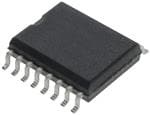
| 描述 | IC ADC 24BIT SRL 192KHZ 16-TSSOP音频模/数转换器 IC 105dB 192 kHz Multi-Bit Audio ADC |
| 产品分类 | |
| 品牌 | Cirrus Logic |
| 产品手册 | |
| 产品图片 |
|
| rohs | 符合RoHS无铅 / 符合限制有害物质指令(RoHS)规范要求 |
| 产品系列 | 音频 IC,音频模/数转换器 IC,Cirrus Logic CS5341-CZZ- |
| 数据手册 | |
| 产品型号 | CS5341-CZZ |
| 产品目录页面 | |
| 产品种类 | 音频模/数转换器 IC |
| 供应商器件封装 | 16-TSSOP |
| 信噪比 | 105 dB |
| 其它名称 | 598-1082-5 |
| 分辨率 | 24 bit |
| 分辨率(位) | 24 b |
| 功耗 | 90 mW |
| 包装 | * |
| 商标 | Cirrus Logic |
| 商标名 | CS534 |
| 安装类型 | 表面贴装 |
| 安装风格 | SMD/SMT |
| 封装 | Tube |
| 封装/外壳 | 16-TSSOP(0.173",4.40mm 宽) |
| 封装/箱体 | TSSOP-16 |
| 工作温度 | -10°C ~ 70°C |
| 工作电源电压 | 3.3 V, 5 V |
| 工厂包装数量 | 96 |
| 数据接口 | 串行 |
| 最大工作温度 | + 70 C |
| 最小工作温度 | - 10 C |
| 标准包装 | 96 |
| 电压-电源 | 3.1 V ~ 5.25 V |
| 电压源 | 模拟和数字 |
| 电源电压-最大 | 5.25 V |
| 电源电压-最小 | 3.1 V |
| 类型 | ADC, 音频 |
| 系列 | CS5341 |
| 转换器数量 | 2 |
| 转换速率 | 192 kS/s |
| 配用 | /product-detail/zh/CDB5341/598-1545-ND/2024829 |
| 采样率(每秒) | 192k |


- 商务部:美国ITC正式对集成电路等产品启动337调查
- 曝三星4nm工艺存在良率问题 高通将骁龙8 Gen1或转产台积电
- 太阳诱电将投资9.5亿元在常州建新厂生产MLCC 预计2023年完工
- 英特尔发布欧洲新工厂建设计划 深化IDM 2.0 战略
- 台积电先进制程称霸业界 有大客户加持明年业绩稳了
- 达到5530亿美元!SIA预计今年全球半导体销售额将创下新高
- 英特尔拟将自动驾驶子公司Mobileye上市 估值或超500亿美元
- 三星加码芯片和SET,合并消费电子和移动部门,撤换高东真等 CEO
- 三星电子宣布重大人事变动 还合并消费电子和移动部门
- 海关总署:前11个月进口集成电路产品价值2.52万亿元 增长14.8%


PDF Datasheet 数据手册内容提取
Confidential Draft CS5341 3/11/08 105 dB, 192 kHz, Multi-Bit Audio A/D Converter Features General Description (cid:141) Advanced Multi-bit Delta-Sigma Architecture The CS5341 is a complete analog-to-digital converter for digital audio systems. It performs sampling, analog- (cid:141) 24-bit Conversion to-digital conversion, and anti-alias filtering, generating 24-bit values for both left and right inputs in serial form (cid:141) Supports All Audio Sample Rates Including at sample rates up to 200kHz per channel. 192 kHz The CS5341 uses a 5th-order, multi-bit Delta-Sigma modulator followed by digital filtering and decimation, (cid:141) 105 dB Dynamic Range at 5 V which removes the need for an external anti-alias filter. (cid:141) -98 dB THD+N The CS5341 is available in a 16-pin TSSOP package for Commercial (-10° to +70° C) and Automotive grades (cid:141) 90 mW Power Consumption (-40° to +85° C). The CDB5341 Customer Demonstra- tion Board is also available for device evaluation and (cid:141) High-Pass Filter to Remove DC Offsets implementation suggestions. Please refer to “Ordering Information” on page22 for complete ordering (cid:141) Analog/Digital Core Supplies from 3.3 V to 5 V information. The CS5341 is ideal for audio systems requiring wide (cid:141) Supports Logic Levels between 1.8 V and 5 V dynamic range, negligible distortion and low noise, such as set-top boxes, DVD-karaoke players, DVD record- (cid:141) Auto-Detect Mode Selection in Slave Mode ers, A/V receivers, and automotive applications. (cid:141) Auto-Detect MCLK Divider VA VD VL 3.3 V to 5 V 3.3 V to 5 V 1.8 V to 5 V Single-Ended AINL Switch-Cap Low-Latency MACuLtoK- dDeivteidcet r Master Clock Analog Input ADC Digital Filters High-Pass Filter FILT+ Internal ort Slave Mode SCLK P Auto-detect Reference al LRCK VQ Voltages eri S SDOUT M0 Mode M1 Configuration Single-Ended AINR Switch-Cap High-Pass Low-Latency Analog Input ADC Digital Filters Filter Reset Copyright © Cirrus Logic, Inc. 2008 March '08 http://www.cirrus.com (All Rights Reserved) DS564F2
Confidential Draft 3/11/08 CS5341 TABLE OF CONTENTS 1. CHARACTERISTICS AND SPECIFICATIONS ......................................................................................4 SPECIFIED OPERATING CONDITIONS ...............................................................................................4 ABSOLUTE MAXIMUM RATINGS .........................................................................................................4 ANALOG CHARACTERISTICS - COMMERCIAL GRADE ....................................................................5 ANALOG CHARACTERISTICS - AUTOMOTIVE GRADE .....................................................................6 DIGITAL FILTER CHARACTERISTICS .................................................................................................7 DC ELECTRICAL CHARACTERISTICS ..............................................................................................10 DIGITAL CHARACTERISTICS .............................................................................................................10 SWITCHING CHARACTERISTICS - SERIAL AUDIO PORT ...............................................................11 2. PIN DESCRIPTION ..............................................................................................................................13 3. TYPICAL CONNECTION DIAGRAM ...................................................................................................14 4. APPLICATIONS ...................................................................................................................................15 4.1 Single-, Double-, and Quad-Speed Modes .....................................................................................15 4.2 Operation as Either a Clock Master or Slave .................................................................................15 4.2.1 Operation as a Clock Master .................................................................................................16 4.2.2 Operation as a Clock Slave with Auto-Detect .......................................................................16 4.2.3 Master Clock .........................................................................................................................17 4.3 Serial Audio Interface .....................................................................................................................17 4.4 Power-Up Sequence ......................................................................................................................18 4.5 Analog Connections .......................................................................................................................18 4.6 Grounding and Power Supply Decoupling ......................................................................................18 4.7 Synchronization of Multiple Devices ...............................................................................................18 4.8 Capacitor Size on the Reference Pin (FILT+) ................................................................................19 5. PARAMETER DEFINITIONS ................................................................................................................20 6. PACKAGE DIMENSIONS ...................................................................................................................21 THERMAL CHARACTERISTICS ..........................................................................................................21 7. ORDERING INFORMATION ................................................................................................................22 8. REVISION HISTORY ............................................................................................................................22 2 DS564F2
Confidential Draft 3/11/08 CS5341 LIST OF FIGURES Figure 1.Single-Speed Mode Stopband Rejection ......................................................................................8 Figure 2.Single-Speed Mode Stopband Rejection ......................................................................................8 Figure 3.Single-Speed Mode Transition Band (Detail) ................................................................................8 Figure 4.Single-Speed Mode Passband Ripple ..........................................................................................8 Figure 5.Double-Speed Mode Stopband Rejection .....................................................................................8 Figure 6.Double-Speed Mode Stopband Rejection .....................................................................................8 Figure 7.Double-Speed Mode Transition Band (Detail) ..............................................................................9 Figure 8.Double-Speed Mode Passband Ripple .........................................................................................9 Figure 9.Quad-Speed Mode Stopband Rejection .......................................................................................9 Figure 10.Quad-Speed Mode Stopband Rejection .....................................................................................9 Figure 11.Quad-Speed Mode Transition Band (Detail) ...............................................................................9 Figure 12.Quad-Speed Mode Passband Ripple .........................................................................................9 Figure 13.Master Mode, Left-Justified SAI ................................................................................................12 Figure 14.Slave Mode, Left-Justified SAI ..................................................................................................12 Figure 15.Master Mode, I²S SAI ................................................................................................................12 Figure 16.Slave Mode, I²S SAI ..................................................................................................................12 Figure 17.Typical Connection Diagram .....................................................................................................14 Figure 18.CS5341 Master Mode Clocking ................................................................................................16 Figure 19.I²S Serial Audio Interface ..........................................................................................................17 Figure 20.Left-Justified Serial Audio Interface ..........................................................................................17 Figure 21.CS5341 Recommended Analog Input Buffer ............................................................................18 Figure 22.CS5341 THD+N versus Frequency ..........................................................................................19 LIST OF TABLES Table 1. Speed Modes and the Associated Output Sample Rates (Fs) ....................................................15 Table 2. CS5341 Mode Control .................................................................................................................15 Table 3. Master Clock (MCLK) Ratios .......................................................................................................17 Table 4. Master Clock (MCLK) Frequencies for Standard Audio Sample Rates ......................................17 DS564F2 3
Confidential Draft 3/11/08 CS5341 1. CHARACTERISTICS AND SPECIFICATIONS (All Min/Max characteristics and specifications are guaranteed over the Specified Operating Conditions. Typical performance characteristics and specifications are derived from measurements taken at typical supply voltages and T = 25°C.) A SPECIFIED OPERATING CONDITIONS (GND = 0V, all voltages with respect to 0V.) Parameter Symbol Min Typ Max Unit Power Supplies Analog VA 3.1 (Note 1) 5.25 V Digital VD 3.1 3.3 5.25 V Logic VL 1.7 3.3 5.25 V Ambient Operating Temperature Commercial T -10 - 70 °C AC Automotive T -40 - 85 °C AC Notes: 1. This part is specified at typical analog voltages of 3.3 V and 5.0 V. See Analog Characteristics - Com- mercial Grade and Analog Characteristics - Automotive Grade, below, for details. ABSOLUTE MAXIMUM RATINGS (GND = 0 V, All voltages with respect to ground.) (Note 2) Parameter Symbol Min Max Units DC Power Supplies: Analog VA -0.3 +6.0 V Logic VL -0.3 +6.0 V Digital VD -0.3 +6.0 V Input Current (Note 3) I -10 +10 mA in Analog Input Voltage (Note 4) V GND-0.7 VA+0.7 V IN Digital Input Voltage (Note 4) V -0.7 VL+0.7 V IND Ambient Operating Temperature (Power Applied) T -50 +95 °C A Storage Temperature T -65 +150 °C stg 2. Operation beyond these limits may result in permanent damage to the device. Normal operation is not guaranteed at these extremes. 3. Any pin except supplies. Transient currents of up to ±100 mA on the analog input pins will not cause SRC latch-up. 4. The maximum over/under voltage is limited by the input current. 4 DS564F2
Confidential Draft 3/11/08 CS5341 ANALOG CHARACTERISTICS - COMMERCIAL GRADE Test Conditions (unless otherwise specified): Input test signal is a 1 kHz sine wave; measurement bandwidth is 10 Hz to 20 kHz. Dynamic Performance for Commercial Grade VA = 5 V VA = 3.3 V Single-Speed Mode Fs = 48 kHz Symbol Min Typ Max Min Typ Max Unit Dynamic Range A-weighted 99 105 - 96 102 - dB unweighted 96 102 - 93 99 - dB Total Harmonic Distortion + Noise (Note 5) THD+N -1dB - -98 -92 - -95 -89 dB -20dB - -82 - - -79 - dB -60dB - -42 - - -39 - dB Double-Speed Mode Fs = 96 kHz Symbol Min Typ Max Min Typ Max Unit Dynamic Range A-weighted 99 105 - 96 102 - dB unweighted 96 102 - 93 99 - dB 40 kHz bandwidth unweighted - 99 - - 96 - dB Total Harmonic Distortion + Noise (Note 5) THD+N -1dB - -98 -92 - -95 -89 dB -20dB - -82 - - -79 - dB -60dB - -42 - - -39 - dB 40 kHz bandwidth -1 dB - -95 - - -87 - dB Quad-Speed Mode Fs = 192 kHz Symbol Min Typ Max Min Typ Max Unit Dynamic Range A-weighted 99 105 - 96 102 - dB unweighted 96 102 - 93 99 - dB 40 kHz bandwidth unweighted - 99 - - 96 - dB Total Harmonic Distortion + Noise (Note 5) THD+N -1dB - -98 -92 - -95 -89 dB -20dB - -82 - - -79 - dB -60dB - -42 - - -39 - dB 40 kHz bandwidth -1 dB - -95 - - -87 - dB Dynamic Performance All Modes Min Typ Max Unit Interchannel Isolation - 90 - dB DC Accuracy Interchannel Gain Mismatch - 0.1 - dB Gain Error -5 - +5 % ± Gain Drift - 100 - ppm/°C Analog Input Characteristics Full-Scale Input Voltage 0.53*VA 0.56*VA 0.59*VA Vpp Input Impedance - 25 - kΩ 5. Referred to the typical full-scale input voltage DS564F2 5
Confidential Draft 3/11/08 CS5341 ANALOG CHARACTERISTICS - AUTOMOTIVE GRADE Test Conditions (unless otherwise specified): Input test signal is a 1 kHz sine wave; measurement bandwidth is 10 Hz to 20 kHz. Dynamic Performance for Automotive Grade VA = 5 V VA = 3.3 V Single-Speed Mode Fs = 48 kHz Symbol Min Typ Max Min Typ Max Unit Dynamic Range A-weighted 97 105 - 94 102 - dB unweighted 94 102 - 91 99 - dB Total Harmonic Distortion + Noise (Note 6) THD+N -1dB - -98 -90 - -95 -87 dB -20dB - -82 - - -79 - dB -60dB - -42 - - -39 - dB Double-Speed Mode Fs = 96 kHz Symbol Min Typ Max Min Typ Max Unit Dynamic Range A-weighted 97 105 - 94 102 - dB unweighted 94 102 - 91 99 - dB 40 kHz bandwidth unweighted - 99 - - 96 - dB Total Harmonic Distortion + Noise (Note 6) THD+N -1dB - -98 -90 - -95 -87 dB -20dB - -82 - - -79 - dB -60dB - -42 - - -39 - dB 40 kHz bandwidth -1 dB - -95 - - -87 - dB Quad-Speed Mode Fs = 192 kHz Symbol Min Typ Max Min Typ Max Unit Dynamic Range A-weighted 97 105 - 94 102 - dB unweighted 94 102 - 91 99 - dB 40 kHz bandwidth unweighted - 99 - - 96 - dB Total Harmonic Distortion + Noise (Note 6) THD+N -1dB - -98 -90 - -95 -87 dB -20dB - -82 - - -79 - dB -60dB - -42 - - -39 - dB 40 kHz bandwidth -1 dB - -95 - - -87 - dB Dynamic Performance All Modes Min Typ Max Unit Interchannel Isolation - 90 - dB DC Accuracy Interchannel Gain Mismatch - 0.1 - dB Gain Error -10 - +10 % ± Gain Drift - 100 - ppm/°C Analog Input Characteristics Full-Scale Input Voltage 0.50*VA 0.56*VA 0.62*VA Vpp Input Impedance - 25 - kΩ 6. Referred to the typical full-scale input voltage 6 DS564F2
Confidential Draft 3/11/08 CS5341 DIGITAL FILTER CHARACTERISTICS Parameter Symbol Min Typ Max Unit Single-Speed Mode Passband (-0.1 dB) (Note 7) 0 - 0.4895 Fs Passband Ripple -0.035 - 0.035 dB Stopband (Note 7) 0.5687 - - Fs Stopband Attenuation 70 - - dB Total Group Delay (Fs = Output Sample Rate) t - 12/Fs - s gd Double-Speed Mode Passband (-0.1 dB) (Note 7) 0 - 0.4895 Fs Passband Ripple -0.025 - 0.025 dB Stopband (Note 7) 0.5604 - - Fs Stopband Attenuation 69 - - dB Total Group Delay (Fs = Output Sample Rate) t - 9/Fs - s gd Quad-Speed Mode Passband (-0.1 dB) (Note 7) 0 - 0.2604 Fs Passband Ripple -0.025 - 0.025 dB Stopband (Note 7) 0.5 - - Fs Stopband Attenuation 60 - - dB Total Group Delay (Fs = Output Sample Rate) t - 5/Fs - s gd High-Pass Filter Characteristics Frequency Response -3.0 dB - 1 - Hz -0.13 dB (Note 8) 20 - Hz Phase Deviation @ 20Hz (Note 8) - 10 - Deg Passband Ripple - - 0 dB 7. Filter characteristics scale precisely with Fs 8. Response shown is for Fs equal to 48 kHz. Filter characteristics scale with Fs. DS564F2 7
Confidential Draft 3/11/08 CS5341 0 0 -10 -10 -20 -20 -30 -30 B) -40 B) -40 d -50 d -50 e ( -60 e ( -60 ud -70 ud -70 mplit --9800 mplit --9800 A -100 A -100 -110 -110 -120 -120 -130 -130 -140 -140 0.0 0.1 0.2 0.3 0.4 0.5 0.6 0.7 0.8 0.9 1.0 0.40 0.42 0.44 0.46 0.48 0.50 0.52 0.54 0.56 0.58 0.60 Frequency (normalized to Fs) Frequency (normalized to Fs) Figure 1. Single-Speed Mode Stopband Rejection Figure 2. Single-Speed Mode Stopband Rejection 0 0.10 -1 0.08 -2 0.06 B) -3 B) 0.04 d d e ( -4 e ( 0.02 ud -5 ud 0.00 plit -6 plit -0.02 m m A -7 A -0.04 -8 -0.06 -9 -0.08 -10 -0.10 0.45 0.46 0.47 0.48 0.49 0.5 0.51 0.52 0.53 0.54 0.55 0 0.05 0.1 0.15 0.2 0.25 0.3 0.35 0.4 0.45 0.5 Frequency (normalized to Fs) Frequency (normalized to Fs) Figure 3. Single-Speed Mode Transition Band (Detail) Figure 4. Single-Speed Mode Passband Ripple 0 0 -10 -10 -20 -20 -30 -30 B) -40 B) -40 d -50 d -50 e ( -60 e ( -60 ud -70 ud -70 mplit --9800 mplit --9800 A -100 A -100 -110 -110 -120 -120 -130 -130 -140 -140 0.0 0.1 0.2 0.3 0.4 0.5 0.6 0.7 0.8 0.9 1.0 0.40 0.42 0.44 0.46 0.48 0.50 0.52 0.54 0.56 0.58 0.60 Frequency (normalized to Fs) Frequency (normalized to Fs) Figure 5. Double-Speed Mode Stopband Rejection Figure 6. Double-Speed Mode Stopband Rejection 8 DS564F2
Confidential Draft 3/11/08 CS5341 0 0.10 -1 0.08 -2 0.06 B) -3 B) 0.04 d d e ( -4 e ( 0.02 d -5 d 0.00 u u plit -6 plit -0.02 m m -7 -0.04 A A -8 -0.06 -9 -0.08 -10 -0.10 0.46 0.47 0.48 0.49 0.50 0.51 0.52 0.00 0.05 0.10 0.15 0.20 0.25 0.30 0.35 0.40 0.45 0.50 Frequency (normalized to Fs) Frequency (normalized to Fs) Figure 7. Double-Speed Mode Transition Band (Detail) Figure 8. Double-Speed Mode Passband Ripple 0 0 -10 -10 -20 -20 -30 -30 B) -40 B) -40 d -50 d -50 e ( -60 e ( -60 ud -70 ud -70 mplit --9800 mplit --9800 A -100 A -100 -110 -110 -120 -120 -130 -130 -140 -140 0.0 0.1 0.2 0.3 0.4 0.5 0.6 0.7 0.8 0.9 1.0 0.20 0.25 0.30 0.35 0.40 0.45 0.50 0.55 0.60 0.65 0.70 0.75 0.80 0.85 Frequency (normalized to Fs) Frequency (normalized to Fs) Figure 9. Quad-Speed Mode Stopband Rejection Figure 10. Quad-Speed Mode Stopband Rejection 0 0.10 -1 0.08 -2 B) -3 0.06 e (d -4 dB) 0.04 ud -5 e ( 0.02 plit -6 ud 0.00 Am -7 plit -0.02 m -8 A -0.04 -9 -0.06 -10 -0.08 0.10 0.15 0.20 0.25 0.30 0.35 0.40 0.45 0.50 -0.10 Frequency (normalized to Fs) 0.00 0.03 0.05 0.08 0.10 0.13 0.15 0.18 0.20 0.23 0.25 0.28 Frequency (normalized to Fs) Figure 11. Quad-Speed Mode Transition Band (Detail) Figure 12. Quad-Speed Mode Passband Ripple DS564F2 9
Confidential Draft 3/11/08 CS5341 DC ELECTRICAL CHARACTERISTICS (GND = 0 V, all voltages with respect to 0V. MCLK=12.288 MHz; Master Mode) Parameter Symbol Min Typ Max Unit DC Power Supplies: Positive Analog VA 3.1 - 5.25 V Positive Digital VD 3.1 - 5.25 V Positive Logic VL 1.7 - 5.25 V Power Supply Current VA = 5 V I - 21 25.5 mA A (Normal Operation) VA = 3.3 V I - 18.2 22.5 mA A VL,VD = 5 V I - 15 18.5 mA D VL,VD = 3.3 V ID - 9 10 mA Power Supply Current VA = 5 V I - 1.5 - mA A (Power-Down Mode) (Note 9) VL,VD=5 V ID - 0.4 - mA Power Consumption VL, VD, VA = 5 V - - 180 220 mW (Normal Operation) VL, VD, VA = 3.3 V - - 90 107.2 mW (Power-Down Mode) - - 9.5 - mW Power Supply Rejection Ratio (1 kHz) (Note 10) PSRR - 65 - dB ÷ V Nominal Voltage - VA 2 - V Q Output Impedance - 25 - kΩ Filt+ Nominal Voltage - VA - V Output Impedance - 36 - kΩ Maximum allowable DC current source/sink - 0.01 - mA 9. Power-Down Mode is defined as RST = Low, with all clocks and data lines held static at a valid logic levels. 10. Valid with the recommended capacitor values on FILT+ and VQ as shown in the Typical Connection Diagram. DIGITAL CHARACTERISTICS Parameter Symbol Min Typ Max Units High-Level Input Voltage (% of VL) V 70% - - V IH Low-Level Input Voltage (% of VL) V - - 30% V IL High-Level Output Voltage at Io = 100 µA (% of VL) VOH 70% - - V Low-Level Output Voltage at Io =100 µA (% of VL) VOL - - 15% V Input Leakage Current I -10 - +10 µA in 10 DS564F2
Confidential Draft 3/11/08 CS5341 SWITCHING CHARACTERISTICS - SERIAL AUDIO PORT (Logic "0" = GND = 0 V; Logic "1" = VL, C = 20 pF) L Parameter Symbol Min Typ Max Unit MCLK Specifications MCLK Period tclkw 39 - 45 ns 78 - 1953 ns MCLK Pulse Duty Cycle 40 - 60 % Master Mode SCLK falling to LRCK Single-Speed tmslr -20 - 20 ns Double-Speed -20 - 20 ns Quad-Speed -8 - 8 ns SCLK falling to SDOUT valid. t - - 32 ns sdo SCLK Duty Cycle. Single-Speed - 50 - % Double-Speed - 50 - % Quad-Speed - 33 - % Slave Mode Single-Speed (Note 11) LRCK Duty Cycle 40 50 60 % SCLK Period tsclkw 156 - - ns SCLK Duty Cycle 45 50 55 % SDOUT valid before SCLK rising tstp 10 - - ns SDOUT valid after SCLK rising thld 5 - - ns SCLK falling to LRCK edge tslrd -20 - 20 ns Double-Speed (Note 11) LRCK Duty Cycle 40 50 60 % SCLK Period tsclkw 156 - - ns SCLK Duty Cycle 45 50 55 % SDOUT valid before SCLK rising tstp 10 - - ns SDOUT valid after SCLK rising thld 5 - - ns SCLK falling to LRCK edge. t -20 - 20 ns slrd Quad-Speed (Note 11) LRCK Duty Cycle 40 50 60 % SCLK Period tsclkw 78 - - ns SCLK Duty Cycle 29.7 33 50 % SDOUT valid before SCLK rising tstp 10 - - ns SDOUT valid after SCLK rising thld 5 - - ns SCLK falling to LRCK edge. t -8 - 8 ns slrd 11. For a description of speed modes, please refer to Table on page15. DS564F2 11
Confidential Draft 3/11/08 CS5341 SCLKoutput LRCK input tmslr tslrd tsclkw LRCKoutput SCLK input tsdo tstpthld SDOUT MSB MSB-1 SDOUT MSB MSB-1 Figure 13. Master Mode, Left-Justified SAI Figure 14. Slave Mode, Left-Justified SAI SCLKoutput LRCK input tmslr tslrd tsclkw LRCKoutput SCLK input tsdo tstpthld SDOUT MSB SDOUT MSB Figure 15. Master Mode, I²S SAI Figure 16. Slave Mode, I²S SAI 12 DS564F2
Confidential Draft 3/11/08 CS5341 2. PIN DESCRIPTION M0 1111 1166 M1 MCLK 2222 1155 FILT+ VL 33 1144 REF_GND SDOUT 44 1133 VA GND 5555 1122 AINR VD 6666 1111 VQ SCLK 77 1100 AINL LRCK 88 99 RST Pin Name # Pin Description M0 1 Mode Selection (Input) - Determines the operational mode of the device. M1 16 MCLK 2 Master Clock (Input) - Clock source for the delta-sigma modulator and digital filters. VL 3 Logic Power (Input) - Positive power for the digital input/output. SDOUT 4 Serial Audio Data Output (Output) - Output for two’s complement serial audio data. GND 5,14 Ground (Input) - Ground reference. Must be connected to analog ground. VD 6 Digital Power (Input) - Positive power supply for the digital section. SCLK 7 Serial Clock (Input/Output) - Serial clock for the serial audio interface. Left Right Clock (Input/Output) - Determines which channel, Left or Right, is currently LRCK 8 active on the serial audio data line. RST 9 Reset (Input) - The device enters a low power mode when low. AINL 10 Analog Input (Input) - The full-scale analog input level is specified in the Analog Charac- AINR 12 teristics specification table. Quiescent Voltage (Output) - Filter connection for the internal quiescent VQ 11 referencevoltage. VA 13 Analog Power (Input) - Positive power supply for the analog section. Positive Voltage Reference (Output) - Positive reference voltage for the internal FILT+ 15 samplingcircuits. DS564F2 13
Confidential Draft 3/11/08 CS5341 3. TYPICAL CONNECTION DIAGRAM 3.3V to 5V + 1µF 0.1µF + 1.8 V to 5V 0.1µF 1µF ** 3.3V to 5V + 1µF 0.1µF 5.1Ω 0.1µF VA VD VL FILT+ ***+ 1µF 0.1µF REFGND 1µF 0.1µF + VQ RST Power Down M0 and Mode M1 CS5341 Settings A/D CONVERTER VL or GND * 10kΩ AINL AudioData Analog Input Buffer SDOUT Processor Figure 21 AINR MCLK TimingLogic LRCK andClock SCLK * Pull-up to VL for I2S *** Capacitor value affects Pull-down to GND for LJ low frequency distortion performance as described GND ** Resistor may only be in Section 4.8 used if VD is derived from VA. If used, do not drive any other logic from VD 14 DS564F2
Confidential Draft 3/11/08 CS5341 4. APPLICATIONS 4.1 Single-, Double-, and Quad-Speed Modes The CS5341 can support output sample rates from 2kHz to 200kHz. The proper speed mode can be de- termined by the desired output sample rate and the external MCLK/LRCK ratio, as shown in Table1. MCLK/LRCK Speed Mode Output Sample Rate Range (kHz) Ratio 512x 43 - 50 Single-Speed Mode 256x 2 - 50 256x 86 - 100 Double-Speed Mode 128x 4 - 100 128x 172 - 200 Quad-Speed Mode 64x* 100 - 200 * Quad-Speed Mode, 64x only available in Master Mode. Table 1. Speed Modes and the Associated Output Sample Rates (Fs) 4.2 Operation as Either a Clock Master or Slave The CS5341 supports operation as either a clock master or slave. As a clock master, the LRCK and SCLK pins are outputs with the left/right and serial clocks synchronously generated on-chip. As a clock slave, the LRCK and SCLK pins are inputs and require the left/right and serial clocks to be externally generated. The selection of clock master or slave is made via the Mode pins as shown in Table2. M1 (Pin 16) M0 (Pin 1) MODE 0 0 Clock Master, Single-Speed Mode 0 1 Clock Master, Double-Speed Mode 1 0 Clock Master, Quad-Speed Mode 1 1 Clock Slave, All Speed Modes Table 2. CS5341 Mode Control DS564F2 15
Confidential Draft 3/11/08 CS5341 4.2.1 Operation as a Clock Master As a clock master, LRCK and SCLK operate as outputs. The left/right and serial clocks are internally de- rived from the master clock with the left/right clock equal to Fs and the serial clock equal to 64x Fs, as shown in Figure18. Single ÷ 256 00 Speed Double LRCK Output ÷ 128 01 Speed (Equal to Fs) ÷ 64 Quad 10 Speed ÷ 1 0 MCLK M1 M0 ÷ 2 1 Single ÷ 4 00 Speed Auto-Select Double ÷ 2 01 SCLK Output Speed Quad ÷ 1 10 Speed Figure 18. CS5341 Master Mode Clocking 4.2.2 Operation as a Clock Slave with Auto-Detect LRCK and SCLK operate as inputs in clock Slave Mode. It is recommended that the left/right clock be synchronouslyderived from the master clock and must be equal to Fs. It is also recommended that the serialclock be synchronously derived from the master clock and be equal to 64x Fs to maximize system performance. A unique feature of the CS5341 is the automatic selection of either Single-, Double- or Quad-Speed Mode when operating as a clock slave. The auto-mode select feature negates the need to configure the Mode pins to correspond to the desired mode. The auto-mode selection feature supports all standard audio sample rates from 2 to 200kHz. However, there are ranges of non-standard audio sample rates that are not supported when operating with a fast MCLK (512x, 256x, 128x for Single-, Double-, and Quad-Speed Modes, respectively). Please refer to Table for supported sample rate ranges. 16 DS564F2
Confidential Draft 3/11/08 CS5341 4.2.3 Master Clock The CS5341 requires a Master clock (MCLK) which runs the internal sampling circuits and digital filters. There is also an internal MCLK divider which is automatically activated based on the speed mode and frequency of the MCLK. Table3 shows a listing of the external MCLK/LRCK ratios that are required. Table4 lists some common audio output sample rates and the required MCLK frequency. Please note that not all of the listed sample rates are supported when operating with a fast MCLK (512x, 256x, 128x for Single-, Double-, and Quad-Speed Modes, respectively). Single-Speed Mode Double-Speed Mode Quad-Speed Mode MCLK/LRCK Ratio 256x, 512x 128x, 256x 64x*,128x * Quad Speed, 64x only available in Master Mode. Table 3. Master Clock (MCLK) Ratios SAMPLE RATE (kHz) MCLK (MHz) 32 8.192 44.1 11.2896 22.5792 48 12.288 24.576 64 8.192 88.2 11.2896 22.5792 96 12.288 24.576 192 12.288 24.576 Table 4. Master Clock (MCLK) Frequencies for Standard Audio Sample Rates 4.3 Serial Audio Interface The CS5341 supports both I²S and Left-Justified serial audio formats. Upon start-up, the CS5341 will detect the logic level on SDOUT (pin 4). A 10 kΩ pull-up to VL is needed to select I²S format, and a 10 kΩ pull- down to GND is needed to select Left-Justified format. Figures19 and 20 illustrate the I²S and Left-Justified audio formats. Please see Figures13 through 16, for more information on the required timing for the two serial audio interface formats. Also see Application Note AN282 for a detailed discussion of the serial audio interface formats. LRCK LeftChannel RightChannel SCLK SDATA 23 22 9 8 7 6 5 4 3 2 1 0 23 22 9 8 7 6 5 4 3 2 1 0 23 22 Figure 19. I²S Serial Audio Interface LRCK LeftChannel RightChannel SCLK SDATA 23 22 9 8 7 6 5 4 3 2 1 0 23 22 9 8 7 6 5 4 3 2 1 0 23 22 Figure 20. Left-Justified Serial Audio Interface DS564F2 17
Confidential Draft 3/11/08 CS5341 4.4 Power-Up Sequence Reliable power-up can be accomplished by keeping the device in reset until the power supplies, clocks and configuration pins are stable. It is also recommended that reset be enabled if the analog or digital supplies drop below the minimum specified operating voltages to prevent power-glitch-related issues. 4.5 Analog Connections The analog modulator samples the input at half of the MCLK frequency, or nominally 6.144MHz. The digital filter will reject signals within the stopband of the filter. However, there is no rejection for input signals which × are multiples of the input sampling frequency (n 6.144MHz), where n=0,1,2,... Refer to Figure21, which shows the suggested filter that will attenuate any noise energy at 6.144MHz in addition to providing the op- timum source impedance for the modulators. The use of capacitors that have a large voltage coefficient (such as general-purpose ceramics) must be avoided since these can degrade signal linearity. 634 Ω VA 100 kΩ 470 pF C0G 4.7 µF 91 Ω CS5341 AINx AINx 2700 pF 100 kΩ Figure 21. CS5341 Recommended Analog Input Buffer 4.6 Grounding and Power Supply Decoupling As with any high resolution converter, achieving optimal performance from the CS5341 requires careful at- tention to power supply and grounding arrangements. Figure17 shows the recommended power arrange- ments, with VA and VL connected to clean supplies. VD, which powers the digital filter, may be run from the system logic supply or may be powered from the analog supply via a resistor. In this case, no additional devices should be powered from VD. Decoupling capacitors should be as near to the ADC as possible, with the low-value ceramic capacitor being the nearest. All signals, especially clocks, should be kept away from the FILT+ and VQ pins in order to avoid unwanted coupling into the modulators. The FILT+ and VQ decou- pling capacitors, particularly the 0.01µF, must be positioned to minimize the electrical path from FILT+ and REF_GND. Furthermore, all ground pins on CS5341 should be referenced to the same ground reference. The CDB5341 evaluation board demonstrates the optimum layout and power supply arrangements. To min- imize digital noise, connect the ADC digital outputs only to CMOS inputs. 4.7 Synchronization of Multiple Devices In systems where multiple ADCs are required, the user can achieve simultaneous sampling if the MCLK and LRCK signals are the same for all of the CS5341’s in the system. If only one master clock source is needed, one solution is to place one CS5341 in Master Mode, and slave all of the other CS5341’s to the one master. If multiple master clock sources are needed, a possible solution would be to supply all clocks from the same external source and time the CS5341 reset with the inactive (falling) edge of MCLK. This will ensure that all converters begin sampling on the same clock edge. 18 DS564F2
Confidential Draft 3/11/08 CS5341 4.8 Capacitor Size on the Reference Pin (FILT+) The CS5341 requires an external capacitance on the internal reference voltage pin, FILT+. The size of this decoupling capacitor will affect the low frequency distortion performance as shown in Figure22, with larger capacitor values used to optimize low frequency distortion performance. This plot was taken using the CDB5341 evaluation platform, with the device running in Single-Speed Mode and VA=VD=VL=5 V. 1 uF 2.2 uF 3.3 uF 4.7 uF 5.6 uF 6.8 uF 10 uF 22 uF 47 uF 100 uF Figure 22. CS5341 THD+N versus Frequency DS564F2 19
Confidential Draft 3/11/08 CS5341 5. PARAMETER DEFINITIONS Dynamic Range The ratio of the rms value of the signal to the rms sum of all other spectral components over the specified bandwidth. Dynamic Range is a signal-to-noise ratio measurement over the specified bandwidth made with a -60 dBFS signal. 60 dB is added to resulting measurement to refer the measurement to full-scale. This technique ensures that the distortion components are below the noise level and do not affect the measure- ment. This measurement technique has been accepted by the Audio Engineering Society, AES17-1991, and the Electronic Industries Association of Japan, EIAJ CP-307. Expressed in decibels. Total Harmonic Distortion + Noise The ratio of the rms value of the signal to the rms sum of all other spectral components over the specified bandwidth (typically 10Hz to 20kHz), including distortion components. Expressed in decibels. Measured at -1 and -20dBFS as suggested in AES17-1991 Annex A. Frequency Response A measure of the amplitude response variation from 10Hz to 20kHz relative to the amplitude response at 1kHz. Units in decibels. Interchannel Isolation A measure of crosstalk between the left and right channels. Measured for each channel at the converter's output with no signal to the input under test and a full-scale signal applied to the other channel. Units in deci- bels. Interchannel Gain Mismatch The gain difference between left and right channels. Units in decibels. Gain Error The deviation from the nominal full-scale analog input for a full-scale digital output. Gain Drift The change in gain value with temperature. Units in ppm/°C. Offset Error The deviation of the mid-scale transition (111...111 to 000...000) from the ideal. Units in mV. 20 DS564F2
Confidential Draft 3/11/08 CS5341 6. PACKAGE DIMENSIONS 16L TSSOP (4.4 mm BODY) PACKAGE DRAWING N D E11 E A2 A ∝ A1 e b2 L END VIEW SEATING PLANE SIDE VIEW 1 2 3 TOP VIEW INCHES MILLIMETERS NOTE DIM MIN NOM MAX MIN NOM MAX A -- -- 0.043 -- -- 1.10 A1 0.002 0.004 0.006 0.05 -- 0.15 A2 0.03346 0.0354 0.037 0.85 0.90 0.95 b 0.00748 0.0096 0.012 0.19 0.245 0.30 2,3 D 0.193 0.1969 0.201 4.90 5.00 5.10 1 E 0.248 0.2519 0.256 6.30 6.40 6.50 E1 0.169 0.1732 0.177 4.30 4.40 4.50 1 e -- 0.026 BSC -- -- 0.65 BSC -- L 0.020 0.024 0.028 0.50 0.60 0.70 µ 0° 4° 8° 0° 4° 8° JEDEC #: MO-153 Controlling Dimension is Millimeters 1. “D” and “E1” are reference datums and do not included mold flash or protrusions, but do include mold mismatch and are measured at the parting line, mold flash or protrusions shall not exceed 0.20mm per side. 2. Dimension “b” does not include dambar protrusion/intrusion. Allowable dambar protrusion shall be 0.13mm total in excess of “b” dimension at maximum material condition. Dambar intrusion shall not re- duce dimension “b” by more than 0.07mm at least material condition. 3. These dimensions apply to the flat section of the lead between 0.10 and 0.25mm from lead tips. THERMAL CHARACTERISTICS Parameter Symbol Min Typ Max Unit Allowable Junction Temperature - - 135 °C Junction to Ambient Thermal Impedance θ - 75 - °C/W JA DS564F2 21
Confidential Draft 3/11/08 CS5341 7. ORDERING INFORMATION Product Description Package Pb-Free Grade Temp Range Container Order # 105 dB, 192 kHz, Multi-Bit Bulk CS5341-CZZ CS5341 16-TSSOP YES Commercial -10° to +70° C Audio A/D Converter Tape & Reel CS5341-CZZR 105 dB, 192 kHz, Multi-Bit Bulk CS5341-DZZ CS5341 16-TSSOP YES Automotive -40° to +85° C Audio A/D Converter Tape & Reel CS5341-DZZR CDB5341 CS5341 Evaluation Board - - - - - CDB5341 8. REVISION HISTORY Release Changes PP2 Add lead-free option to ordering information Remove CS5341-CZ from Ordering Information Redefine Serial Audio Port Switching Characteristics F1 Correct dimension “e” under Package Dimensions Update maximum current and power specifications Update Filt+ output impedance specification Reduced minimum sample rate to 4kHz for Double-Speed Mode 128x in Table1 on page15 F2 Updated Legal Text Contacting Cirrus Logic Support For all product questions and inquiries, contact a Cirrus Logic Sales Representative. To find the one nearest to you, go to www.cirrus.com. IMPORTANT NOTICE Cirrus Logic, Inc. and its subsidiaries ("Cirrus") believe that the information contained in this document is accurate and reliable. However, the information is subject to change without notice and is provided "AS IS" without warranty of any kind (express or implied). Customers are advised to obtain the latest version of relevant information to verify, before placing orders, that information being relied on is current and complete. All products are sold subject to the terms and conditions of sale supplied at the time of order acknowledgment, including those pertaining to warranty, indemnification, and limitation of liability. No responsibility is assumed by Cirrus for the use of this information, including use of this information as the basis for manufacture or sale of any items, or for infringement of patents or other rights of third parties. This document is the property of Cirrus and by furnishing this information, Cirrus grants no license, express or implied under any patents, mask work rights, copyrights, trademarks, trade secrets or other intellectual property rights. Cirrus owns the copyrights associated with the information contained herein and gives con- sent for copies to be made of the information only for use within your organization with respect to Cirrus integrated circuits or other products of Cirrus. This consent does not extend to other copying such as copying for general distribution, advertising or promotional purposes, or for creating any work for resale. CERTAIN APPLICATIONS USING SEMICONDUCTOR PRODUCTS MAY INVOLVE POTENTIAL RISKS OF DEATH, PERSONAL INJURY, OR SEVERE PROP- ERTY OR ENVIRONMENTAL DAMAGE (“CRITICAL APPLICATIONS”). CIRRUS PRODUCTS ARE NOT DESIGNED, AUTHORIZED OR WARRANTED FOR USE IN PRODUCTS SURGICALLY IMPLANTED INTO THE BODY, AUTOMOTIVE SAFETY OR SECURITY DEVICES, LIFE SUPPORT PRODUCTS OR OTHER CRIT- ICAL APPLICATIONS. INCLUSION OF CIRRUS PRODUCTS IN SUCH APPLICATIONS IS UNDERSTOOD TO BE FULLY AT THE CUSTOMER’S RISK AND CIRRUS DISCLAIMS AND MAKES NO WARRANTY, EXPRESS, STATUTORY OR IMPLIED, INCLUDING THE IMPLIED WARRANTIES OF MERCHANTABILITY AND FITNESS FOR PARTICULAR PURPOSE, WITH REGARD TO ANY CIRRUS PRODUCT THAT IS USED IN SUCH A MANNER. IF THE CUSTOMER OR CUSTOMER’S CUSTOMER USES OR PERMITS THE USE OF CIRRUS PRODUCTS IN CRITICAL APPLICATIONS, CUSTOMER AGREES, BY SUCH USE, TO FULLY INDEMNIFY CIRRUS, ITS OFFICERS, DIRECTORS, EMPLOYEES, DISTRIBUTORS AND OTHER AGENTS FROM ANY AND ALL LIABILITY, INCLUD- ING ATTORNEYS’ FEES AND COSTS, THAT MAY RESULT FROM OR ARISE IN CONNECTION WITH THESE USES. Cirrus Logic, Cirrus, and the Cirrus Logic logo designs are trademarks of Cirrus Logic, Inc. All other brand and product names in this document may be trademarks or service marks of their respective owners. 22 DS564F2
Mouser Electronics Authorized Distributor Click to View Pricing, Inventory, Delivery & Lifecycle Information: C irrus Logic: CDB5341 CS5341-CZZ CS5341-CZZR CS5341-DZZ CS5341-DZZR