ICGOO在线商城 > 开发板,套件,编程器 > 评估和演示板和套件 > CRD42L52
- 型号: CRD42L52
- 制造商: Cirrus Logic
- 库位|库存: xxxx|xxxx
- 要求:
| 数量阶梯 | 香港交货 | 国内含税 |
| +xxxx | $xxxx | ¥xxxx |
查看当月历史价格
查看今年历史价格
CRD42L52产品简介:
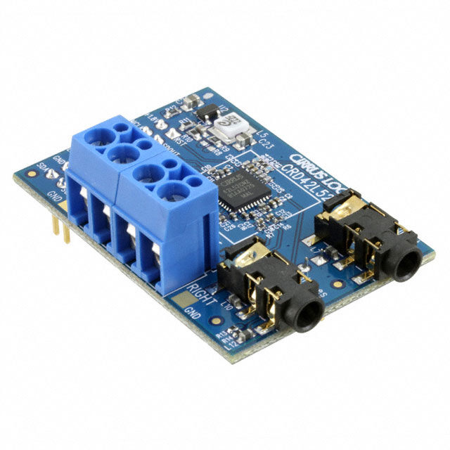
ICGOO电子元器件商城为您提供CRD42L52由Cirrus Logic设计生产,在icgoo商城现货销售,并且可以通过原厂、代理商等渠道进行代购。 CRD42L52价格参考。Cirrus LogicCRD42L52封装/规格:评估和演示板和套件, CS42L52 CODEC 音频 Evaluation Board。您可以下载CRD42L52参考资料、Datasheet数据手册功能说明书,资料中有CRD42L52 详细功能的应用电路图电压和使用方法及教程。
| 参数 | 数值 |
| 产品目录 | 编程器,开发系统 |
| 描述 | REFERENCE DESIGN FOR CS42L52 |
| 产品分类 | |
| 品牌 | Cirrus Logic Inc |
| 数据手册 | |
| 产品图片 | |
| 产品型号 | CRD42L52 |
| rohs | 含铅 / 不符合限制有害物质指令(RoHS)规范要求 |
| 产品系列 | - |
| 主要属性 | 2 个立体声模拟输入,立体声线路和耳机输出,S/PDIF 发射器和接收器 |
| 主要用途 | 音频编解码器 |
| 产品目录页面 | |
| 使用的IC/零件 | CS42L52 |
| 其它名称 | 598-1580 |
| 嵌入式 | 是,MCU,8 位 |
| 所含物品 | 板,软件 |
| 标准包装 | 1 |
| 相关产品 | /product-detail/zh/CS42L52-CNZR/CS42L52-CNZR-ND/2036663/product-detail/zh/CS42L52-CNZ/598-1628-ND/2024872 |
| 辅助属性 | 图形用户界面 |



- 商务部:美国ITC正式对集成电路等产品启动337调查
- 曝三星4nm工艺存在良率问题 高通将骁龙8 Gen1或转产台积电
- 太阳诱电将投资9.5亿元在常州建新厂生产MLCC 预计2023年完工
- 英特尔发布欧洲新工厂建设计划 深化IDM 2.0 战略
- 台积电先进制程称霸业界 有大客户加持明年业绩稳了
- 达到5530亿美元!SIA预计今年全球半导体销售额将创下新高
- 英特尔拟将自动驾驶子公司Mobileye上市 估值或超500亿美元
- 三星加码芯片和SET,合并消费电子和移动部门,撤换高东真等 CEO
- 三星电子宣布重大人事变动 还合并消费电子和移动部门
- 海关总署:前11个月进口集成电路产品价值2.52万亿元 增长14.8%


PDF Datasheet 数据手册内容提取
CRD42L52 Reference Design and Peripheral Driver Board for CS42L52 Reference Design Board (CRD42L52) Description Features In addition to providing a reference for an ultra small lay- out design, the purpose of the CRD42L52 is to allow a (cid:141) Ultra-Small Layout quick and easy evaluation of the CS42L52 low power (cid:141) Stake Header for External System Connections stereo CODEC. (cid:141) 1/8” Stereo Input Allows up to 2Vrms Signals Two 1/8” stereo jacks on the CRD42L52 provide an in- (cid:141) 1/8” Stereo Headphone Output Jack terface for analog line-level input and headphone-level (cid:141) Built-in Switch Control for CS42L52 SPKR/HP output connections to the CS42L52. Stereo differential Pin PWM speaker outputs from the CS42L52 can be moni- tored on a pair of screw terminals on the CRD42L52. (cid:141) Stereo Full Bridge Speaker Output Terminal The control port and serial audio interfaces are accessi- (cid:141) Complies with FCC class B and CISPR 22 ble via the I/O stake header used to attach the Standards for Radiated Emissions CRD42L52 to the CDB42LDB1. Peripheral Driver Board (CDB42LDB1) The CDB42LDB1 is a peripheral driver board that pro- Features vides clock/data, control logic and power supply to the CRD42L52. Digital data is transmitted and received via (cid:141) Multiple Power Supply Options S/PDIF optical and RCA connectors. The CRD42L52 – Three AAA Battery Source can be programmed by using the Windows Compatible FlexGUI software provided. Power is derived either – External Power Supply Header from three AAA batteries or from an external supply on (cid:141) S/PDIF I/O (CS8416 Receiver) the CDB42LDB1 driver board and is routed to the – Optical and RCA Input Jacks CRD42L52 via the I/O stake header. (cid:141) S/PDIF I/O (CS8406 Transmitter) – Optical and RCA Output Jacks ORDERING INFORMATION (cid:141) FlexGUI S/W Control - Windows® Compatible CRD42L52 Reference Design – Pre-Defined & User Configurable Scripts CDB42LDB1 Driver Board Speaker CRD42L52 Left USB + Line J3 External J4 Power - Input Microcontroller CS42L52 Right + AAA Battery Headphone Clip - Output I²C Control Port CPoI²noCtrrtol SAI SPuopwpelyr Micro Reset Interface PlacCeRhDol der Pushbutton I/O Header J5 S/PDIF Serial Audio Interface S/PDIF Input Output MCLK S/PDIF Rx 12.288 MHz S/PDIF Tx CS8416 CS8406 CDB42LDB1 Copyright © Cirrus Logic, Inc. 2008 APRIL '08 http://www.cirrus.com (All Rights Reserved) DS680RD1
CRD42L52 TABLE OF CONTENTS 1. SYSTEM OVERVIEW .............................................................................................................................4 1.1 Power (U2) .......................................................................................................................................4 1.2 Microcontroller (U3) .........................................................................................................................4 1.3 CS8416 Digital Audio Receiver (U7) ................................................................................................4 1.4 CS8406 Digital Audio Transmitter (U8) ............................................................................................4 1.5 Oscillator (Y1) ..................................................................................................................................5 1.6 CS42L52 Audio CODEC (U1) ..........................................................................................................5 1.7 Analog Input .....................................................................................................................................5 1.8 Analog Outputs ................................................................................................................................5 1.9 Layout ..............................................................................................................................................5 2. QUICK-START GUIDE ...........................................................................................................................6 3. CONFIGURATION OPTIONS .................................................................................................................7 3.1 S/PDIF In to Headphone Out ...........................................................................................................7 3.2 Line In to S/PDIF Out .......................................................................................................................7 3.3 S/PDIF In to Speaker Out ................................................................................................................8 3.4 Analog In to Analog Out - Digital Loopback .....................................................................................8 4. SOFTWARE MODE CONTROL .............................................................................................................9 4.1 CODEC Configuration Tab ............................................................................................................10 4.2 Analog Input Volume Tab ..............................................................................................................11 4.3 DSP Engine Tab ............................................................................................................................12 4.4 Analog and PWM Output Volume Tab ...........................................................................................13 4.5 Register Maps Tab .........................................................................................................................14 5. PERFORMANCE PLOTS .....................................................................................................................15 6. SYSTEM CONNECTIONS & INTERFACE ...........................................................................................18 CRD42L52 AND CDB42LDB1 BLOCK DIAGRAM ..............................................................................19 7. CRD42L52 SCHEMATICS ...................................................................................................................20 8. CDB42LDB1 SCHEMATICS ................................................................................................................21 9. CRD42L52 LAYOUT ............................................................................................................................23 10. CDB42LDB1 LAYOUT .......................................................................................................................24 11. REVISION HISTORY ..........................................................................................................................27 2 DS680RD1
CRD42L52 LIST OF FIGURES Figure 1.Quick-Start Guide .........................................................................................................................6 Figure 2.CRD42L52 and CDB42LDB1 Block Diagram for ADC and DAC Testing .....................................7 Figure 3.CRD42L52 and CDB42LDB1 Block Diagram for Digital Loopback Testing ..................................8 Figure 4.CODEC Configuration Tab .........................................................................................................10 Figure 5.Analog Input Volume Tab ...........................................................................................................11 Figure 6.DSP Engine Tab .........................................................................................................................12 Figure 7.Analog and PWM Output Volume Tab ........................................................................................13 Figure 8.Register Maps Tab ......................................................................................................................14 Figure 9.Dynamic Range - Line In to S/PDIF Out .....................................................................................15 Figure 10.Freq. Resp. - Line In to S/PDIF Out ..........................................................................................15 Figure 11.THD + N - Line In to S/PDIF Out ..............................................................................................15 Figure 12.FFT - S/PDIF In to HP Out @ 0 dBFS ......................................................................................15 Figure 13.FFT - S/PDIF In to HP Out @ -60 dBFS ...................................................................................16 Figure 14.Dynamic Range - S/PDIF In to HP Out .....................................................................................16 Figure 15.Freq. Resp. - S/PDIF In to HP Out ............................................................................................16 Figure 16.THD + N - S/PDIF In to HP Out ................................................................................................16 Figure 17.Freq. Resp. - S/PDIF In to Spkr. Out ........................................................................................16 Figure 18.Dynamic Range - Line In to HP Out (Dig. LB) ..........................................................................16 Figure 19.THD + N - Line In to HP Out (Dig. LB) ......................................................................................17 Figure 20.Block Diagram ...........................................................................................................................19 Figure 21.CS42L52 and Analog I/O ..........................................................................................................20 Figure 22.S/PDIF Input/Output ..................................................................................................................21 Figure 23.Microcontroller, Push Buttons and LED Indicators ...................................................................22 Figure 24.Silkscreen Top ..........................................................................................................................23 Figure 25.Silkscreen Bottom .....................................................................................................................23 Figure 26.Top-Side Layer .........................................................................................................................23 Figure 27.Internal Layer (Ground Plane) ..................................................................................................23 Figure 28.Internal Layer (Power Plane) ....................................................................................................23 Figure 29.Bottom-Side Layer ....................................................................................................................23 Figure 30.Silkscreen Top ..........................................................................................................................24 Figure 31.Silkscreen Bottom .....................................................................................................................24 Figure 32.Top-Side Layer .........................................................................................................................25 Figure 33.Layer 2 ......................................................................................................................................25 Figure 34.Layer 3 ......................................................................................................................................26 Figure 35.Bottom-Side Layer ....................................................................................................................26 LIST OF TABLES Table 1. S/PDIF In to Headphone Out Performance Plots ..........................................................................7 Table 2. Line In to S/PDIF Out Performance Plots .....................................................................................8 Table 3. S/PDIF In to Speaker Out Performance Plots ...............................................................................8 DS680RD1 3
CRD42L52 1. SYSTEM OVERVIEW The CRD42L52 provides a quick and general overview of the features in the CS42L52 CODEC in addition to pro- viding a reference for an ultra-small layout design. Line, headphone and PWM terminals are accommodated on the board for part evaluation and measurement pur- poses. The control port and serial audio interfaces are accessible via the I/O stake header used to attach the CRD42L52 to the CDB42LDB1. The driver board consists of a S/PDIF receiver, a S/PDIF transmitter and a USB microcontroller and is used to provide data to the CRD42L52. Therefore, in order to operate the CRD42L52 and use the Cirrus FlexGUI software to configure it, it must be connected to the CDB42LDB1 reference design board. This section serves to give a general overview of the hardware components used on the CRD42L52 reference design board and the CDB42LDB1 peripheral driver board. 1.1 Power (U2) Power can be supplied to the boards by using one of the two power supply options on the CDB42LDB1 driv- er board. Power is supplied to the driver board either from 3 AAA +1.5V batteries (placed on the battery clips behind the driver board) or from an external power supply (J1). The desired power supply must be se- lected using the appropriate setting on switch S1. The power supply on the driver board is regulated down to 3.3V and 1.8V as shown in the schematic (Figure 23 on page 22) to provide power to the various com- ponents on the driver board. The I/O header (J3) also contains power supply lines to route a 1.8V supply line to power the analog and digital cores of the CS42L52 on the CRD42L52 board. 1.2 Microcontroller (U3) The USB microcontroller on the CDB42LDB1 driver board drives the I²C® control port interface lines to the CRD42L52 via an I/O stake header and is used to configure the CS42L52. The microcontroller is also used to enable the CDB42LDB1 to drive the digital audio data and clock lines. On-board functionality can be controlled by selecting appropriate configuration settings in the provided Win- dows-compatible FlexGUI software. For a detailed description of the Cirrus FlexGUI software, refer to Sec- tion 4. "Software Mode Control". 1.3 CS8416 Digital Audio Receiver (U7) The CS8416 is a S/PDIF receiver that converts the S/PDIF data stream received by the board via either the optical or RCA phono connector into PCM data. This PCM data is routed to the I/O stake header which routes it to the CS42L52 on the CRD42L52 board. The CS8416 is configured to operate in hardware master mode and provides the system master clock when a S/PDIF input source is connected to the board. Should the S/PDIF source become unavailable, causing a Receiver Error, the system clock is automatically switched to the one provided by the on-board oscillator for uninterrupted operation of other on-board components receiving the master clock. A complete description of the CS8416 receiver and a discussion on the digital audio interface are included in the CS8416 data sheet. 1.4 CS8406 Digital Audio Transmitter (U8) The CS8406 is a S/PDIF transmitter that converts the PCM data it receives from the I/O stake header into a S/PDIF data stream. The S/PDIF data can be monitored either via the optical (J7) or RCA phono connector (J9) on the CDB42LDB1 driver board. The CS8406 is configured to operate in hardware slave mode. It re- ceives its clocks from the CS8416. In the case of a receiver error, the clock source for the CS8406 is auto- matically switched to the on-board oscillator for uninterrupted operation of the CS8406. A complete description of the CS8406 transmitter and a discussion on the digital audio interface are includ- ed in the CS8406 data sheet. 4 DS680RD1
CRD42L52 1.5 Oscillator (Y1) The on-board oscillator provides the system master clock when the digital audio receiver is powered down or when a receiver error occurs in the CS8416. Internal circuitry in the CS8416 automatically sets the oscil- lator clock as the new system clock whenever a receiver error is detected. This feature allows users to op- erate the boards without having a S/PDIF input fed to the board at all times. 1.6 CS42L52 Audio CODEC (U1) A complete description of the CS42L52 (Figure 21 on page 20) is included in the CS42L52 product data sheet. The CS42L52 is configured using the Windows-compatible Cirrus FlexGUI software provided. The I²C control port interface on the CS42L52 can be used for register manipulation and is controlled by the microcontroller on the CDB42LDB1 driver board. For full details on software functionality, refer to Section 4. "Software Mode Control". 1.7 Analog Input A 1/8” stereo jack can be used to supply stereo line-level analog inputs to the CS42L52 up to a full-scale value of 2Vrms. An AC-coupled passive filter and a voltage divider scale down the signal before sending it to the CS42L52 to prevent the signal from clipping. The CRD42L52 is routed to only allow analog inputs on input channel 1 of the CS42L52. Analog Input Chan- nels 2, 3 and 4 and Microphone Input Channels 1 and 2 are not connected. 1.8 Analog Outputs The analog output from the CS42L52’s ground-centered headphone amplifier can be monitored on the 1/8” stereo jack on the CRD42L52. Alternatively, one can also monitor the differential stereo PWM speaker out- put on the CS42L52 by using the differential speaker terminals J3 and J4. 1.9 Layout The CS42L52 requires only a minimal set of components to achieve specified performance results. Its inte- grated ground-centered amplifier eliminates the need for bulky DC-blocking capacitors and only requires two tiny ceramic capacitors for the charge pump. Additional components include load-stabilization circuitry and power supply decoupling. See the CS42L52 data sheet for further details. Figure 20 on page 19 provides an overview of the connections to the CS42L52. Figure 24 on page 23 and Figure 25 on page 23 show the component placement. Figure 26 on page 23 shows the top layout; Figure 27 on page 23 and Figure 28 on page 23 show the inner layers, and Figure 29 on page 23 shows the bottom layout. The decoupling capacitors are located as close to the CS42L52 as possible. Extensive use of ground plane fill in the reference design yields large reductions in radiated noise. DS680RD1 5
CRD42L52 2. QUICK-START GUIDE The following figure is supplied for user convenience as a simplified quick-start guide. Refer to Section 1 on page 4 and Section 3 on page 7 for details on how the various components on the board interface with each other in the different configuration modes. Refer to Section 4 on page 9 for descriptions on control settings in the Cirrus FlexGUI software. 6 5 i Connect Power supply Set switch to Place 3 AAA batteries with correct polarity on clips BT1, 5 ii between 1.6 V to 5 V. desired setting. BT2 and BT3 behind the board or perform step 5 ii. 7 Connect USB cable for communication between on-board microntroller and PC. Once connected, configure board using the FlexGUI software package provided. 2 3 Connect Connect either either S/PDIF S/PDIF optical optical or or BNC cables BNC cables for providing for receiving digital input. digital output. 4 Provide stereo analog line level input on stereo jack J7. 1 *Boards are not drawn Attach CRD42L52 to scale to driver board. 8 Monitor stereo headphone or differential speaker outputs. Figure 1. Quick-Start Guide 6 DS680RD1
CRD42L52 3. CONFIGURATION OPTIONS This section provides a deeper understanding of on-board circuitry and digital clock and data signal routing for ap- propriately setting the control software in a specific configuration. The section also provides the expected perfor- mance characteristics for the respective configuration mode. 12.288 MHz CRD42L52 CS42L52 Oscillator (SLAVE) AIN1A Serial CS8416 LineRT AIN1B EPnaobrtl e OMCK S/PDIF Rx SDOUT Input LRCLK SCLK R HP/ LINE_OUTB RMCK S/PDIF T HP/ LINE_OUTA (MASTER) IN Headphone Output CS8406 S/PDIF Tx SPKR_OUTB+ MCLK Right SPKR_OUTB- SCLK LRCLK SPKR_OUTA+ S/PDIF Left SDIN SPKR_OUTA- (SLAVE) OUT Figure 2. CRD42L52 and CDB42LDB1 Block Diagram for ADC and DAC Testing In order to test the ADC, DAC and PWM on the CS42L52, S/PDIF digital input needs to be provided to the CS8416 S/PDIF receiver on the CDB42LDB1 driver board via optical or RCA input jacks. The CS8416 operates in master mode and drives the serial audio interface lines to the CS42L52 and the CS8406, as shown in Figure2. For correct CS42L52 serial port operation, the CS42L52 serial port should be set up as a slave and the “Driver Board Serial Port” needs to be enabled in the FlexGUI software. 3.1 S/PDIF In to Headphone Out Stereo headphone-level analog outputs can be monitored on stereo jack J8 on the CRD42L52. Serial Audio digital clocks and data is routed to the CRD42L52 via I/O header J3. Table1 shows expected performance characteristics when the boards are configured to make digital input to analog output measurements. Plot Location FFT - S/PDIF In to Headphone Out @ 0 dBFS Figure 12 on page 15 FFT - S/PDIF In to Headphone Out @ -60 dB FS Figure 13 on page 16 Dynamic Range - S/PDIF In to Headphone Out Figure 14 on page 16 Frequency Response - S/PDIF In to Headphone Out Figure 15 on page 16 THD + N - S/PDIF In to Headphone Out Figure 16 on page 16 Table 1. S/PDIF In to Headphone Out Performance Plots 3.2 Line In to S/PDIF Out Line-level analog input can be provided to the CS42L52 via stereo jack J7 on the CRD42L52. The analog input path on the CRD42L52 scales the input down to a fifth of its actual value. Therefore, a 2.4Vrms analog input into the CRD42L52 is required to provide full-scale input to the CS42L52. The ADC core uses the clocks provided to the CS42L52 by the CS8416 to perform the conversion and outputs data to the CS8406 S/PDIF transmitter on the CDB42LDB1 driver board via the I/O header, J3. The S/PDIF output can be mon- itored on the RCA or optical jacks (J9 and J7). DS680RD1 7
CRD42L52 Table2 shows expected performance characteristics when the boards are configured to make analog input to digital output measurements. Plot Location Dynamic Range - Line In to S/PDIF Out Figure 9 on page 15 Frequency Response - Line In to S/PDIF Out Figure 10 on page 15 THD + N - Line In to S/PDIF Out Figure 11 on page 15 Table 2. Line In to S/PDIF Out Performance Plots 3.3 S/PDIF In to Speaker Out Stereo differential speaker outputs from the CS42L52 can be monitored on screw terminals J3 and J4. The CS42L52 can be set up to provide data to the PWM modulator for producing speaker outputs from either the serial port PCM input or the ADC output using the FlexGUI software. For a description of the Cirrus FlexGUI software controls, refer to Section 4 on page 9. Table3 shows expected performance characteris- tics when the boards are configured to make speaker output measurements. Plot Location Frequency Response - S/PDIF In to Speaker Out Figure 17 on page 16 Table 3. S/PDIF In to Speaker Out Performance Plots CRD42L52 CS42L52 (MASTER) AIN1A R LineT AIN1B 12.288 MHz Oscillator Input CS8416 RMCK S/PDIF Rx SDOUT LRCLK SCLK MCLK R HP/ LINE_OUTB (MASTER) T HP/ LINE_OUTA Headphone Output Figure 3. CRD42L52 and CDB42LDB1 Block Diagram for Digital Loopback Testing 3.4 Analog In to Analog Out - Digital Loopback In order to use the CS42L52 in digital loopback mode, one can configure the CS42L52 to operate in master or slave mode. Figure3 shows the board configuration when the CODEC is set up to operate in master mode. In this mode, the CS42L52 receives an MCLK from the driver board from the CS8416 S/PDIF reciev- er. As described in Section 1.3 on page 4 and shown in Figure3, the S/PDIF receiver uses the on-board 12.288 MHz clock as an MCLK when it is not receiving a S/PDIF input stream. Table3 shows expected per- formance characteristics when the boards are configured to make speaker output measurements. Plot Location Dynamic Range - Line In to HP Out (Digital Loopback) Figure 18 on page 16 THD + N - Line In to HP Out (Digital Loopback) Figure 19 on page 17 8 DS680RD1
CRD42L52 4. SOFTWARE MODE CONTROL The CRD42L52 may be used with the CDB42LDB1 driver board and the Microsoft® Windows-based FlexGUI graph- ical user interface, allowing software control of the CS42L52 and FPGA registers. The latest control software may be downloaded from www.cirrus.com/msasoftware. Step-by-step instructions for setting up the FlexGUI are pro- vided as follows: 1. Download and install the FlexGUI software as instructed on the Website. 2. Apply power using either an external source connected to screw terminal J1 or 3 AAA batteries (not includ- ed) on BT1, BT2 and BT3. 3. Connect the CDB42LDB1 to the host PC using a USB cable. 4. Launch the Cirrus FlexGUI. Once the GUI is launched successfully, all registers are set to their default reset state. 5. Refresh the GUI by clicking on the Update button. The default state of all registers are now visible. For standard set-up: 6. Set up the CS42L52 in the CODEC Configuration, Analog Input Volume Control, DSP Engine or Analog and PWM Output Volume Controls tab as desired. 7. Begin evaluating the CS42L52. For quick set-up, the CRD42L52 may, alternatively, be configured by loading a predefined sample script file: 8. On the File menu, click Restore Board Registers... 9. Browse to Boards\CRD42L52\Scripts\. 10. Choose any one of the provided scripts to begin evaluation. To create personal script files: 11. On the File menu, click Save Board Registers... 12. Enter any name that sufficiently describes the created setup. 13. Choose the desired location and save the script. 14. To load this script, follow the instructions from step 8 above. DS680RD1 9
CRD42L52 4.1 CODEC Configuration Tab The “CODEC Configuration” tab provides high-level control of various configurations for the CRD42L52. Status text detailing the CODEC’s specific configuration appears directly below the associated control. This text will change depending on the setting of the associated control. A description of each group is outlined below. See the CS42L52 data sheet for complete register descriptions. Power Control - Includes register controls for powering down the CODEC, ADC, PGA, headphone and speaker amplifiers. Microphone power register controls are not included as they are not connected on the CRD42L52 and are powered down by default. ADC Input Configuration - Includes controls for the internal PGA MUX and analog inputs. Serial Port Configuration - Includes controls for all settings related to the transmission and relationship of data and clocks within the CODEC. Driver Board Serial Port Disable - Controls the switch that allows the CDB42LDB1 to drive the data/clock I/O lines going to the CDB42LDB1 reference design board. Update - Reads all registers in the CS42L52 and reflects the current values in the GUI. Figure 4. CODEC Configuration Tab 10 DS680RD1
CRD42L52 4.2 Analog Input Volume Tab The “Analog Input Volume” tab provides high-level control of all volume settings in the ADC of the CS42L52. Status text detailing the CODEC’s specific configuration is shown inside the control group of the affected control. This text will change depending on the setting of the associated control. A description of each group is outlined below. See the CS42L52 data sheet for complete register descriptions. Digital Volume Control - Includes digital volume controls and adjustments for the ADC. ALC Configuration - Includes all configuration settings for the Automatic Level Control (ALC). Analog Volume Control - Includes all analog volume controls and adjustments for the PGA. Noise Gate Configuration - Includes all configuration settings for the noise gate. Update - Reads all registers in the CS42L52 and reflects the current values in the GUI. Reset - Resets the CS42L52. Figure 5. Analog Input Volume Tab DS680RD1 11
CRD42L52 4.3 DSP Engine Tab The “DSP Engine” tab provides high-level control of the SDIN (PCM) data volume level, the ADC out- put/SDIN mix volume level and the overall DAC/PWM channel volume level. DAC/PWM channel Limiter, Tone Control and Beep Generator control functions are also provided. Status text detailing the CODEC’s specific configuration is shown inside the control group of the affected control. This text will change depending on the setting of the associated control. A description of each group is outlined below. See the CS42L52 data sheet for complete register descriptions. Digital Volume Control - Digital volume controls and adjustments for the SDIN data, ADC out data and over- all channel volume. Mute, gang, invert and de-emphasis functions are also available. Limiter - Configuration settings for the Automatic Level Control (ALC). Tone Control - Bass and treble volume controls and filter corner frequencies. Beep Generator - On/Off time, frequency, volume, mix and repeat beep functions. Update - Reads all registers in the CS42L52 and reflects the current values in the GUI. Reset - Resets the CS42L52. Figure 6. DSP Engine Tab 12 DS680RD1
CRD42L52 4.4 Analog and PWM Output Volume Tab The “Analog and PWM Output Volume” tab provides high-level control of the CS42L52 input passthrough volume, HP/Line output volume levels, charge pump frequency, speaker volume, and PWM Tempera- ture/Battery monitoring controls. Status text detailing the CODEC’s specific configuration appears directly below the associated control. This text will change depending on the setting of the associated control. A description of each group is outlined below. See the CS42L52 data sheet for complete register descriptions. Headphone/Line Analog Output - Digital volume controls and adjustments for the DAC channel (outside of the DSP) and for the input passthrough. The modulation index and gain settings make up the parameters that determine the full scale headphone/line output level. PWM Output - Volume, mute, power down and other functional controls for the PWM speaker outputs. Temperature and Battery Monitor/Control - Battery Compensation, Thermal Foldback, Temperature Shut- down and Battery Monitor for the PWM/Speaker outputs. Figure 7. Analog and PWM Output Volume Tab DS680RD1 13
CRD42L52 4.5 Register Maps Tab The Advanced Register Debug tab provides low-level control of the CS42L52 individual register settings. Register values can be modified bit-wise or byte-wise. For bit-wise, click the appropriate push-button for the desired bit. For byte-wise, the desired hex value can be typed directly into the register address box in the register map. The “GPIO” tab may be ignored. Figure 8. Register Maps Tab 14 DS680RD1
CRD42L52 5. PERFORMANCE PLOTS Test conditions (unless otherwise specified): Input test signal is a full-scale 997 Hz sine wave; measurement band- width is 20Hz to 20kHz (unweighted); VA=VD=VA_HP=1.8V; Sample Frequency = 48kHz; HP test load: RL =10kΩ. -50 +5 -52.5 +4.5 -55 +4 -57.5 +3.5 -60 +3 -62.5 +2.5 -65 +2 -67.5 +1.5 -70 +1 d -72.5 d +0.5 BF -75 BF -0 S -77.5 S -0.5 -80 -1 -82.5 -1.5 -85 -2 -87.5 -2.5 -90 -3 -92.5 -3.5 -95 -4 -97.5 -4.5 -100 -5 20 50 100 200 500 1k 2k 5k 10k 20k 20 50 100 200 500 1k 2k 5k 10k 20k Hz Hz Figure 9. Dynamic Range - Line In to S/PDIF Out Figure 10. Freq. Resp. - Line In to S/PDIF Out -50 +0 -52.5 -10 -55 -57.5 -20 -60 -30 -62.5 * (Note 1) -65 -40 -67.5 -50 -70 d -72.5 d -60 BF -75 Br -70 S -77.5 A -80 -80 -82.5 -90 -85 -100 -87.5 -90 -110 -92.5 -120 -95 -97.5 -130 -10020 50 100 200 500 1k 2k 5k 10k 20k -14020 50 100 200 500 1k 2k 5k 10k 20k Hz Hz Figure 11. THD + N - Line In to S/PDIF Out Figure 12. FFT - S/PDIF In to HP Out @ 0 dBFS Notes: 1. The total harmonic distortion + noise (THD+N) performance of the ADC in the CS42L52 is determined by the value of the capacitor on the FILT+ pin. Larger capacitor values yield significant improvement in THD+N at low frequencies. A 1uF capacitor was used to make the performance measurement in Figure12. DS680RD1 15
CRD42L52 +0 -60 -10 -62.5 -65 -20 -67.5 -30 -70 -72.5 -40 -75 -50 -77.5 -80 -60 d d -82.5 B B r -70 r -85 A -80 A -87.5 -90 -90 -92.5 -100 -95 -97.5 -110 -100 -120 -102.5 -105 -130 -107.5 -14020 50 100 200 500 1k 2k 5k 10k 20k -11020 50 100 200 500 1k 2k 5k 10k 20k Hz Hz Figure 13. FFT - S/PDIF In to HP Out @ -60 dBFS Figure 14. Dynamic Range - S/PDIF In to HP Out +3 -60 +2.75 -62.5 +2.5 -65 +2.25 +2 -67.5 +1.75 -70 +1.5 -72.5 +1.25 -75 +1 -77.5 +0.75 +0.5 -80 Bd +0.25 Bd -82.5 r +0 r -85 A -0.25 A -87.5 -0.5 -90 -0.75 -1 -92.5 -1.25 -95 -1.5 -97.5 -1.75 -100 -2 -102.5 -2.25 -2.5 -105 -2.75 -107.5 -320 50 100 200 500 1k 2k 5k 10k 20k -11020 50 100 200 500 1k 2k 5k 10k 20k Hz Hz Figure 15. Freq. Resp. - S/PDIF In to HP Out Figure 16. THD + N - S/PDIF In to HP Out +5 -60 +4.5 -62 +4 -64 +3.5 -66 +3 -68 +2.5 -70 +2 -72 +1.5 -74 +1 -76 d +0.5 d -78 Br -0 Br -80 A -0.5 A -82 -1 -84 -1.5 -86 -2 -88 -2.5 -90 -3 -92 -3.5 -94 -4 -96 -4.5 -98 -520 50 100 200 500 1k 2k 5k 10k 20k -10020 50 100 200 500 1k 2k 5k 10k 20k Hz Hz Figure 17. Freq. Resp. - S/PDIF In to Spkr. Out Figure 18. Dynamic Range - Line In to HP Out (Dig. LB) 16 DS680RD1
CRD42L52 -60 -62 -64 *Note 1 -66 -68 -70 -72 d B -74 r -76 A -78 -80 -82 -84 -86 -88 -90 20 50 100 200 500 1k 2k 5k 10k 20k Hz Figure 19. THD + N - Line In to HP Out (Dig. LB) DS680RD1 17
CRD42L52 6. SYSTEM CONNECTIONS & INTERFACE On CDB42LDB1: Connector/ Reference Input/ Interface Designator Output Description BT1 AAA BT2 Input Battery Power Supply. BT3 Switch that selects which power supply is used by the CDB42LDB1 and the Power Supply Switch S1 Input CRD42L52. External Power J1 Input +5V - +2.7V external power supply. USB J2 Input/Output USB connection to PC for I²C control port signals. S/PDIF OPTICAL OUT J7 Output CS8406 digital audio output via optical cable. S/PDIF COAX OUT J9 Output CS8406 digital audio output via coaxial cable. S/PDIF OPTICAL IN J6 Input CS8416 digital audio input via optical cable. S/PDIF COAX IN J8 Input CS8416 digital audio input via coaxial cable. MICRO JTAG J5 Input/Output I/O for programming the micro controller (U3). MICRO RESET S4 Input Reset for the micro controller (U3). I/O routing between CDB42LDB1 and CRD42L52 containing Control Port I/O Header J3 Input/Output and Serial Audio Clock and Data . On CRD42L52: Connector/ Reference Input/ Interface Designator Output Description Line Input J7 Input Stereo jack for line level input signal to analog input channel 1 on CS42L52. Headphones J8 Output Stereo jack for monitoring stereo headphone output from CS42L52. SPEAKER LEFT J3 Screw Terminals for monitoring differential stereo speaker output from Output SPEAKER RIGHT J4 CS42L52. I/O routing between CDB42LDB1 and CRD42L52 containing Control Port I/O Header J5 Input/Output and Serial Audio Clock and Data . 18 DS680RD1
D CRD42L52 AND CDB42LDB1 BLOCK DIAGRAM S 6 8 0 R D 1 Speaker CRD42L52 Left USB + External Line J3 J4 Power - Input Microcontroller CS42L52 Right + AAA Battery Headphone Clip - Output I²C Control Port I²C Power Interface CRD Control SAI Supply Micro Reset Placeholder Port Pushbutton I/O Header J5 S/PDIF Serial Audio Interface S/PDIF Input Output MCLK S/PDIF Rx 12.288 MHz S/PDIF Tx CS8416 CS8406 CDB42LDB1 Figure 20. Block Diagram C R D 4 2 L 5 1 9 2
2 7. CRD42L52 SCHEMATICS 0 Figure 21. CS42L52 and Analog I/O C R D D S 4 6 8 2 0 L R D 5 1 2
D 8. CDB42LDB1 SCHEMATICS S 6 8 0 R D 1 C R D 4 2 Figure 22. S/PDIF Input/Output L 5 2 1 2
2 2 C R D D S 4 6 8 2 0 Figure 23. Microcontroller, Push Buttons and LED Indicators L R D 5 1 2
CRD42L52 9. CRD42L52 LAYOUT Figure 27. Internal Layer (Ground Plane) Figure 24. Silkscreen Top Figure 25. Silkscreen Bottom Figure 28. Internal Layer (Power Plane) Figure 26. Top-Side Layer Figure 29. Bottom-Side Layer DS680RD1 23
CRD42L52 10.CDB42LDB1 LAYOUT Figure 30. Silkscreen Top Figure 31. Silkscreen Bottom 24 DS680RD1
CRD42L52 Figure 32. Top-Side Layer Figure 33. Layer 2 DS680RD1 25
CRD42L52 Figure 34. Layer 3 Figure 35. Bottom-Side Layer 26 DS680RD1
CRD42L52 11.REVISION HISTORY Release Changes RD1 Initial Release DS680RD1 27
CRD42L52 Contacting Cirrus Logic Support For all product questions and inquiries, contact a Cirrus Logic Sales Representative. To find the one nearest you, go to www.cirrus.com. IMPORTANT NOTICE Cirrus Logic, Inc. and its subsidiaries (“Cirrus”) believe that the information contained in this document is accurate and reliable. However, the information is subject to change without notice and is provided “AS IS” without warranty of any kind (express or implied). Customers are advised to obtain the latest version of relevant information to verify, before placing orders, that information being relied on is current and complete. All products are sold subject to the terms and conditions of sale supplied at the time of order acknowledgment, including those pertaining to warranty, indemnification, and limitation of liability. No responsibility is assumed by Cirrus for the use of this information, including use of this information as the basis for manufacture or sale of any items, or for infringement of patents or other rights of third parties. This document is the property of Cirrus and by furnishing this information, Cirrus grants no license, express or implied under any patents, mask work rights, copyrights, trademarks, trade secrets or other intellectual property rights. Cirrus owns the copyrights associated with the information contained herein and gives con- sent for copies to be made of the information only for use within your organization with respect to Cirrus integrated circuits or other products of Cirrus. This consent does not extend to other copying such as copying for general distribution, advertising or promotional purposes, or for creating any work for resale. CERTAIN APPLICATIONS USING SEMICONDUCTOR PRODUCTS MAY INVOLVE POTENTIAL RISKS OF DEATH, PERSONAL INJURY, OR SEVERE PROP- ERTY OR ENVIRONMENTAL DAMAGE (“CRITICAL APPLICATIONS”). CIRRUS PRODUCTS ARE NOT DESIGNED, AUTHORIZED OR WARRANTED FOR USE IN PRODUCTS SURGICALLY IMPLANTED INTO THE BODY, AUTOMOTIVE SAFETY OR SECURITY DEVICES, LIFE SUPPORT PRODUCTS OR OTHER CRIT- ICAL APPLICATIONS. INCLUSION OF CIRRUS PRODUCTS IN SUCH APPLICATIONS IS UNDERSTOOD TO BE FULLY AT THE CUSTOMER’S RISK AND CIR- RUS DISCLAIMS AND MAKES NO WARRANTY, EXPRESS, STATUTORY OR IMPLIED, INCLUDING THE IMPLIED WARRANTIES OF MERCHANTABILITY AND FITNESS FOR PARTICULAR PURPOSE, WITH REGARD TO ANY CIRRUS PRODUCT THAT IS USED IN SUCH A MANNER. IF THE CUSTOMER OR CUSTOM- ER’S CUSTOMER USES OR PERMITS THE USE OF CIRRUS PRODUCTS IN CRITICAL APPLICATIONS, CUSTOMER AGREES, BY SUCH USE, TO FULLY INDEMNIFY CIRRUS, ITS OFFICERS, DIRECTORS, EMPLOYEES, DISTRIBUTORS AND OTHER AGENTS FROM ANY AND ALL LIABILITY, INCLUDING AT- TORNEYS’ FEES AND COSTS, THAT MAY RESULT FROM OR ARISE IN CONNECTION WITH THESE USES. Cirrus Logic, Cirrus, and the Cirrus Logic logo designs are trademarks of Cirrus Logic, Inc. All other brand and product names in this document may be trademarks or service marks of their respective owners. I²C is a registered trademark of Philips Semiconductor. Microsoft and Windows are registered trademarks of Microsoft Corporation. 28 DS680RD1
 Datasheet下载
