 Datasheet下载
- 型号: CP2130-F01-GM
- 制造商: Silicon Laboratories
- 库位|库存: xxxx|xxxx
- 要求:
| 数量阶梯 | 香港交货 | 国内含税 |
| +xxxx | $xxxx | ¥xxxx |
查看当月历史价格
查看今年历史价格
CP2130-F01-GM产品简介:
ICGOO电子元器件商城为您提供CP2130-F01-GM由Silicon Laboratories设计生产,在icgoo商城现货销售,并且可以通过原厂、代理商等渠道进行代购。 CP2130-F01-GM价格参考。Silicon LaboratoriesCP2130-F01-GM封装/规格:接口 - 控制器, USB 桥,USB 至 SPI USB 2.0 SPI 接口 24-QFN(4x4)。您可以下载CP2130-F01-GM参考资料、Datasheet数据手册功能说明书,资料中有CP2130-F01-GM 详细功能的应用电路图电压和使用方法及教程。
| 参数 | 数值 |
| 产品目录 | 集成电路 (IC)半导体 |
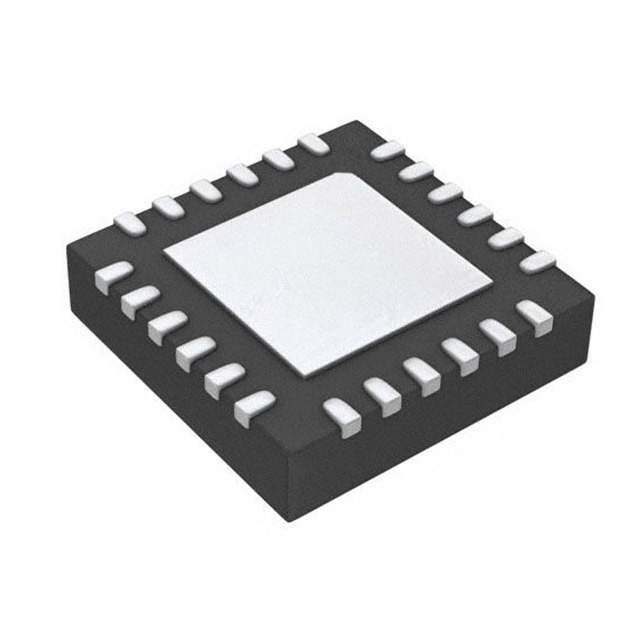
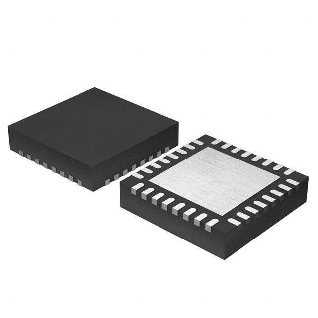
| 描述 | IC USB TO SPI BRIDGE 24QFN输入/输出控制器接口集成电路 USB to SPI bridge QFN24 |
| 产品分类 | |
| 品牌 | Silicon Laboratories IncSilicon Labs |
| 产品手册 | |
| 产品图片 |
|
| rohs | 符合RoHS无铅 / 符合限制有害物质指令(RoHS)规范要求 |
| 产品系列 | 接口 IC,输入/输出控制器接口集成电路,Silicon Labs CP2130-F01-GM- |
| 数据手册 | |
| 产品型号 | CP2130-F01-GMCP2130-F01-GM |
| USB修订版 | |
| 产品 | USB to SPI Bridge |
| 产品培训模块 | http://www.digikey.cn/PTM/IndividualPTM.page?site=cn&lang=zhs&ptm=30399 |
| 产品种类 | 输入/输出控制器接口集成电路 |
| 供应商器件封装 | 24-QFN(4x4) |
| 其它名称 | 336-2585 |
| 功能 | 桥,USB 至 UART |
| 包装 | 托盘 |
| 协议 | USB |
| 商标 | Silicon Labs |
| 安装风格 | SMD/SMT |
| 封装 | Tray |
| 封装/外壳 | 24-VFQFN 裸露焊盘 |
| 封装/箱体 | QFN-24 |
| 工作温度 | - |
| 工作电源电压 | 3.6 V |
| 工厂包装数量 | 91 |
| 接口 | UART |
| 接口类型 | SPI, USB |
| 最大工作温度 | + 85 C |
| 最小工作温度 | - 40 C |
| 标准 | USB 2.0 |
| 标准包装 | 91 |
| 特色产品 | http://www.digikey.cn/product-highlights/zh/cp2130-singlechip-usb/51256http://www.digikey.com/product-highlights/cn/zh/silicon-laboratories-the-internet-of-things/4179 |
| 电压-电源 | - |
| 电流-电源 | - |
| 电源电流 | 17.8 mA |
| 监视器 | No |
| 类型 | USB to SPI Bridge |
| 系列 | CP2130 |


- 商务部:美国ITC正式对集成电路等产品启动337调查
- 曝三星4nm工艺存在良率问题 高通将骁龙8 Gen1或转产台积电
- 太阳诱电将投资9.5亿元在常州建新厂生产MLCC 预计2023年完工
- 英特尔发布欧洲新工厂建设计划 深化IDM 2.0 战略
- 台积电先进制程称霸业界 有大客户加持明年业绩稳了
- 达到5530亿美元!SIA预计今年全球半导体销售额将创下新高
- 英特尔拟将自动驾驶子公司Mobileye上市 估值或超500亿美元
- 三星加码芯片和SET,合并消费电子和移动部门,撤换高东真等 CEO
- 三星电子宣布重大人事变动 还合并消费电子和移动部门
- 海关总署:前11个月进口集成电路产品价值2.52万亿元 增长14.8%


PDF Datasheet 数据手册内容提取
CP2130 SINGLE-CHIP USB-TO-SPI BRIDGE Single-Chip USB-to-SPI Bridge SPI Controller Integrated clock; no external crystal required 3 or 4-wire master mode operation Integrated USB transceiver; no external resistors Configurable clock rate required - 12MHz, 6MHz, 3MHz, 1.5MHz, 750kHz, 375kHz, Integrated 348 Byte one-time programmable ROM for 187.5kHz, 93.75kHz product customization Clock phase and polarity control On-chip power-on reset circuit Chip select mode and toggle On-chip voltage regulator: 3.45V output Programmable SPI delay (post-assert, inter-byte, pre- Uses USB Bulk Mode transactions for high throughput deassert) - Configurable priority for reads and writes 11 Configurable GPIO Pins with Alternate Functions USB Peripheral Function Controller Usable as inputs, open-drain outputs, or push-pull USB Specification 2.0 compliant; full-speed (12Mbps) outputs USB suspend states supported and indicated via Up to 11 chip select outputs suspend output pins Ready-to-read pin allows for external signal to trigger USB Interface SPI read operations Windows 8®, 7®, Vista®, and XP® Ability to count edges or pulses using the Event Counter Up to 11 USB remote wakeup sources Open access to interface specification SPI activity indication (toggles to indicate SPI activity) Windows Libraries Configurable clock output (93.75kHz to 24MHz) APIs for quick application development Supply Voltage Supports Windows 8®, 7®, Vista®, and XP® (SP2 & Self powered (regulator disabled): 3.0 to 3.6V SP3) Self powered (regulator enabled): 3.0 to 5.25V Packages USB bus powered: 4.0 to 5.25V RoHS-compliant 24-QFN package (4x4mm) I/O voltage: 1.8V to VDD Ordering Part Numbers CP2130-F01-GM Temperature Range: –40 to +85°C CP2130 Connect to VBUS VREGIN Voltage 48 MHz MISO To SPI or External Supply VDD Regulator Oscillator SPI Controller MOSI Slave SCK Devices USB GND Connector USB Interface Multi-Function VBUS VBUS Signals D+ D+ Full-Speed Peripheral GPIO GPIO.0_CS0 D- D- Tr1a2n sMcbepivse r CFounntcrotiollenr SPI Chip Select GPIO.1_CS1 GND GPIO.2_CS2 SPI ReadyToRead GPIO.3_CS3_RTR Multi- SPI Event Counter GPIO.4_CS4_EVTCNTR Function GPIO.5_CS5_CLKOUT Signals to Hardware Reset RESET 348 Byte PROM Clock Output GPIO.6_CS6 External GPIO.7_CS7 VPP SPI Activity Circuitry (Product Customization) GPIO.8_CS8_SPIACT USB Suspend GPIO.9_CS9_SUSPEND Logic Level Remote Wakeup GPIO.10_CS10_SUSPEND Supply VIO I/O Power and Logic Levels (1.8 V to VDD) Figure 1. Example System Diagram Rev. 0.7 1/14 Copyright © 2014 by Silicon Laboratories CP2130 This information applies to a product under development. Its characteristics and specifications are subject to change without notice.
CP2130 2 Rev. 0.7
CP2130 TABLE OF CONTENTS Section Page 1. System Overview . . . . . . . . . . . . . . . . . . . . . . . . . . . . . . . . . . . . . . . . . . . . . . . . . . . . . . . . .4 2. Electrical Characteristics . . . . . . . . . . . . . . . . . . . . . . . . . . . . . . . . . . . . . . . . . . . . . . . . . .5 3. USB Function Controller and Transceiver . . . . . . . . . . . . . . . . . . . . . . . . . . . . . . . . . . . . .9 4. Serial Peripheral Interface (SPI) . . . . . . . . . . . . . . . . . . . . . . . . . . . . . . . . . . . . . . . . . . . .10 4.1. Signal Descriptions . . . . . . . . . . . . . . . . . . . . . . . . . . . . . . . . . . . . . . . . . . . . . . . . . .10 4.2. Data Throughput . . . . . . . . . . . . . . . . . . . . . . . . . . . . . . . . . . . . . . . . . . . . . . . . . . . .11 4.3. Serial Clock Phase and Polarity . . . . . . . . . . . . . . . . . . . . . . . . . . . . . . . . . . . . . . . .11 5. GPIO Pins . . . . . . . . . . . . . . . . . . . . . . . . . . . . . . . . . . . . . . . . . . . . . . . . . . . . . . . . . . . . . .14 5.1. GPIO.3—Ready-to-Read (RTR) . . . . . . . . . . . . . . . . . . . . . . . . . . . . . . . . . . . . . . . .15 5.2. GPIO.4—Event Counter . . . . . . . . . . . . . . . . . . . . . . . . . . . . . . . . . . . . . . . . . . . . . .15 5.3. GPIO.5—Clock Output . . . . . . . . . . . . . . . . . . . . . . . . . . . . . . . . . . . . . . . . . . . . . . .15 5.4. GPIO.8—SPI Activity Indicator . . . . . . . . . . . . . . . . . . . . . . . . . . . . . . . . . . . . . . . . .16 5.5. GPIO.9-10—SUSPEND and SUSPEND . . . . . . . . . . . . . . . . . . . . . . . . . . . . . . . . . .16 5.6. USB Remote Wakeup . . . . . . . . . . . . . . . . . . . . . . . . . . . . . . . . . . . . . . . . . . . . . . . .16 5.7. GPIO State During USB Suspend . . . . . . . . . . . . . . . . . . . . . . . . . . . . . . . . . . . . . . .16 6. One-Time Programmable ROM . . . . . . . . . . . . . . . . . . . . . . . . . . . . . . . . . . . . . . . . . . . . .17 7. Voltage Regulator . . . . . . . . . . . . . . . . . . . . . . . . . . . . . . . . . . . . . . . . . . . . . . . . . . . . . . . .18 8. CP2130 Interface Specification and Windows Interface DLL . . . . . . . . . . . . . . . . . . . . .20 9. Relevant Application Notes . . . . . . . . . . . . . . . . . . . . . . . . . . . . . . . . . . . . . . . . . . . . . . . .20 10. Pin Descriptions . . . . . . . . . . . . . . . . . . . . . . . . . . . . . . . . . . . . . . . . . . . . . . . . . . . . . . . .21 11. QFN-24 Package Specifications . . . . . . . . . . . . . . . . . . . . . . . . . . . . . . . . . . . . . . . . . . .24 12. PCB Land Pattern . . . . . . . . . . . . . . . . . . . . . . . . . . . . . . . . . . . . . . . . . . . . . . . . . . . . . . .25 Document Change List . . . . . . . . . . . . . . . . . . . . . . . . . . . . . . . . . . . . . . . . . . . . . . . . . . . . .26 Contact Information . . . . . . . . . . . . . . . . . . . . . . . . . . . . . . . . . . . . . . . . . . . . . . . . . . . . . . . .27 Rev. 0.7 3
CP2130 1. System Overview The CP2130 is a highly-integrated USB-to-SPI bridge controller providing a simple solution for bridging a Universal Serial Bus (USB) host to a Serial Peripheral Interface (SPI) bus using a minimum of components and PCB space. The CP2130 includes a USB 2.0 full-speed controller, USB transceiver, oscillator, one-time programmable (OTP) ROM, and a SPI controller in a compact 4x4mm QFN24 package (sometimes called “MLF” or “MLP”). The on-chip, OTP ROM provides the option to customize the USB Vendor ID, Product ID, Manufacturer String, Product Description String, Power Descriptor, Device Release Number, Device Serial Number, and GPIO configuration as desired for OEM applications. The CP2130 uses a Silicon Labs vendor-specific USB protocol using control and bulk transfers which is supported by most operating systems through the use of generic USB drivers and interface libraries. A custom driver typically does not need to be developed for this device. Windows applications communicate with the CP2130 through a Windows DLL which is provided by Silicon Labs that communicates with the Microsoft WinUSB driver via a WinUSB DLL. The interface specification for the CP2130 is also available to enable development of an API for any operating system that supports control and bulk transfers over USB. The CP2130 SPI implements the standard signals, including SCK, MISO, MOSI, CS, as well as a ready-to-read (RTR) hardware handshaking input, so existing system firmware does not need to be modified. The SPI capabilities of the CP2130 include fixed SPI clock rates ranging from 93.75kHz to 12MHz, configurable clock phase, configurable clock polarity, adjustable SPI delays, and up to 11 configurable chip select signals. Any of the multi-purpose pins not used as chip select signals may instead be used as GPIO signals that are user- defined. The GPIO signals may also be configured to initiate a USB remote wakeup event on GPIO state change, which allows the CP2130 to wake a USB host from sleep mode. Eight of the GPIO signals support alternate features including ready-to-read (RTR) handshaking, a configurable event counter, a configurable clock output (93.75kHz to 24MHz), SPI activity LED toggle, and USB suspend indicators. Support for I/O interface voltages down to 1.8V is provided via a V pin. IO An evaluation kit for the CP2130 (Part Number: CP2130EK) is available. It includes a CP2130-based USB-to-SPI evaluation board with SPI slave devices such as an EEPROM and ADC as well as connections for an external CP2400 LCD controller EVB and SPI monitor. The kit also includes a Windows DLL and test application, USB cables, and full documentation. See www.silabs.com for the latest application notes and product support information for the CP2130. Contact a Silicon Labs sales representatives or go to www.silabs.com to order the CP2130 Evaluation Kit. 4 Rev. 0.7
CP2130 2. Electrical Characteristics Table 1. Global DC Electrical Characteristics V =3.0 to 3.6V, –40 to +85°C unless otherwise specified. DD Parameter Symbol Test Condition Min Typ Max Unit Digital Supply Voltage V 3.0 — 3.6 V DD Digital Port I/O Supply V 1.8 — V V IO DD Voltage Specified Operating T –40 — +85 °C A Temperature Range Thermal Resistance1 θ — 28 — °C/W JA Supply Current Bus Powered; Regulator enabled — 170 360 µA USB Suspended2 Self Powered; Regulator disabled; V =3.0V — 170 290 µA DD Self Powered; Regulator disabled; V =3.3V — 210 330 µA DD Bus Powered; Regulator enabled — 14.4 18.8 mA USB Normal; SPI Idle2 I Self Powered; Regulator disabled; V =3.0V — 13.8 18.1 mA REGIN DD Self Powered; Regulator disabled; V =3.3V — 14.1 18.4 mA DD Bus Powered; Regulator enabled — 17.8 23.2 mA USB Normal; SPI Self Powered; Regulator disabled; V =3.0V — 16.6 21.7 mA Active2 DD Self Powered; Regulator disabled; V =3.3V — 17.1 22.2 mA DD USB Pull-up3 I — 200 230 µA PU Notes: 1. Thermal resistance assumes a multi-layer PCB with any exposed pad soldered to a PCB pad. 2. USB Pull-up current should be added for total supply current. USB normal and suspended supply current is current flowing into V . USB normal and suspended supply current is guaranteed by characterization. REGIN 3. The USB Pull-up supply current values are calculated values based on USB specifications. USB Pull-up supply current is current flowing from VDD to GND through USB pull-down/pull-up resistors on D+ and D-. Rev. 0.7 5
CP2130 Table 2. SPI, Port I/O, and Suspend I/O DC Electrical Characteristics V =1.8 to 3.6V, –40 to +85°C unless otherwise specified. IO Parameters Symbol Test Condition Min Typ Max Unit Output High Voltage V I =–10µA, Port I/O push-pull V –0.1 — — OH OH IO I =–3mA, Port I/O push-pull V –0.2 — — V OH IO I =–10mA, Port I/O push-pull — V –0.4 — OH IO Output Low Voltage V I =10µA — — 0.1 OL OL I =8.5mA — — 0.4 V OL I =25mA — 0.6 — OL Input High Voltage V 0.7 x V — — V IH IO Input Low Voltage V — — 0.6 V IL Input Leakage Current I Weak Pull-Up On, V = 0V — 25 50 µA L IN Maximum Input Voltage Open drain, logic high (1) — — 5.8 V Table 3. Reset Electrical Characteristics –40 to +85°C unless otherwise specified. Parameter Symbol Test Condition Min Typ Max Unit V Ramp Time t Time to V ≥ 2.7 V — — 1 ms DD RMP DD RST Input High Voltage V 0.75 x V — — V IHRESET IO RST Input Low Voltage V — — 0.6 V ILRESET RST Low Time to t 15 — — µs RSTL Generate a System Reset Table 4. Voltage Regulator Electrical Specifications –40 to +85°C unless otherwise specified. Parameter Symbol Test Condition Min Typ Max Unit Input Voltage Range1 V Regulator Enabled V + V — 5.25 V REGIN DD DO Output Voltage2 V Output Current=1 to 100mA 3.3 3.45 3.6 V DDOUT VBUS Detection Input V 2.5 — — V BUSTH Threshold Dropout Voltage V 1mA ≤ I ≤ 100mA — 1 — mV/mA DO DD Bias Current — — 120 µA Notes: 1. Input range specified for regulation. When the internal regulator is not used, should be tied to V . DD 2. The maximum regulator supply current is 100mA. This includes the supply current of the CP2130. 6 Rev. 0.7
CP2130 Table 5. GPIO Output Specifications –40 to +85°C unless otherwise specified. Parameter Symbol Test Condition Min Typ Max Unit GPIO.5 Clock Output* F F =configured F x F F x Hz CLKOUT CLKOUT CLKOUT CLKOUT CLKOUT frequency 0.985 1.015 SPI Activity Toggle Rate F — 10 — Hz SPIACT *Note: The clock output frequency is configurable from 93.75kHz to 24MHz. Table 6. USB Transceiver Electrical Characteristics* V =3.0V to 3.6V, –40 to +85°C unless otherwise specified. DD Parameter Symbol Test Condition Min Typ Max Unit Transmitter Output High Voltage V 2.8 — — V OH Output Low Voltage V — — 0.8 V OL Output Crossover Point V 1.3 — 2.0 V CRS Output Impedance Z Driving High — 36 — DRV Driving Low — 36 — Pull-up Resistance R Full Speed (D+ Pull-up) 1.425 1.5 1.575 k PU Output Rise Time T Full Speed 4 — 20 ns R Output Fall Time T Full Speed 4 — 20 ns F Receiver Differential Input Sensitivity V | (D+) - (D-) | 0.2 — — V DI Differential Input Common V 0.8 — 2.5 V CM Mode Range Input Leakage Current I Pullups Disabled — <1.0 — µA L *Note: Refer to the USB Specification for timing diagrams and symbol definitions. Table 7. OTP ROM Electrical Characteristics –40 to +85°C unless otherwise specified. Parameter Symbol Test Condition Min Typ Max Unit Digital Port I/O Supply Voltage V 3.3 — V V IO DD During Programming Voltage on V with respect to GND during a V V > 3.3 V 5.75 — V + V PP PP IO IO programming operation 3.6 Capacitor on V for In-system Programming — 4.7 — µF PP Rev. 0.7 7
CP2130 Table 8. Thermal Characteristics Parameter Symbol Min Typ Max Unit Thermal Resistance* θ — 28 — °C/W JA *Note: Thermal resistance assumes a multi-layer PCB with any exposed pad soldered to a PCB pad. Table 9. Absolute Maximum Ratings* Parameter Symbol Test Condition Min Typ Max Unit Ambient Temperature under Bias T –55 — 125 °C BIAS Storage Temperature T –65 — 150 °C STG Voltage on RST, GPIO, or SPI Pins with V > 2.2V –0.3 — 5.8 V IO respect to GND V < 2.2V –0.3 — V + 3.6 IO IO Voltage on VBUS with respect to GND V V > 3.0 V –0.3 — 5.8 V BUS DD V not powered –0.3 — V + 3.6 DD DD Voltage on V or V with respect to GND V –0.3 — 4.2 V DD IO DD Maximum Total Current through V , — — 500 mA DD V , REGIN, and GND IO Maximum Output Current Sunk by RST or — — 100 mA any I/O pin *Note: Stresses above those listed may cause permanent damage to the device. This is a stress rating only, and functional operation of the devices at or exceeding the conditions in the operation listings of this specification is not implied. Exposure to maximum rating conditions for extended periods may affect device reliability. 8 Rev. 0.7
CP2130 3. USB Function Controller and Transceiver The Universal Serial Bus (USB) function controller in the CP2130 is a USB 2.0-compliant, full-speed device with integrated transceiver and on-chip matching and pullup resistors. The USB function controller manages all data transfers between the USB and the SPI bus as well as command requests generated by the USB host and commands for controlling the function of the SPI and GPIO pins. The USB Suspend and Resume modes are supported for power management of both the CP2130 device as well as external circuitry. The CP2130 enters Suspend mode when Suspend signaling is detected on the bus. Upon entering Suspend mode, the Suspend signals are asserted. The Suspend signals are also asserted after a CP2130 reset until device configuration and USB Enumeration is complete. SUSPEND is logic high when the device is in the Suspend state, and logic low when the device is in normal mode. The SUSPEND pin has the opposite logic value of the SUSPEND pin. The CP2130 exits Suspend mode when any of the following occur: Resume signaling is detected or generated, a USB Reset signal is detected, the configured GPIO wakeup sources do not match the configured latch value, or a device reset occurs. SUSPEND and SUSPEND are weakly pulled to VIO in a high impedance state during a CP2130 reset. If this behavior is undesirable, a strong pulldown (10k) can be used to ensure SUSPEND remains low during reset. The CP2130 can be configured to use any of the GPIO pins as a remote wakeup source. While suspended, if any of the pins configured as a wakeup source does not match the configured wakeup match value, then the CP2130 will send remote wakeup signaling to the USB host. If the host has configured the CP2130 to enable remote wakeup, then the host will send resume signaling to the CP2130 and the device will exit Suspend mode. The logic level and output mode (push-pull or open-drain) of various pins during USB Suspend is configurable in the OTP ROM. See Section 6 for more information. Rev. 0.7 9
CP2130 4. Serial Peripheral Interface (SPI) The CP2130 Serial Peripheral Interface (SPI) provides access to a flexible, full-duplex synchronous serial bus. The CP2130 can operate as a master device in both 3-wire or 4-wire modes, and supports multiple slaves. Any of the 11 GPIO pins may be configured as chip select master outputs to select multiple SPI slave devices. 4.1. Signal Descriptions The four signals used by SPI (MOSI, MISO, SCK, CS) are described below. 4.1.1. Master Out, Slave In (MOSI) The master-out, slave-in (MOSI) signal is an output from a master device and an input to slave devices. It is used to serially transfer data from the master to the slave. Data is transferred most-significant bit first. 4.1.2. Master In, Slave Out (MISO) The master-in, slave-out (MISO) signal is an output from a slave device and an input to the master device. It is used to serially transfer data from the slave to the master. Data is transferred most-significant bit first. 4.1.3. Serial Clock (SCK) The serial clock (SCK) signal is an output from the master device and an input to slave devices. It is used to synchronize the transfer of data between the master and slave on the MOSI and MISO lines. Since the CP2130 always acts as a SPI master, it always drives SCK. 4.1.4. Chip Select (CS0 - CS10) The CP2130 may be used to control up to 11 different SPI slave devices using GPIO pins configured in chip select output mode. Chip select signals are active low. See Figure2 and Figure3 for typical connection diagrams of the various operational modes. Master Device Slave Device SCK SCK MISO MISO MOSI MOSI Figure 2. 3-Wire Single Master and 3-Wire Single Slave Mode Connection Diagram Master Device Slave Device SCK SCK MISO MISO MOSI MOSI CS0 CS CS1 Slave Device SCK MISO MOSI CS Figure 3. 4-Wire Single Master Mode and 4-Wire Slave Mode Connection Diagram 10 Rev. 0.7
CP2130 4.2. Data Throughput SPI read and write data transfer throughput can be affected by many factors including USB host performance, host driver and PC application performance, SPI clock rate, and data transfer size. Also USB bulk transfers are limited by available bandwidth on the bus; increased traffic on the bus may decrease SPI throughput. Additionally, the CP2130 can be configured to operate in high-priority write or high-priority read mode. The priority mode is configured in the OTP ROM. The CP2130 has two independent USB endpoints used for bulk data transfers. The first endpoint is double buffered whereas the second endpoint is single buffered. Each endpoint is used for only a single direction. A USB IN transfer is data transferred from the device to the host. A USB OUT transfer is data transferred from the host to the device. More information about the USB interface can be found in application note, “AN792: CP2130 Interface Specification”. By default, the CP2130 is configured in high-priority write mode, in which the double-buffered endpoint is used for OUT transfers and the single-buffered endpoint is used for IN transfers. Conversely, when the CP2130 is configured in high-priority read mode, the double-buffered endpoint is used for IN transfers and the single-buffered endpoint is used for OUT transfers. Table10 below shows the CP2130 typical SPI throughput in high-priority write and high-priority read modes using a 64-bit PC. Table 10. Typical SPI Throughput Device Configuration Conditions Write Read WriteRead Units Throughput Throughput Throughput High-Priority Write Mode F =12MHz; 4.9 4.6 3.5 Mbps SCK Block Size=64KB High-Priority Read Mode 4.2 6.6 2.9 Mbps 4.3. Serial Clock Phase and Polarity Four combinations of serial clock phase and polarity can be selected using SPI control commands over the USB interface. The clock phase (CPHA) specifies which clock edge is used to latch the data. The clock polarity (CPOL) selects between an active-high or active-low clock. Both master and slave devices must be configured to use the same clock phase and polarity. The clock and data line relationships are shown in Figure4. The SPI clock field of the SPI control command controls the master mode serial clock frequency. The clock frequency is restricted to discrete values between 93.8kHz and 12MHz. SCK (CPHA=Leading Edge, CPOL=Active High) SCK (CPHA=Trailing Edge, CPOL=Active High) SCK (CPHA=Leading Edge, CPOL=Active Low) SCK (CPHA=Trailing Edge, CPOL=Active Low) MISO/MOSI MSB Bit 6 Bit 5 Bit 4 Bit 3 Bit 2 Bit 1 Bit 0 Figure 4. Data/Clock Timing Rev. 0.7 11
CP2130 SCK Shift Edge SCK* 1 / F SCK TMIS TMIH MISO MOSI * SCK is shown for CPOL = Active High. SCK is the opposite polarity for CPOL = Active Low. Figure 5. SPI Master Timing (CPHA=Leading Edge) SCK Shift Edge SCK* TMIS TMIH MISO MOSI * SCK is shown for CPOL = Active High. SCK is the opposite polarity for CPOL = Active Low. Figure 6. SPI Master Timing (CPHA=Trailing Edge) 12 Rev. 0.7
CP2130 CS T T POST‐ASSERT PRE‐DEASSERT SCK* T INTER‐BYTE DELAY MISO/MOSI MSB LSB MSB LSB * SCK is shown for CPOL = Active High. SCK is the opposite polarity for CPOL = Active Low. Figure 7. SPI Delays (CPHA = Leading Edge) CS T T POST‐ASSERT PRE‐DEASSERT SCK* T INTER‐BYTE DELAY MISO/MOSI MSB LSB MSB LSB * SCK is shown for CPOL = Active High. SCK is the opposite polarity for CPOL = Active Low. Figure 8. SPI Delays (CPHA = Trailing Edge) Table 11. SPI Timing Parameters1 Parameter Symbol Min Typ Max Units 12MHz 6MHz 3MHz 1.5MHz SCK Frequency F SCK 750kHz 375kHz 187.5kHz 93.75kHz MISO Valid to SCK Shift Edge T 41.15 — — ns MIS SCK Shift Edge to MISO Change T 0 — — ns MIH Post-Assert SPI Delay2 T N x 10 µs POST-ASSERT Inter-Byte SPI Delay2 T N x 10 µs INTER-BYTE Pre-Deassert SPI Delay2 T N x 10 µs PRE-DEASSERT Notes: 1. See Figures 5–8. 2. N=user-specified delay values, where {0 ≤ N ≤ 65535}. Rev. 0.7 13
CP2130 5. GPIO Pins The CP2130 supports 11 user-configurable GPIO pins. Each of these GPIO pins are usable as inputs, open-drain outputs, or push-pull outputs. Each GPIO pin may also be configured for use as SPI chip select signals for up to 11 different SPI slaves. Six of these GPIO pins also have alternate functions which are listed in Table12. More information regarding the configuration and usage of these pins is available in application note, “AN721: CP21xx Customization Guide” available on the Silicon Labs website. Table 12. GPIO Pin Alternate Functions GPIO Pin Alternate Function GPIO.3 Ready-to-Read (RTR) GPIO.4 Event Counter GPIO.5 Clock Output GPIO.8 SPI Activity GPIO.9 SUSPEND GPIO.10 SUSPEND The default configuration for all of the GPIO pins is provided in Table13. The configuration of the pins is one-time programmable for each device. See Section 6 for more information about programming the GPIO pin functionality. Table 13. GPIO Pin Default Configuration GPIO Pin Default Function GPIO Pin Default Function GPIO.0 CS0 (Push-Pull Output) GPIO.6 GPIO (Input) GPIO.1 CS1 (Push-Pull Output) GPIO.7 GPIO (Push-Pull Output) GPIO.2 CS2 (Push-Pull Output) GPIO.8 SPI Activity (Push-Pull Output) GPIO.3 RTR Active Low (Input) GPIO.9 SUSPEND (Push-Pull Output) GPIO.4 Event Counter Rising Edge (Input) GPIO.10 SUSPEND (Push-Pull Output) GPIO.5 Clock Output (Push-Pull Output) The difference between an open-drain output and a push-pull output is evident when the GPIO output is driven to logic high. A logic high, open-drain output pulls the pin to the V rail through an internal, pull-up resistor. A logic IO high, push-pull output directly drives the pin to the V voltage. Open-drain outputs are typically used when IO interfacing to logic at a higher voltage than the V pin. These pins can be safely pulled to the higher, external IO voltage through an external pull-up resistor. The maximum external pull-up voltage is 5V. The speed of reading and writing the GPIO pins is subject to the timing of the USB interface and host computer. GPIO pins configured as inputs or outputs are not recommended for real-time signaling. The following paragraphs describe the alternate functions available on the corresponding GPIO pin. 14 Rev. 0.7
CP2130 5.1. GPIO.3—Ready-to-Read (RTR) RTR, or Ready-to-Read, is a configurable active-low or active-high input to the CP2130 and is used by the SPI slave device to indicate to the CP2130 when to read. When performing a Read with RTR command, the CP2130 will only read SPI data when the RTR pin is asserted. By default, GPIO.3 is configured to operate as the RTR input pin. In addition to the GPIO OTP ROM configuration, the device must be configured to use RTR flow control to use this pin. Master Device Slave Device MISO MISO MOSI MOSI SCK SCK RTR RTR Figure 9. Hardware Flow Control Typical Connection Diagram 5.2. GPIO.4—Event Counter GPIO.4 is configurable as an event counter digital input pin. The event counter can be configured to count edges or pulses. The four configurable modes are: rising edge, falling edge, positive pulse, or negative pulse. Once configured for event counter mode, the CP2130 maintains a 16-bit counter that increments by ‘1’ whenever the specified edge or pulse is detected. The user may query the CP2130 to get the current event count. The event counter can be used to detect slave interrupt events by connecting the slave interrupt output pin to the CP2130 event counter pin. 5.3. GPIO.5—Clock Output GPIO.5 is configurable to output a configurable CMOS clock output. The clock output appears at the pin at the same time the device completes enumeration and exits USB Suspend mode. The clock output is removed from the pin when the device enters USB Suspend mode. The output frequency is configurable through the use of a divider and the accuracy is specified in Table5. When the divider is set to 0, the output frequency is 93.75kHz. For divider values between 1 and 255, the output frequency is determined by the formula: 24MHz GPIO.5 Clock Frequency = --------------------- Divider Equation1.GPIO.0 Clock Output Frequency Rev. 0.7 15
CP2130 5.4. GPIO.8—SPI Activity Indicator GPIO.8 is configurable as a SPI activity indicator pin. This pin is logic high when a device is not transferring data over the SPI, and toggles at a fixed rate as specified in Table5 when a data transfer is in progress. Typically, this pin is connected to an LED to indicate data transfer. V IO CP2130 GPIO.8 – SPI Activity Figure 10. SPI Activity Toggle Typical Connection Diagram 5.5. GPIO.9-10—SUSPEND and SUSPEND GPIO.9 and GPIO.10 are configurable as active-high SUSPEND and active-low SUSPEND pins. The SUSPEND pin is logic high when the device is in the suspended state and logic low when the device is in the active mode. The SUSPEND pin has the opposite logic value of the SUSPEND pin. 5.6. USB Remote Wakeup Any of the GPIO pins may be used to trigger a USB remote wakeup event. Before the CP2130 enters the Suspend state, the device may be configured to wakeup on a port mismatch event. When any of the pins specified in the wakeup mask do not match the pin logic value specified in the wakeup value, the CP2130 will wakeup and signal remote wakeup on the bus. The CP2130 will assert USB remote wakeup signaling for 10 to 15ms before the host may respond by resuming the CP2130. Any GPIO pin used for remote wakeup must be configured as an input during the Suspend state. GPIO pins are selected as wakeup pins using the Wakeup Match Mask. The Wakeup Match Value specifies the logic level of the wakeup pin. When the pin level does not match the value specified, the device will wakeup. The default Wakeup Match Mask and Wakeup Match Value are shown in Table15. 5.7. GPIO State During USB Suspend All GPIO pins support programmable suspend state mode and latch values. When the CP2130 enter USB Suspend mode and the Use Suspend Mode and Values option is set, the CP2130 will reconfigure the GPIO pins just prior to entering USB Suspend mode. When the CP2130 resumes from USB Suspend mode, the GPIO pins revert to the previous function configurations and modes. 16 Rev. 0.7
CP2130 6. One-Time Programmable ROM The CP2130 includes an internal, OTP ROM that may be used to customize the USB Vendor ID (VID), Product ID (PID), Manufacturer String, Product Description String, Power Descriptor, Device Release Number, Device Serial Number, GPIO configuration, Suspend Pins and Modes as desired for OEM applications. If the OTP ROM has not been customized, the default configuration data shown in Table14 and Table15 is used. Table 14. Default USB Configuration Data Name Value Vendor ID 0x10C4 Product ID 0x87A0 Power Descriptor (Attributes) 0x80 (Bus-powered) Power Descriptor (Max. Power) 0x32 (100 mA) Release Number 0x0100 (Release Version 01.00) Transfer Priority High Priority Write Manufacturer String “Silicon Laboratories” (62 ASCII characters maximum) Product Description String “CP2130 USB-to-SPI Bridge” (62 ASCII characters maximum) Serial String Unique 8 character ASCII string (30 ASCII characters maximum) Table 15. Default GPIO, UART, and Suspend Configuration Data Name Value Name Value GPIO.0 CS0 push-pull output Use Suspend Mode False and Values GPIO.1 CS1 push-pull output Suspend Mode 0x0000 (open-drain) GPIO.2 CS2 push-pull output Suspend Latch 0x0000 (logic low) GPIO.3 RTR active low Wakeup Match Mask 0x0000 (ignore all) GPIO.4 Event counter rising edge Wakeup Match Value 0x0000 (match value logic low) GPIO.5 Clock output Clock Divider 0 (93.75kHz) GPIO.6 GPIO input GPIO.7 GPIO push-pull output GPIO.8 SPI activity push-pull output GPIO.9 SUSPEND push-pull output GPIO.10 SUSPEND push-pull output While customization of the USB configuration data is optional, customizing the VID/PID combination is strongly recommended. A unique VID/PID will prevent the device from being recognized by any other manufacturer’s software application. A vendor ID can be obtained from www.usb.org or Silicon Labs can provide a free PID for the OEM product that can be used with the Silicon Labs VID at www.silabs.com/RequestPID. All CP2130 devices are pre-programmed with a unique serial number. It is important to have a unique serial string if it is possible for multiple CP2130 devices to be connected to the same PC. Application note, “AN792: CP2130 Interface Specification”, includes more information about the programmable values and their valid options. Note that certain items in the OTP ROM are programmed as a group and programming one of the items in the group prevents further programming of any of the other items in the group. The configuration data OTP ROM is programmable by Silicon Labs prior to shipment with the desired configuration information. It can also be programmed in-system over the USB interface if a 4.7µF capacitor is connected between the V pin and ground. No other circuitry should be connected to V during a programming operation, PP PP and V must remain at 3.3V or higher to successfully write to the configuration OTP ROM. IO Rev. 0.7 17
CP2130 7. Voltage Regulator The CP2130 includes an on-chip 5V to 3.45V voltage regulator. This allows the CP2130 to be configured as either a USB bus-powered device or a USB self-powered device. A typical connection diagram of the device in a bus- powered application using the regulator is shown in Figure11. When enabled, the voltage regulator output appears on the V pin and can be used to power external devices. See Table4 for the voltage regulator electrical DD characteristics. Note: By default, the CP2130 is configured for bus-powered operation. The CP2130 OTP configuration must be changed if the device will be operated in either of the self-powered modes. If the regulator is used to provide V in a self-powered application, use the same connections from Figure11, but DD connect REGIN to an on-board 5V supply, and disconnect it from the VBUS pin. In addition, if REGIN may be unpowered while VBUS is 5V, a resistor divider (or functionally equivalent circuit) shown in Note 6 of Figure12 is required to meet the absolute maximum voltage on VBUS specification in Table9. Note 4 VIO 4.7 kohm CP2130 Note 1 VIO RST SUSPEND Suspend 3.45 V Power VDD SUSPEND Signals 4.7 F 0.1 F VPP Note 5 4.7 F SCK REGIN MOSI 1 F 0.1 F MISO GPIO.0 / CS0 GND GPIO.1 / CS1 GPIO.2 / CS2 SPI USB VBUS VBUS GPIO.3 / CS3 / RTR and Connector D+ D+ GPIO.4 / CS4 / EVTCNTR GPIO Signals D- D- GPIO.5 / CS5 / CLKOUT GND GPIO.6 / CS6 Shield GPIO.7 / CS7 GPIO.8 / CS8 / SPIACT GPIO.9 / CS9 / SUSPEND 0.1 F1 Mohm0.1 F Note 2 Note 3 GPIO.10 / CS10 / SUSPEND Notes: 1. VIO can be connected directly to VDD or to a supply as low as 1.8 V to set the I/O interface voltage. 2. USB connector shield decoupling capacitors and resistor are not required, but can be added for noise immunity. 3. Avalanche transient voltage suppression diodes compatible with Full-speed USB should be added at the connector for ESD protection. Use Littelfuse p/n SP0503BAHT or equivalent. 4. An external pull-up is not required, but can be added for noise immunity. 5. If programming the configuration ROM via USB, add a 4.7 F capacitor between VPP and ground. During a programming operation, do not connect the VPP pin to other circuitry, and ensure that VIO is at least 3.3 V. Figure 11. Typical Bus-Powered Connection Diagram 18 Rev. 0.7
CP2130 Alternatively, if 3.0 to 3.6V power is supplied to the V pin, the CP2130 can function as a USB self-powered DD device with the voltage regulator bypassed. For this configuration, tie the REGIN input to V to bypass the voltage DD regulator. A typical connection diagram showing the device in a self-powered application with the regulator bypassed is shown in Figure12. The USB max power and power attributes descriptor must match the device power usage and configuration. See application note, “AN721: CP21xx Customization Guide”, for information on how to customize USB descriptors for the CP2130. CP2130 Note 1 VIO Note 4 VIO 3.3 V VDD Power 4.7 kohm 4.7 F 0.1 F RST SUSPEND Suspend SUSPEND Signals REGIN VPP Note 5 1 F 0.1 F 4.7 F GND SCK MOSI Note 6 MISO (Optional) 24 k GPIO.0 / CS0 VBUS GPIO.1 / CS1 47 k GPIO.2 / CS2 SPI USB VBUS GPIO.3 / CS3 / RTR and Connector D+ D+ GPIO.4 / CS4 / EVTCNTR GPIO Signals D- D- GPIO.5 / CS5 / CLKOUT GND GPIO.6 / CS6 / MMACK Shield GPIO.7 / CS7 / MMREQ GPIO.8 / CS8 / SPIACT GPIO.9 / CS9 / SUSPEND 0.1 F1 Mohm0.1 F Note 2 Note 3 GPIO.10 / CS10 / SUSPEND Notes: 1. VIO can be connected directly to VDD or to a supply as low as 1.8 V to set the I/O interface voltage. 2. USB connector shield decoupling capacitors and resistor are not required, but can be added for noise immunity. 3. Avalanche transient voltage suppression diodes compatible with Full-speed USB should be added at the connector for ESD protection. Use Littelfuse p/n SP0503BAHT or equivalent. 4. An external pull-up is not required, but can be added for noise immunity. 5. If programming the configuration ROM via USB, add a 4.7 F capacitor between VPP and ground. During a programming operation, do not connect the VPP pin to other circuitry, and ensure that VIO is at least 3.3 V. 6. For self-powered systems where VDD and VIO may be unpowered when VBUS is connected to 5 V, a resistor divider (or functionally-equivalent circuit) on VBUS is required to meet the absolute maximum voltage on VBUS specification in the Electrical Characteristics section. Figure 12. Typical Self-Powered Connection Diagram (Regulator Bypass) Rev. 0.7 19
CP2130 8. CP2130 Interface Specification and Windows Interface DLL The CP2130 is a Bulk Mode USB device and requires a generic USB driver such as Microsoft’s WinUSB driver or the open-source LibUSB driver. The CP2130 uses a vendor-specific interface protocol, and so the host application or library must comply with the CP2130 Interface Specification to communicate with the device. The low-level USB specification for the CP2130 is provided in application note, “AN792: CP2130 Interface Specification.” This document describes all of the basic functions for opening, reading from, writing to, and closing the device as well as the OTP ROM programming functions. Silicon Labs also provides an interface library that encapsulates the CP2130 interface and also adds higher level features such as read/write time-outs. This library is the recommended interface for the CP2130. The interface library is provided as a Windows DLL. Documentation for the interface library API is included in the installation package. AN792: CP2130 Interface Specification and the library are available in the CP2130EK CD as well as online at: www.silabs.com. 9. Relevant Application Notes The following application notes are applicable to the CP2130. The latest versions of these application notes and their accompanying software are available at http://www.silabs.com/products/Interface/Pages/interface-application-notes.aspx. AN721: CP21xx Device Customization Guide. This application note describes how to use the AN721 software, CP21xx Customization Utility, to configure the USB parameters on CP2130 devices. AN792: CP2130 Interface Specification. This application note describes how to interface to the CP2130 using the low-level, USB bulk and control mode Interface. 20 Rev. 0.7
CP2130 10. Pin Descriptions R T R 0 1 2 3 / S S S S C C C C 0 / 1 / 2 / 3 / O SI O. O. O. O. S O PI PI PI PI MI M G G G G 4 3 2 1 0 9 2 2 2 2 2 1 SCK 1 18 GPIO.4 / CS4 / EVTCNTR GND 2 17 GPIO.5 / CS5 / CLKOUT D+ 3 CP2130-GM 16 VPP Top View D- 4 15 GPIO.6 / CS6 VIO 5 14 GPIO.7 / CS7 GND (optional) VDD 6 13 GPIO.8 / CS8 / SPIACT 7 8 9 10 11 12 N S T C D D GI U S N/ N N B R E E E V P P R S S U U S S 0 / 9 / 1 S S C 10 / C O.9 / O. PI PI G G Figure 13. QFN-24 Pinout Diagram (Top View) Rev. 0.7 21
CP2130 Table 16. CP2130 Pin Definitions Pin # Name Type Description 1 SCK D Out SPI clock output 2 GND Ground. Must be tied to ground. 3 D+ D I/O USB D+ 4 D– D I/O USB D– 5 V Power In I/O Supply Voltage Input. IO 6 V Power In Power Supply Voltage Input. DD Power Out Voltage Regulator Output. See Section 7. 7 REGIN Power In 5V Regulator Input. This pin is the input to the on-chip voltage regulator. 8 VBUS D In VBUS Sense Input. This pin should be connected to the VBUS signal of a USB network. 9 RST D I/O Device Reset. Open-drain output of internal power-on reset or V monitor. An DD external source can initiate a system reset by driving this pin low for the time specified in Table3. 10* N/C No connect. This pin should be left unconnected or tied to V . IO 11* GPIO.10 D I/O In GPIO mode, this pin is a user-configurable input or output. CS10 D Out In chip select mode, this pin is a SPI chip select output. SUSPEND D Out In USB suspend mode, this pin is Low when in USB suspend mode. 12* GPIO.9 D I/O In GPIO mode, this pin is a user-configurable input or output. CS9 D Out In chip select mode, this pin is a SPI chip select output. SUSPEND D Out In USB suspend mode, this pin is High when in USB suspend mode. 13* GPIO.8 D I/O In GPIO mode, this pin is a user-configurable input or output. CS8 D Out In chip select mode, this pin is a SPI chip select output. SPIACT D Out In SPI activity mode, this pin toggles to indicate SPI activity. 14* GPIO.7 D I/O In GPIO mode, this pin is a user-configurable input or output. CS7 D Out In chip select mode, this pin is a SPI chip select output. 15* GPIO.6 D I/O In GPIO mode, this pin is a user-configurable input or output. CS6 D Out In chip select mode, this pin is a SPI chip select output. 16* V Special Connect a 4.7µF capacitor between this pin and ground to support OTP ROM PP programming via the USB interface. *Note: Pin can be left unconnected when not in use. 22 Rev. 0.7
CP2130 Table 16. CP2130 Pin Definitions (Continued) Pin # Name Type Description 17* GPIO.5 D I/O In GPIO mode, this pin is a user-configurable input or output. CS5 D Out In chip select mode, this pin is a SPI chip select output. CLKOUT D Out In clock output mode, this pin outputs a configurable frequency clock signal. 18* GPIO.4 D I/O In GPIO mode, this pin is a user-configurable input or output. CS4 D Out In chip select mode, this pin is a SPI chip select output. EVTCNTR D In In event counter mode, this pin is an event counter input. 19* GPIO.3 D I/O In GPIO mode, this pin is a user-configurable input or output. CS3 D Out In chip select mode, this pin is a SPI chip select output. RTR D In In Ready-to-Read mode, this pin is a SPI read flow control input. 20* GPIO.2 D I/O In GPIO mode, this pin is a user-configurable input or output. CS2 D Out In chip select mode, this pin is a SPI chip select output. 21* GPIO.1 D I/O In GPIO mode, this pin is a user-configurable input or output. CS1 D Out In chip select mode, this pin is a SPI chip select output. 22* GPIO.0 D I/O In GPIO mode, this pin is a user-configurable input or output. CS0 D Out In chip select mode, this pin is a SPI chip select output. 23 MOSI D Out SPI master output/slave input 24 MISO D In SPI master input/slave output *Note: Pin can be left unconnected when not in use. Rev. 0.7 23
CP2130 11. QFN-24 Package Specifications Figure 14. QFN-24 Package Drawing Table 17. QFN-24 Package Dimensions Dimension Min Typ Max Dimension Min Typ Max A 0.70 0.75 0.80 L 0.30 0.40 0.50 A1 0.00 0.02 0.05 L1 0.00 — 0.15 b 0.18 0.25 0.30 aaa — — 0.15 D 4.00 BSC. bbb — — 0.10 D2 2.55 2.70 2.80 ddd — — 0.05 e 0.50 BSC. eee — — 0.08 E 4.00 BSC. Z — 0.24 — E2 2.55 2.70 2.80 Y — 0.18 — Notes: 1. All dimensions shown are in millimeters (mm) unless otherwise noted. 2. Dimensioning and Tolerancing per ANSI Y14.5M-1994. 3. This drawing conforms to JEDEC Solid State Outline MO-220, variation WGGD except for custom features D2, E2, Z, Y, and L which are toleranced per supplier designation. 4. Recommended card reflow profile is per the JEDEC/IPC J-STD-020 specification for Small Body Components. 24 Rev. 0.7
CP2130 12. PCB Land Pattern Figure 15. QFN-24 Recommended PCB Land Pattern Table 18. QFN-24 PCB Land Pattern Dimensions Dimension Min Max Dimension Min Max C1 3.90 4.00 X2 2.70 2.80 C2 3.90 4.00 Y1 0.65 0.75 E 0.50 BSC Y2 2.70 2.80 X1 0.20 0.30 Notes: General 1. All dimensions shown are in millimeters (mm) unless otherwise noted. 2. This Land Pattern Design is based on the IPC-7351 guidelines. Solder Mask Design 3. All metal pads are to be non-solder mask defined (NSMD). Clearance between the solder mask and the metal pad is to be 60µm minimum, all the way around the pad. Stencil Design 4. A stainless steel, laser-cut and electro-polished stencil with trapezoidal walls should be used to assure good solder paste release. 5. The stencil thickness should be 0.125mm (5 mils). 6. The ratio of stencil aperture to land pad size should be 1:1 for all perimeter pads. 7. A 2x2 array of 1.10 x1.10mm openings on a 1.30mm pitch should be used for the center pad. Card Assembly 8. A No-Clean, Type-3 solder paste is recommended. 9. The recommended card reflow profile is per the JEDEC/IPC J-STD-020 specification for Small Body Components. Rev. 0.7 25
CP2130 DOCUMENT CHANGE LIST Revision 0.5 to Revision 0.6 Updated pin configuration functions for GPIO.6 and GPIO.7. Revision 0.6 to Revision 0.7 Moved VBUS to a separate row and updated the specification in Table9, “Absolute Maximum Ratings*,” on page8. Added VPP Voltage specification to Table7, “OTP ROM Electrical Characteristics,” on page7. Updated "7. Voltage Regulator" on page 18 to add absolute maximum voltage on VBUS requirements in self-powered systems. Updated measured throughput numbers in Table10, “Typical SPI Throughput,” on page11. 26 Rev. 0.7
Simplicity Studio One-click access to MCU and wireless tools, documentation, software, source code libraries & more. Available for Windows, Mac and Linux! IoT Portfolio SW/HW Quality Support and Community www.silabs.com/IoT www.silabs.com/simplicity www.silabs.com/quality community.silabs.com Disclaimer Silicon Labs intends to provide customers with the latest, accurate, and in-depth documentation of all peripherals and modules available for system and software implementers using or intending to use the Silicon Labs products. Characterization data, available modules and peripherals, memory sizes and memory addresses refer to each specific device, and "Typical" parameters provided can and do vary in different applications. Application examples described herein are for illustrative purposes only. Silicon Labs reserves the right to make changes without further notice and limitation to product information, specifications, and descriptions herein, and does not give warranties as to the accuracy or completeness of the included information. Silicon Labs shall have no liability for the consequences of use of the information supplied herein. This document does not imply or express copyright licenses granted hereunder to design or fabricate any integrated circuits. The products are not designed or authorized to be used within any Life Support System without the specific written consent of Silicon Labs. A "Life Support System" is any product or system intended to support or sustain life and/or health, which, if it fails, can be reasonably expected to result in significant personal injury or death. Silicon Labs products are not designed or authorized for military applications. Silicon Labs products shall under no circumstances be used in weapons of mass destruction including (but not limited to) nuclear, biological or chemical weapons, or missiles capable of delivering such weapons. Trademark Information Silicon Laboratories Inc.® , Silicon Laboratories®, Silicon Labs®, SiLabs® and the Silicon Labs logo®, Bluegiga®, Bluegiga Logo®, Clockbuilder®, CMEMS®, DSPLL®, EFM®, EFM32®, EFR, Ember®, Energy Micro, Energy Micro logo and combinations thereof, "the world’s most energy friendly microcontrollers", Ember®, EZLink®, EZRadio®, EZRadioPRO®, Gecko®, ISOmodem®, Precision32®, ProSLIC®, Simplicity Studio®, SiPHY®, Telegesis, the Telegesis Logo®, USBXpress® and others are trademarks or registered trademarks of Silicon Labs. ARM, CORTEX, Cortex-M3 and THUMB are trademarks or registered trademarks of ARM Holdings. Keil is a registered trademark of ARM Limited. All other products or brand names mentioned herein are trademarks of their respective holders. Silicon Laboratories Inc. 400 West Cesar Chavez Austin, TX 78701 USA http://www.silabs.com
Mouser Electronics Authorized Distributor Click to View Pricing, Inventory, Delivery & Lifecycle Information: S ilicon Laboratories: CP2130-F01-GM CP2130-F01-GMR