 Datasheet下载
- 型号: CM1242-07CP
- 制造商: ON Semiconductor
- 库位|库存: xxxx|xxxx
- 要求:
| 数量阶梯 | 香港交货 | 国内含税 |
| +xxxx | $xxxx | ¥xxxx |
查看当月历史价格
查看今年历史价格
CM1242-07CP产品简介:
ICGOO电子元器件商城为您提供CM1242-07CP由ON Semiconductor设计生产,在icgoo商城现货销售,并且可以通过原厂、代理商等渠道进行代购。 CM1242-07CP价格参考。ON SemiconductorCM1242-07CP封装/规格:TVS - 二极管, 。您可以下载CM1242-07CP参考资料、Datasheet数据手册功能说明书,资料中有CM1242-07CP 详细功能的应用电路图电压和使用方法及教程。
CM1242-07CP是ON Semiconductor(现为安森美半导体)生产的一款TVS(瞬态电压抑制器)二极管。这款器件主要用于保护电路免受瞬态过电压的损害,例如静电放电(ESD)、电快速瞬变脉冲群(EFT)和雷击等引起的电压尖峰。以下是其主要应用场景:

 1. 消费电子设备
   CM1242-07CP广泛应用于各种消费电子产品中,如智能手机、平板电脑、笔记本电脑、电视和其他家用电器。它能够有效保护这些设备中的敏感元件,如USB接口、HDMI端口、音频插孔等,防止因外部电压波动或静电放电导致的损坏。

 2. 通信设备
   在通信设备中,如路由器、调制解调器、交换机等,CM1242-07CP可以用于保护数据传输线和电源线,确保设备在面对瞬态电压时仍能正常工作。特别是在室外使用的通信设备中,雷击是一个常见的威胁,该器件可以有效减少雷击对设备的影响。

 3. 汽车电子
   汽车电子系统中存在大量的电气干扰源,如发动机启动、开关操作等。CM1242-07CP可以用于保护车载电子设备,如导航系统、娱乐系统、传感器和控制器等,确保这些设备在复杂的电磁环境中稳定运行。此外,它还可以用于保护CAN总线、LIN总线等通信接口。

 4. 工业自动化
   在工业自动化领域,CM1242-07CP可用于保护PLC(可编程逻辑控制器)、传感器、执行器等设备。这些设备通常需要在恶劣的工业环境中工作,可能会受到电机启动、电弧焊接等引起的瞬态电压冲击。通过使用CM1242-07CP,可以显著提高系统的可靠性和稳定性。

 5. 医疗设备
   医疗设备对可靠性和安全性要求极高,任何瞬态电压都可能导致设备故障,进而影响患者的健康。CM1242-07CP可以用于保护医疗设备中的关键组件,如心电图仪、超声波设备、监护仪等,确保设备在紧急情况下仍能正常工作。

总之,CM1242-07CP凭借其出色的瞬态电压抑制能力,广泛应用于多个领域的电路保护,确保设备在面对瞬态电压时的安全性和可靠性。
| 参数 | 数值 |
| 产品目录 | |
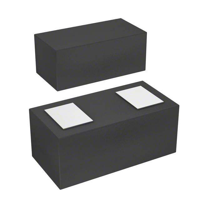
| 描述 | TVS DIODE 5VWM 9.8VC 2WLCSPESD 抑制器 1 CH. ESD PROTECTION |
| 产品分类 | |
| 品牌 | ON Semiconductor |
| 产品手册 | |
| 产品图片 |
|
| rohs | 符合RoHS无铅 / 符合限制有害物质指令(RoHS)规范要求 |
| 产品系列 | ON Semiconductor CM1242-07CP- |
| 数据手册 | |
| 产品型号 | CM1242-07CP |
| 不同频率时的电容 | - |
| 产品种类 | ESD 抑制器 |
| 供应商器件封装 | 2-WLCSP(0.6x0.3) |
| 其它名称 | CM1242-07CPOSDKR |
| 击穿电压 | 7.6 V |
| 功率-峰值脉冲 | - |
| 包装 | Digi-Reel® |
| 单向通道 | - |
| 双向通道 | 1 |
| 商标 | ON Semiconductor |
| 安装类型 | 表面贴装 |
| 封装 | Reel |
| 封装/外壳 | 2-XFBGA,WLCSP |
| 封装/箱体 | WLCSP-2 |
| 工作温度 | -40°C ~ 85°C (TA) |
| 工作温度范围 | - 40 C to + 85 C |
| 工厂包装数量 | 10000 |
| 应用 | 通用 |
| 标准包装 | 1 |
| 电压-击穿(最小值) | 6V |
| 电压-反向关态(典型值) | 5V |
| 电压-箝位(最大值)@Ipp | 9.8V (标准) |
| 电容 | 5.8 pF |
| 电流-峰值脉冲(10/1000µs) | 1A (8/20µs) |
| 电源线路保护 | 无 |
| 端接类型 | SMD/SMT |
| 类型 | 齐纳 |
| 系列 | CM1242-07 |
| 通道 | 1 Channel |


- 商务部:美国ITC正式对集成电路等产品启动337调查
- 曝三星4nm工艺存在良率问题 高通将骁龙8 Gen1或转产台积电
- 太阳诱电将投资9.5亿元在常州建新厂生产MLCC 预计2023年完工
- 英特尔发布欧洲新工厂建设计划 深化IDM 2.0 战略
- 台积电先进制程称霸业界 有大客户加持明年业绩稳了
- 达到5530亿美元!SIA预计今年全球半导体销售额将创下新高
- 英特尔拟将自动驾驶子公司Mobileye上市 估值或超500亿美元
- 三星加码芯片和SET,合并消费电子和移动部门,撤换高东真等 CEO
- 三星电子宣布重大人事变动 还合并消费电子和移动部门
- 海关总署:前11个月进口集成电路产品价值2.52万亿元 增长14.8%


PDF Datasheet 数据手册内容提取
CM1242-07CP 1-Channel Ultra Small 0201 Package ESD Protection Device in 0201 Description The CM1242−07CP is a 2−bump ESD protection device in 0201 http://onsemi.com form factor. It is fully compliant with IEC 61000−4−2. The CM1242−07CP is also RoHS II compliant and has a pure tin finish. Features • Low Capacitance < 5.8 pF WLCSP2 • CP SUFFIX Low Clamping Voltage CASE 567AV • Small Body Outline Dimensions:0.60 mm x 0.30 mm • Low Body Height: 0.275 mm • Stand−off Voltage: ±5.0 V BLOCK DIAGRAM • Low Dynamic Resistance: < 1.5 (cid:2) A • IEC61000−4−2 Level 4 ESD Protection • These Devices are Pb−Free, Halogen Free/BFR Free and are RoHS Compliant Table 1. PIN DESCRIPTIONS B Pin Description A ESD Channel Pin 1 MARKING DIAGRAM B ESD Channel Pin 2 PACKAGE / PINOUT DIAGRAMS A Top View (Bumps Down) A = Specific Device Code A ORDERING INFORMATION Device Package Shipping CM1242−07CP 10,000/Tape & Reel Bottom View (Pb−Free) (Bumps Up) †For information on tape and reel specifications, including part orientation and tape sizes, please refer to our Tape and Reel Packaging Specification Brochure, BRD8011/D. A B © Semiconductor Components Industries, LLC, 2012 1 Publication Order Number: July, 2012 − Rev. 5 CM1242−07CP/D
CM1242−07CP SPECIFICATIONS Table 2. STANDARD OPERATING CONDITIONS Parameter Rating Units Storage Temperature Range −55 to +150 °C Operating Temperature Range −40 to +85 °C Maximum Input Voltage ±5.5 V Table 3. ELECTRICAL OPERATING CHARACTERISTICS (Note 1) Symbol Parameter Conditions Min Typ Max Units VB Breakdown Voltage IF = +1.0 mA 6.0 7.6 9.0 V IF = −1.0 mA −9.0 −7.6 −6.0 ILEAK Channel Leakage Current VIN = ±5.0 V ±1.0 ±100 nA CIN Channel Input Capacitance At 1 MHz, VIN = 0 V 4.6 5.8 7.0 pF VESD ESD Protection Peak Discharge Voltage at any (Note 2) channel input kV a) Contact Discharge per IEC 61000−4−2 standard ±17 b) Air Discharge per IEC 61000−4−2 standard ±17 VCL Channel Clamp Voltage IPP = 1 A, tp = 8/20 (cid:3)s Positive Transients +9.8 V Negative Transients −9.8 RDYN Dynamic Resistance IPP = 1 A, tp = 8/20 (cid:3)s Positive Transients 1.5 (cid:2) Negative Transients 1.5 1. TA = 25°C unless otherwise specified. 2. Standard IEC 61000−4−2 with CDischarge = 150 pF, RDischarge = 330 (cid:2). Figure 1. ESD Clamping Voltage Screenshot Figure 2. ESD Clamping Voltage Screenshot Positive 8 kV Contact per IEC61000−4−2 Negative 8 kV Contact per IEC61000−4−2 http://onsemi.com 2
CM1242−07CP 20 1.00E−02 16 1.00E−03 12 1.00E−04 1.00E−05 8 1.00E−06 4 Ipk (A) −04 I1 (A)11..0000EE−−0078 1.00E−09 −8 1.00E−10 −12 CM1242 u1 1.00E−11 −16 CM1242 u2 1.00E−12 CM1242 u3 −20 1.00E−13 −32 −24 −16 −8 0 8 12 20 32 −9 −8−7 −6−5−4−3−2−1 0 1 2 3 4 5 6 7 8 9 Vpk (V) V1 (V) Figure 3. TLP Characteristics Figure 4. IV Characteristics 14 13 12 11 10 9 V) 8 k ( 7 p V 6 5 4 3 u1 2 u2 1 u3 0 0 0.5 1 1.5 2 2.5 3 3.5 Ipk (A) Figure 5. 80 x 20 Surge Characteristics Figure 6. Typical Insertion Loss (S21) http://onsemi.com 3
CM1242−07CP MECHANICAL SPECIFICATIONS CM1242−07CP Mechanical Specifications The CM1242−07CP is supplied in a 2−bump custom package. Dimensions are presented below. Table 4. TAPE AND REEL SPECIFICATIONS Pocket Size (mm) Tape Width Qty per Part Number Chip Size (mm) B0 X A0 X K0 W Reel Diameter Reel P0 P1 CM1242−07CP 0.60 X 0.30 X 0.275 0.67 X 0.37 X 0.35 8 mm 178 mm (7″) 10,000 4 mm 2 mm 10 Pitches Cumulative Tolerance P0 on Tape ±0.2 mm Top Cover Tape + + A0 K0 B0 W P1 User Direction of Feed Center Lines of Gravity Figure 7. Tape and Reel Mechanical Data CM1242−07CP Board Level Application. Refer to Application Note AND8398/D − Board Level Application Note for 0201 DSN2 Package. http://onsemi.com 4
CM1242−07CP PACKAGE DIMENSIONS WLCSP2, 0.6x0.3 CASE 567AV ISSUE O D A B NOTES: 1. DIMENSIONING AND TOLERANCING PER ASME Y14.5M, 1994. 2X 0.02 C 2. CONTROLLING DIMENSION: MILLIMETERS. MILLIMETERS DIM MIN MAX 2X 0.02 C E A 0.25 0.30 A1 0.00 0.05 TOP VIEW b 0.14 0.17 D 0.60 BSC E 0.30 BSC 0.02 C e 0.36 BSC A L 0.19 0.24 0.02 C A1 C SEATING SIDE VIEW PLANE RECOMMENDED e 2XL SOLDER FOOTPRINT* 2X 0.33 2Xb 0.05 C A B BOTTOM VIEW 2X 0.28 0.81 DIMENSIONS: MILLIMETERS *For additional information on our Pb−Free strategy and soldering details, please download the ON Semiconductor Soldering and Mounting Techniques Reference Manual, SOLDERRM/D. ON Semiconductor and are registered trademarks of Semiconductor Components Industries, LLC (SCILLC). SCILLC owns the rights to a number of patents, trademarks, copyrights, trade secrets, and other intellectual property. A listing of SCILLC’s product/patent coverage may be accessed at www.onsemi.com/site/pdf/Patent−Marking.pdf. SCILLC reserves the right to make changes without further notice to any products herein. SCILLC makes no warranty, representation or guarantee regarding the suitability of its products for any particular purpose, nor does SCILLC assume any liability arising out of the application or use of any product or circuit, and specifically disclaims any and all liability, including without limitation special, consequential or incidental damages. “Typical” parameters which may be provided in SCILLC data sheets and/or specifications can and do vary in different applications and actual performance may vary over time. All operating parameters, including “Typicals” must be validated for each customer application by customer’s technical experts. SCILLC does not convey any license under its patent rights nor the rights of others. SCILLC products are not designed, intended, or authorized for use as components in systems intended for surgical implant into the body, or other applications intended to support or sustain life, or for any other application in which the failure of the SCILLC product could create a situation where personal injury or death may occur. Should Buyer purchase or use SCILLC products for any such unintended or unauthorized application, Buyer shall indemnify and hold SCILLC and its officers, employees, subsidiaries, affiliates, and distributors harmless against all claims, costs, damages, and expenses, and reasonable attorney fees arising out of, directly or indirectly, any claim of personal injury or death associated with such unintended or unauthorized use, even if such claim alleges that SCILLC was negligent regarding the design or manufacture of the part. SCILLC is an Equal Opportunity/Affirmative Action Employer. This literature is subject to all applicable copyright laws and is not for resale in any manner. PUBLICATION ORDERING INFORMATION LITERATURE FULFILLMENT: N. American Technical Support: 800−282−9855 Toll Free ON Semiconductor Website: www.onsemi.com Literature Distribution Center for ON Semiconductor USA/Canada P.O. Box 5163, Denver, Colorado 80217 USA Europe, Middle East and Africa Technical Support: Order Literature: http://www.onsemi.com/orderlit Phone: 303−675−2175 or 800−344−3860 Toll Free USA/Canada Phone: 421 33 790 2910 Fax: 303−675−2176 or 800−344−3867 Toll Free USA/Canada Japan Customer Focus Center For additional information, please contact your local Email: orderlit@onsemi.com Phone: 81−3−5817−1050 Sales Representative http://onsemi.com CM1242−07CP/D 5
Mouser Electronics Authorized Distributor Click to View Pricing, Inventory, Delivery & Lifecycle Information: O N Semiconductor: CM1242-07CP