ICGOO在线商城 > 集成电路(IC) > 时钟/计时 - 时钟发生器,PLL,频率合成器 > CDCM9102RHBR
 Datasheet下载
- 型号: CDCM9102RHBR
- 制造商: Texas Instruments
- 库位|库存: xxxx|xxxx
- 要求:
| 数量阶梯 | 香港交货 | 国内含税 |
| +xxxx | $xxxx | ¥xxxx |
查看当月历史价格
查看今年历史价格
CDCM9102RHBR产品简介:
ICGOO电子元器件商城为您提供CDCM9102RHBR由Texas Instruments设计生产,在icgoo商城现货销售,并且可以通过原厂、代理商等渠道进行代购。 CDCM9102RHBR价格参考。Texas InstrumentsCDCM9102RHBR封装/规格:时钟/计时 - 时钟发生器,PLL,频率合成器, 。您可以下载CDCM9102RHBR参考资料、Datasheet数据手册功能说明书,资料中有CDCM9102RHBR 详细功能的应用电路图电压和使用方法及教程。
Texas Instruments(德州仪器)的CDCM9102RHBR是一款时钟发生器,属于时钟/计时类别中的PLL(锁相环)和频率合成器产品。它具有多种应用场景,尤其是在需要高精度、低抖动时钟信号的通信、网络设备、数据传输系统及高性能计算平台中。

 应用场景:

1. 通信设备:
   - CDCM9102RHBR适用于各种通信设备,如路由器、交换机、基站等。这些设备需要精确的时钟信号来确保数据同步和传输的稳定性。该器件能够生成多个输出频率,并且支持低抖动特性,从而保证通信系统的可靠性和高效性。

2. 网络基础设施:
   - 在数据中心、服务器集群和云计算环境中,CDCM9102RHBR可以为网络接口卡(NIC)、存储区域网络(SAN)和其他关键组件提供稳定的时钟源。其高精度和灵活性使得它成为构建可靠网络基础设施的理想选择。

3. 无线接入点与客户端设备:
   - 无论是Wi-Fi路由器还是物联网(IoT)终端设备,都需要一个稳定的时钟源以确保无线连接的质量。CDCM9102RHBR能够在这些应用中提供所需的时钟信号,支持多频段操作并保持良好的性能。

4. 测试与测量仪器:
   - 测试设备如示波器、频谱分析仪等对时钟精度要求极高。CDCM9102RHBR凭借其出色的抖动性能和宽泛的工作温度范围,非常适合用于这类专业仪器中,确保测量结果的准确性。

5. 消费电子与嵌入式系统:
   - 在某些高端音频设备、视频处理单元或工业控制系统中,CDCM9102RHBR也可以发挥重要作用,提供稳定可靠的时钟信号,以满足不同应用场景下的需求。

总之,CDCM9102RHBR凭借其卓越的性能和广泛的适用性,在众多领域中都展现出极高的价值,特别是在对时钟精度和稳定性有严格要求的应用场合。
| 参数 | 数值 |
| 产品目录 | 集成电路 (IC) |
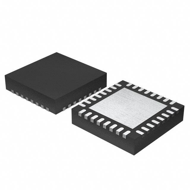
| 描述 | IC CLK GEN 100MHZ 32QFN |
| 产品分类 | |
| 品牌 | Texas Instruments |
| 数据手册 | |
| 产品图片 |
|
| 产品型号 | CDCM9102RHBR |
| PCN设计/规格 | |
| PLL | 无 |
| rohs | 无铅 / 符合限制有害物质指令(RoHS)规范要求 |
| 产品系列 | - |
| 供应商器件封装 | 32-VQFN(5x5) |
| 其它名称 | 296-30478-6 |
| 分频器/倍频器 | 无/无 |
| 包装 | Digi-Reel® |
| 安装类型 | 表面贴装 |
| 封装/外壳 | 32-VFQFN 裸露焊盘 |
| 工作温度 | -40°C ~ 85°C |
| 差分-输入:输出 | 无/是 |
| 标准包装 | 1 |
| 比率-输入:输出 | 1:3 |
| 电压-电源 | 3 V ~ 3.6 V |
| 电路数 | 1 |
| 类型 | 时钟发生器 |
| 输入 | |
| 输出 | LVCMOS,LVDS,LVPECL |
| 频率-最大值 | 100MHz |


PDF Datasheet 数据手册内容提取
Product Sample & Technical Tools & Support & Reference Folder Buy Documents Software Community Design CDCM9102 SCAS922A–FEBRUARY2012–REVISEDAPRIL2016 CDCM9102 Low-Noise Two-Channel 100-MHz Clock Generator 1 Features 3 Description • IntegratedLow-NoiseClockGeneratorIncluding The CDCM9102 is a low-jitter clock generator 1 designed to provide reference clocks for PLL,VCO,andLoopFilter communications standards such as PCI Express™. • TwoLow-Noise100-MHzClocks(LVPECL, The device supports up to PCIE gen3 and is easy to LVDS,orpairofLVCMOS) configure and use. The CDCM9102 provides two – SupportforHCSLSignalingLevels 100-MHz differential clock ports. The output types (AC-Coupled) supported for these ports include LVPECL, LVDS, or a pair of LVCMOS buffers. HCSL signaling is – TypicalPeriodJitter:21pspk-pk supported using an AC-coupled network. The user – TypicalRandomJitter:510fsRMS configures the output buffer type desired by strapping – OutputTypeSetbyPins device pins. Additionally, a single-ended 25-MHz clock output port is provided. Uses for this port • BonusSingle-Ended25-MHzOutput include general-purpose clocking, clocking Ethernet • IntegratedCrystalOscillatorInputAccepts PHYs, or providing a reference clock for additional 25-MHzCrystal clock generators. All clocks generated are derived • OutputEnablePinShutsOffDeviceandOutputs fromasingleexternal25-MHzcrystal. • 5-mm×5-mm32-PinVQFNPackage DeviceInformation(1) • ESDProtectionExceeds2000VHBM,500V PARTNUMBER PACKAGE BODYSIZE(NOM) CDM CDCM9102 VQFN(32) 5.00mm×5.00mm • IndustrialTemperatureRange(–40°Cto85°C) (1) For all available packages, see the orderable addendum at • 3.3-VPowerSupply theendofthedatasheet. 2 Applications • ReferenceClockGenerationforPCIExpress Gen1,Gen2,andGen3 • General-PurposeClocking SimplifiedSchematic VDD OUT1P HCSL input ITTP OUT1N OUT2P HCSL output OTTP OUT2N VDD OUT3P LP OUT3N Up to 8x 8 471 (cid:159)(cid:3) 471 (cid:159)(cid:3) 20 OUT4P 100MHz 100MHz LVPECL N1 OUT4N U IN1P C HCSL 25MHz CDCM9102 IN1N CD outputs 150 (cid:159)(cid:3) 150 (cid:159)(cid:3) 56 (cid:159)(cid:3) 56 (cid:159)(cid:3) OUT8P OUT8N Copyright © 2016, Texas Instruments Incorporated 1 An IMPORTANT NOTICE at the end of this data sheet addresses availability, warranty, changes, use in safety-critical applications, intellectualpropertymattersandotherimportantdisclaimers.PRODUCTIONDATA.
CDCM9102 SCAS922A–FEBRUARY2012–REVISEDAPRIL2016 www.ti.com Table of Contents 1 Features.................................................................. 1 9.3 FeatureDescription.................................................10 2 Applications........................................................... 1 9.4 DeviceFunctionalModes.......................................10 3 Description............................................................. 1 9.5 Programming...........................................................12 4 RevisionHistory..................................................... 2 10 ApplicationandImplementation........................ 13 10.1 ApplicationInformation..........................................13 5 DeviceComparisonTable..................................... 3 10.2 TypicalApplication................................................16 6 PinConfigurationandFunctions......................... 3 11 PowerSupplyRecommendations..................... 19 7 Specifications......................................................... 5 11.1 ThermalManagement...........................................19 7.1 AbsoluteMaximumRatings......................................5 11.2 PowerSupplyFiltering..........................................19 7.2 ESDRatings..............................................................5 12 Layout................................................................... 20 7.3 RecommendedOperatingConditions.......................5 12.1 LayoutGuidelines.................................................20 7.4 ThermalInformation..................................................5 12.2 LayoutExample....................................................20 7.5 ElectricalCharacteristics...........................................6 13 DeviceandDocumentationSupport................. 21 7.6 TimingRequirements................................................7 7.7 TypicalCharacteristics..............................................7 13.1 CommunityResources..........................................21 13.2 Trademarks...........................................................21 8 ParameterMeasurementInformation..................8 13.3 ElectrostaticDischargeCaution............................21 8.1 TestConfigurations...................................................8 13.4 Glossary................................................................21 9 DetailedDescription............................................ 10 14 Mechanical,Packaging,andOrderable 9.1 Overview.................................................................10 Information........................................................... 21 9.2 FunctionalBlockDiagrams.....................................10 4 Revision History NOTE:Pagenumbersforpreviousrevisionsmaydifferfrompagenumbersinthecurrentversion. ChangesfromOriginal(February2012)toRevisionA Page • AddedESDRatingstable,FeatureDescriptionsection,DeviceFunctionalModes,ApplicationandImplementation section,PowerSupplyRecommendationssection,Layoutsection,DeviceandDocumentationSupportsection,and Mechanical,Packaging,andOrderableInformationsection.................................................................................................. 1 • AddedtexttoDescription:ThedevicesupportsuptoPCIEgen3andis.............................................................................. 1 • Changedpartnumberto113425M0000000....................................................................................................................... 11 • ChangedpartnumbertoFP2500002................................................................................................................................... 11 • AddedtextandFigure16toPCIExpressApplications....................................................................................................... 15 2 SubmitDocumentationFeedback Copyright©2012–2016,TexasInstrumentsIncorporated ProductFolderLinks:CDCM9102
CDCM9102 www.ti.com SCAS922A–FEBRUARY2012–REVISEDAPRIL2016 5 Device Comparison Table PACKAGEDDEVICES FEATURES T A CDCM9102RHBT 32-pinVQFN(RHB)package,smalltapeandreel –40°Cto85°C CDCM9102RHBR 32-pinVQFN(RHB)package,tapeandreel 6 Pin Configuration and Functions RHBPackage 32-PinVQFN (TopView) 1 2 T P P U A A O 6 C 5 C C D D G D G C S N N D E D E N O G XI V R V R 4 3 2 1 0 9 8 7 2 2 2 2 2 1 1 1 NC 25 16 VDD4 NC 26 15 NC NC 27 14 GND NC 28 13 NC GND NC 29 12 RESET NC 30 11 OS0 NC 31 10 OS1 NC 32 9 VDD3 1 2 3 4 5 6 7 8 2 N P 1 N P E C D 1 1 D 0 0 O N D T T D T T V U U V U U O O O O PinFunctions PIN TYPE(1) DESCRIPTION NAME NO. POWERSUPPLIES GND Thermalpad,14,22 G Powersupplygroundandthermalrelief REGCAP1 19 P Capacitorforinternalregulator,connect10-μFY5VcapacitortoGND REGCAP2 17 P Capacitorforinternalregulator,connect10-μFY5VcapacitortoGND VDD1 4 P PowerSupply,OUT0clockport VDD2 1 P PowerSupply,OUT1clockport VDD3 9 P Powersupply,low-noiseclockgenerator VDD4 16 P Powersupply,low-noiseclockgenerator VDD5 18 P Powersupply,low-noiseclockgenerator VDD6 20 P Powersupply,crystaloscillatorinput (1) G=Ground,I=Input,O=Output,P=Power Copyright©2012–2016,TexasInstrumentsIncorporated SubmitDocumentationFeedback 3 ProductFolderLinks:CDCM9102
CDCM9102 SCAS922A–FEBRUARY2012–REVISEDAPRIL2016 www.ti.com PinFunctions(continued) PIN TYPE(1) DESCRIPTION NAME NO. DEVICECONFIGURATIONANDCONTROL NC 8,13,15,24–32 — Noconnectionpermitted OE 7 O Outputenable/shutdowncontrolinput(seeTable2) OS1 10 O Outputformatselectcontrolinputs(seeTable3) OS0 11 O Outputformatselectcontrolinputs(seeTable3) RESET 12 I Deviceresetinput(active-low)(seeTable4)(2) CRYSTALOSCILLATOR XIN 21 I Parallelresonantcrystalinput(25MHz) DEVICEOUTPUTS OSCOUT 23 O Oscillatoroutputport(25MHz) OUT0N 5 O Output0–negativeterminal(100MHz) OUT0P 6 O Output0–positiveterminal(100MHz) OUT1N 2 O Output1–negativeterminal(100MHz) OUT1P 3 O Output1–positiveterminal(100MHz) (2) Forproperdevicestartup,itisrecommendedthatacapacitorbeinstalledfrompin12toGND.SeeStart-UpTimeEstimationformore details. 4 SubmitDocumentationFeedback Copyright©2012–2016,TexasInstrumentsIncorporated ProductFolderLinks:CDCM9102
CDCM9102 www.ti.com SCAS922A–FEBRUARY2012–REVISEDAPRIL2016 7 Specifications 7.1 Absolute Maximum Ratings overoperatingfree-airtemperaturerange(unlessotherwisenoted)(1) MIN MAX UNIT I Inputcurrent 20 mA IN I Outputcurrent 50 mA OUT V Supplyvoltage(2) –0.5 4.6 V DDx V Inputvoltage(3) –0.5 V +0.5 V IN DDx V Outputvoltage(3) –0.5 V +0.5 V OUT DDx T Operatingtemperature 85 °C A T Storagetemperature –65 150 °C stg (1) StressesbeyondthoselistedunderAbsoluteMaximumRatingsmaycausepermanentdamagetothedevice.Thesearestressratings only,whichdonotimplyfunctionaloperationofthedeviceattheseoranyotherconditionsbeyondthoseindicatedunderRecommended OperatingConditions.Exposuretoabsolute-maximum-ratedconditionsforextendedperiodsmayaffectdevicereliability. (2) Supplyvoltagesmustbeappliedsimultaneously. (3) Theinputandoutputnegativevoltageratingsmaybeexceedediftheinputandoutputclamp–currentratingsareobserved 7.2 ESD Ratings VALUE UNIT Human-bodymodel(HBM),perANSI/ESDA/JEDECJS-001(1) ±2000 V Electrostaticdischarge V (ESD) Charged-devicemodel(CDM),perJEDECspecificationJESD22-C101(2) ±500 (1) JEDECdocumentJEP155statesthat500-VHBMallowssafemanufacturingwithastandardESDcontrolprocess. (2) JEDECdocumentJEP157statesthat250-VCDMallowssafemanufacturingwithastandardESDcontrolprocess. 7.3 Recommended Operating Conditions MIN NOM MAX UNIT V DCpower-supplyvoltage 3 3.3 3.6 V DDX T Ambienttemperature –40 85 °C A 7.4 Thermal Information CDCM9102 THERMALMETRIC(1)(2) RHB(VQFN) UNIT 32PINS R Junction-to-ambientthermalresistance 33.1 °C/W θJA R Junction-to-case(top)thermalresistance 25.7 °C/W θJC(top) R Junction-to-boardthermalresistance 0.3 °C/W θJB ψ Junction-to-topcharacterizationparameter 7.1 °C/W JT ψ Junction-to-boardcharacterizationparameter 2 °C/W JB R Junction-to-case(bottom)thermalresistance 6.12 °C/W θJC(bot) (1) Formoreinformationabouttraditionalandnewthermalmetrics,seetheSemiconductorandICPackageThermalMetricsapplication report,SPRA953. (2) 4×4ViasonPad. Copyright©2012–2016,TexasInstrumentsIncorporated SubmitDocumentationFeedback 5 ProductFolderLinks:CDCM9102
CDCM9102 SCAS922A–FEBRUARY2012–REVISEDAPRIL2016 www.ti.com 7.5 Electrical Characteristics overoperatingfree-airtemperaturerange(unlessotherwisenoted) PARAMETER TESTCONDITIONS MIN TYP MAX UNIT LVCMOSINPUTS(1) V Inputhighvoltage 0.6×V V IH DD V Inputlowvoltage 0.4×V V IL DD I Inputhighcurrent V =3.6V,V =0V 200 µA IH DD IL I Inputlowcurrent V =3V,V =3.6V –200 µA IL DD IH C Inputcapacitance 8 10 pF IN R Inputpullupresistor 150 kΩ PU CRYSTALCHARACTERISTICS(XIN)(2) f Crystalinputfrequency Fundamentalmode 25 MHz XTAL Effectiveseriesresistanceof ESR 50 Ω crystal C On-chiploadcapacitance 8 10 pF IN XTAL Maximumdrivelevel-XTAL 0.1 1 mW DL C Maximumshuntcapacitance 7 pF SHUNT CLOCKOUTPUTBUFFER(OUTPUTMODE=LVPECL)(3) V Outputhighvoltage V –1.18 V –0.73 V OH DD DD V Outputlowvoltage V –2 V –1.55 V OL DD DD |V | Differentialoutputvoltage 0.6 1.23 V OD t andt Outputriseandfalltime 20%to80% 175 ps R F ODC Outputdutycycle 45% 55% t Skewbetweenoutputs 20 ps SKEW CLOCKOUTPUTBUFFER(OUTPUTMODE=LVDS)(4) |V | Differentialoutputvoltage 0.247 0.454 V OD ΔV V magnitudechange 50 mV OD OD V Common-modevoltage 1.125 1.375 V OS ΔV V magnitudechange 50 mV OS OS t andt Outputriseandfalltime 20%to80% 255 ps R F ODC Outputdutycycle 45% 55% t Skewbetweenoutputs 30 ps SKEW CLOCKOUTPUTBUFFER(OUTPUTMODE=LVCMOS)(5) V Outputhighvoltage V =3Vto3.6V,I =–100µA V –0.5 V OH CC OH DD V Outputlowvoltage V =3Vto3.6V,I =100µA 0.3 V OL CC OH t Outputrise/fallslewrate 20%to80% 2.4 V/ns SLEW ODC Outputdutycycle 45% 55% t Skewbetweenoutputs 50 ps SKEW (1) LVCMOSinputsatT =–40°Cto85°C A (2) Crystalcharacteristicsforexternal25MHzcrystalwithV =3.3V,T =–40°Cto85°C DD A (3) Clockoutputbufferwithoutputmode=LVPECLatVDD1,VDD2=3.3V;T =–40°Cto85°C A (4) Clockoutputbufferwithoutputmode=LVDSatVDD1,VDD2=3.3V;T =–40°Cto85°C A (5) Clockoutputbufferwithoutputmode=LVCMOSatVDD1,VDD2=3.3V;T =–40°Cto85°C A 6 SubmitDocumentationFeedback Copyright©2012–2016,TexasInstrumentsIncorporated ProductFolderLinks:CDCM9102
CDCM9102 www.ti.com SCAS922A–FEBRUARY2012–REVISEDAPRIL2016 7.6 Timing Requirements f =100MHz,V =3.3V,T =25°C,andjitterintegrationbandwidthbetween10kHzand20MHz(unlessotherwise OUT DD A noted) MIN TYP MAX UNIT LVCMOSOUTPUTMODE Randomjitter 507 fsRMS Periodjitter 24.5 pspk-pk LVPECLOUTPUTMODE Randomjitter 510 fsRMS Periodjitter 20.7 pspk-pk LVDSOUTPUTMODE Randomjitter 533 fsRMS Periodjitter 26.5 pspk-pk 7.7 Typical Characteristics Figure1.CDCM9102TypicalPhaseNoisePerformance(LVPECLMode) Copyright©2012–2016,TexasInstrumentsIncorporated SubmitDocumentationFeedback 7 ProductFolderLinks:CDCM9102
CDCM9102 SCAS922A–FEBRUARY2012–REVISEDAPRIL2016 www.ti.com 8 Parameter Measurement Information 8.1 Test Configurations LVCMOS 5 pF Figure2. LVCMOSOutputTestLoad Phase NoiseAnalyzer LVCMOS 50W RF 50W Figure3. LVCMOSACConfigurationforDeviceTest Oscilloscope CH1 CH2 50W LVPECL 50W 50W(2) V - 2 V DD Figure4. LVPECLDCConfigurationforDeviceTest Phase NoiseAnalyzer RF 50W LVPECL 150W(2) 50W Figure5. LVPECLACConfigurationforDeviceTest 8 SubmitDocumentationFeedback Copyright©2012–2016,TexasInstrumentsIncorporated ProductFolderLinks:CDCM9102
CDCM9102 www.ti.com SCAS922A–FEBRUARY2012–REVISEDAPRIL2016 Test Configurations (continued) Oscilloscope CH1 CH2 50W LVDS 100W 50W Figure6. LVDSDCConfigurationforDeviceTest Phase NoiseAnalyzer 50W RF 50W LVDS 50W 50W Figure7. LVDSACConfigurationforDeviceTest Copyright©2012–2016,TexasInstrumentsIncorporated SubmitDocumentationFeedback 9 ProductFolderLinks:CDCM9102
CDCM9102 SCAS922A–FEBRUARY2012–REVISEDAPRIL2016 www.ti.com 9 Detailed Description 9.1 Overview TheCDCM9102isahigh-performancePLLthatgenerates2copiesofcommonly-usedreferenceclockswithless than1-psRMSjitterfromalow-costcrystal. 9.2 Functional Block Diagrams REGCAP1 REGCAP2 Vreg Vreg OE OSCOUT OUT1P Low OUT1N Noise XO Clock OUT0P Generator OUT0N CDCM9102 RESET OS1 OS0 Copyright © 2016, Texas Instruments Incorporated 9.3 Feature Description The CDCM9102 includes an on-chip PLL with an on-chip VCO. The PLL blocks consist of a crystal input interface, a phase frequency detector (PFD), a charge pump, an on-chip loop filter, and prescaler and feedback dividers. Completing the CDCM9102 device are the output divider and universal output buffer. The PLL and outputdividerarepre-programmedtogenerate2copiesof100MHzinLVCMOS,LVPECLorLVDSformat. The PLL is powered by on-chip, low-dropout (LDO) linear voltage regulators. The regulated supply network is partitioned such that the sensitive analog supplies are powered from separate LDOs rather than the digital supplies which use a separate LDO regulator. These LDOs provide isolation for the PLL from any noise in the external power-supply rail. The REG_CAP1 and REG_CAP2 pins should each be connected to ground by 10-μF capacitorstoensurestability. 9.4 Device Functional Modes 9.4.1 CrystalInput(XIN)Interface The CDCM9102 implements a Colpitts oscillator; therefore, one side of the crystal connects to the XIN pin and the other crystal terminal connects to ground. The device requires the use of a fundamental-mode crystal, and the oscillator operates in parallel resonance mode. The correct load capacitance is necessary to ensure that the circuit oscillates properly. The load capacitance comprises all capacitances in the oscillator feedback loop (the capacitances seen between the terminals of the crystal in the circuit). It is important to account for all sources of capacitancewhencalculatingthecorrectvaluefortheexternaldiscreteloadcapacitanceshowninFigure8. XIN (Pin 21) XO 25 MHz C C C C L STRAY PARASITIC IN Figure8. ConfigurationofCircuitforCDCM9102XINOscillator 10 SubmitDocumentationFeedback Copyright©2012–2016,TexasInstrumentsIncorporated ProductFolderLinks:CDCM9102
CDCM9102 www.ti.com SCAS922A–FEBRUARY2012–REVISEDAPRIL2016 Device Functional Modes (continued) The CDCM9102 has been characterized with 10-pF parallel-resonant crystals. The input stage of the crystal oscillator in the CDCM9102 is designed to oscillate at the correct frequency for all parallel-resonant crystals with low-pull capability and rated with a load capacitance that is equal to the sum of the on-chip load capacitance at the XIN pin (C = 10 pF maximum), crystal stray capacitance, and board parasitic capacitance between the IN crystal and XIN pin. To minimize stray and parasitic capacitances, minimize the trace distance routed from the crystal to the XIN pin and avoid other active traces and active circuitry in the area of the crystal oscillator circuit. Table1listscrystaltypesthathavebeenevaluatedwiththeCDCM9102. Table1.CDCM9102CrystalRecommendations MANUFACTURER PARTNUMBER Vectron VXC1-113425M0000000 Fox 218-3 Saronix FP2500002 AmismatchoftheloadcapacitanceresultsinafrequencyerroraccordingtoEquation1. Δf CS CS = - f 2(C +C ) 2(C +C ) Lr O La O where • Δƒisthefrequencyerrorrequiredbytheapplication. • fisthefundamentalfrequencyofthecrystal. • C isthemotionalcapacitanceofthecrystal.Thisisaparameterinthedatasheetofthecrystal. S • C istheshuntcapacitanceofthecrystal.Thisisaparameterinthedatasheetofthecrystal. 0 • C istheratedloadcapacitanceofthecrystal.Thisisaparameterinthedatasheetofthecrystal. Lr • C istheactualloadcapacitanceimplementedonthePCB(C +straycapacitance+parasiticcapacitance+ La IN C ). (1) L The difference between the rated load capacitance (from the crystal datasheet) and the actual load capacitance (C = C + C + C + C ) should be minimized. A crystal with a low pullability rating (low C ) is La IN L STRAY PARASITIC S ideal. DesignExample: DesiredfrequencytoleranceΔf ≤ ±80ppm CrystalVendorParameters: IntrinsicFrequencyTolerance=±30ppm C =7pF(shuntcapacitance) 0 C =10fF(motionalcapacitance) S C =12pF(loadcapacitance) Lr Substituting these parameters into Equation 1 yields a maximum value of C = 17 pF to achieve the desired Δf La (±50 ppm). Recall that C = C + C + C + C = 8 pF + (C + C + C ). Ideally, the load La IN L STRAY PARASITIC L STRAY PARASITIC presented to this crystal should be 12 pF; therefore, the sum of (C + C + C ) must be less than 9 L STRAY PARASITIC pF. Stray and parasitic capacitance must be controlled. This is because the Colpitts oscillator is particularly sensitive to capacitance in parallel with the crystal; therefore, good layout practice is essential. TI recommends that the designer extract the stray and parasitic capacitance from the printed-circuit board design tool and adjust C accordingly to achieve C = C . In common scenarios, the external load capacitor is often unnecessary; L Lr La however, TI recommends that pads be implemented to accommodate an external load capacitor so that the ppm errorcanbeminimized. 9.4.2 InterfacingbetweenLVPECLandHCSL(PCIExpress) Certain PCI Express applications require HCSL signaling. Because the common-mode voltage for LVPECL and HCSL are different, applications requiring HCSL signaling must use AC-coupling as shown in Figure 9. The 150-Ω resistors ensure proper biasing of the CDCM9102 LVPECL output stage. The 471-Ω and 56-Ω resistor networkbiasestheHCSLreceiverinputstage. Copyright©2012–2016,TexasInstrumentsIncorporated SubmitDocumentationFeedback 11 ProductFolderLinks:CDCM9102
CDCM9102 SCAS922A–FEBRUARY2012–REVISEDAPRIL2016 www.ti.com V DDHCSL 471W(2) LVPECL HCSL 150W(2) 56W(2) C =8pF(typical),10pF(maximum);seeElectricalCharacteristics. IN Figure9. InterfacingBetweenLVPECLandHCSL 9.5 Programming Table 2 and Table 3 list the pin controls and pin configurations of the CDCM9102 output. Table 4 lists the device reset. 9.5.1 DeviceConfiguration Table2.CDCM9102PinControlofOutputEnable OE(Pin7) MODE DEVICECORE OUTPUT 0 Powerdown Powerdown Hi-Z 1 Normal Active Active Table3.CDCM9102PinConfigurationofOutputType CONTROLPINS OUTPUTMODE OS1(Pin10) OS0(Pin11) 0 0 LVCMOS,OSCOUT=OFF 0 1 LVDS,OSCOUT=OFF 1 0 LVPECL,OSCOUT=OFF 1 1 LVPECL,OSCOUT=ON Table4.CDCM9102DeviceReset RESET(Pin12) OPERATINGMODE DEVICEOUTPUTS 0 Devicereset Hi-Z 0→1 Clockgeneratorcalibration Hi-Z 1 Normal Active 12 SubmitDocumentationFeedback Copyright©2012–2016,TexasInstrumentsIncorporated ProductFolderLinks:CDCM9102
CDCM9102 www.ti.com SCAS922A–FEBRUARY2012–REVISEDAPRIL2016 10 Application and Implementation NOTE Information in the following applications sections is not part of the TI component specification, and TI does not warrant its accuracy or completeness. TI’s customers are responsible for determining suitability of components for their purposes. Customers should validateandtesttheirdesignimplementationtoconfirmsystemfunctionality. 10.1 Application Information 10.1.1 Start-UpTimeEstimation The CDCM9102 contains a low-noise clock generator that calibrates to an optimal operating point at device power up. To ensure proper device operation, the oscillator must be stable before the low-noise clock generator calibration procedure. Quartz-based oscillators can take up to 2 ms to stabilize; therefore, TI recommends that the application ensure that the RESET pin is de-asserted at least 5 ms after the power supply has finished ramping. This can be accomplished by controlling the RESET pin directly, or by applying a 47-nF capacitor to groundontheRESETpin(thisprovidesadelaybecausetheRESETpinincludesa150-kΩpullupresistor. The CDCM9102 start-up time can be estimated based on parameters defined in Table 5 and graphically shown inFigure10. Table5.CDCM9102Start-UpTimeDependencies PARAMETER DEFINITION DESCRIPTION FORMULAORMETHODOFDETERMINATION 1 Thereciprocaloftheappliedreference t = =0.04μs tREF Referenceclockperiod frequencyinseconds REF f REF Power-supplyrisetimetolowlimitofpower- tpul Power-uptime(lowlimit) on-resettrippoint Timerequiredforpowersupplytorampto2.27V Powersupplyrisetimetohighlimitofpower- tpuh Power-uptime(highlimit) on-resettrippoint Timerequiredforpowersupplytorampto2.64V AfterPORreleases,theColpittsoscillatoris enabled.Thisstart-uptimeisrequiredforthe 500μsbestcaseand800μsworstcase(foracrystal trsu Referencestart-uptime oscillatortogeneratetherequisitesignal input) levelsforthedelayblocktobeclockedbythe referenceinput. Internaldelaytimegeneratedfromthe tdelay Delaytime referenceclock.Thisdelayprovidestimefor tdelay=16,384×tREF=655µs thereferenceoscillatortostabilize. VCOcalibrationtimegeneratedfromthe referenceclock.Thisprocessselectsthe tVCO_CAL VCOcalibrationtime operatingpointfortheVCObasedonthePLL tVCO_CAL=550×tREF=22µs settings. TimerequriedforPLLtolockwithin±10ppm tPLL_LOCK PLLlocktime offREF ThePLLsettlesin12.5μs Copyright©2012–2016,TexasInstrumentsIncorporated SubmitDocumentationFeedback 13 ProductFolderLinks:CDCM9102
CDCM9102 SCAS922A–FEBRUARY2012–REVISEDAPRIL2016 www.ti.com V y - pl p u Reference S r Power Up Start-Up Delay VCO Calibration PLLLock e w o P 2.64 2.27 tpd Time - (S) t t t t t puh rsu delay VCO_CAL PLL_LOCK Figure10. CDCM9102Start-UpTimeDependencies TheCDCM9102start-uptimelimits,t andt ,cannowbecalculatedwithEquation2andEquation3. MAX MIN t =t +t +t +t +t (2) MAX puh rsu delay VCO_CAL PLL_LOCK t =t +t +t +t +t (3) MIN pul rsu delay VCO_CAL PLL_LOCK 10.1.2 OutputTermination The CDCM9102 is a 3.3-V clock driver which has the following options for the output type: LVPECL, LVDS, and LVCMOS. 10.1.3 LVPECLTermination The CDCM9102 is an open emitter for LVPECL outputs. Therefore, proper biasing and termination is required to ensure correct operation of the device and to optimize signal integrity. The proper termination for LVPECL is 50 Ω to (Vcc-2) V but this DC voltage is not readily available on a board. Thus a Thevenin’s equivalent circuit is worked out for the LVPECL termination in both direct-coupled (DC) and AC-coupled cases, as shown in Figure 11 and Figure 12. TI recommends placing all resistive components close to either the driver end or the receiverend.Ifthesupplyvoltagesofthedriverandreceiveraredifferent,ACcouplingisrequired. V DDOUT 130W(2) LVPECL LVPECL 82W(2) Figure11. LVPECLOutputTermination(DC-Coupled) 14 SubmitDocumentationFeedback Copyright©2012–2016,TexasInstrumentsIncorporated ProductFolderLinks:CDCM9102
CDCM9102 www.ti.com SCAS922A–FEBRUARY2012–REVISEDAPRIL2016 V b 50W(2) LVPECL 150W(2) Figure12. LVPECLOutputTermination(AC-Coupled) 10.1.4 LVDSTermination The proper LVDS termination for signal integrity over two 50-Ω lines is 100 Ω between the outputs on the receiver end. Either a direct-coupled (dc) termination or ac-coupled termination can be used for LVDS outputs, as shown in Figure 13 and Figure 14. TI recommends placing all resistive components close to either the driver endorthereceiverend.Ifthesupplyvoltagesofthedriverandreceiveraredifferent,ACcouplingisrequired. LVDS 100W LVDS Figure13. LVDSOutputTermination(DCCoupled) LVDS 100W Figure14. LVDSOutputTermination(ACCoupling) 10.1.5 LVCMOSTermination Series termination is a common method to maintain the signal integrity for LVCMOS drivers, if connected to a receiver with a high-impedance input. For series termination, a series resistor, Rs, is placed close to the driver, as shown in Figure 15. The sum of the driver impedance and Rs should be close to the transmission-line impedance,whichisusually50Ω.BecausetheLVCMOSdriverintheCDCM9102hasanimpedanceof30 Ω,TI recommendsRsbe22Ω tomaintainpropersignalintegrity. LVCMOS LVCMOS 22W Figure15. LVCMOSOutputTermination 10.1.6 PCIExpressApplications Texas Instruments offers a complete clock solution for PCI Express applications. The CDCUN1208LP can be usedtofanoutreferenceclockgeneratedbytheCDCM9102asshowninFigure16. Copyright©2012–2016,TexasInstrumentsIncorporated SubmitDocumentationFeedback 15 ProductFolderLinks:CDCM9102
CDCM9102 SCAS922A–FEBRUARY2012–REVISEDAPRIL2016 www.ti.com VDD OUT1P OUT1N HCSL input ITTP OUT2P HCSL output OUT2N OTTP VDD OUT3P POUT3N Up to 8x L 471Q 471Q 08OUT4P 100MHz 2OUT4N 100MHz LVPECL N1 HCSL IN1P U C outputs D 25MHz CDCM9102 IN1N C 150Q 150Q 56Q 56Q OUT8P OUT8N Figure16. ClockSolutionforPCIEExpressApplications 10.2 Typical Application 25 MHz PCLe 100 MHz Low Noise XO Clock 25 MHz Generator PCLe 100 MHz CDCM9102 Copyright © 2016, Texas Instruments Incorporated Figure17. CDCM9102TypicalApplicationExample 10.2.1 DesignRequirements Consider a typical wired communications application, like a top-of-rack switch, which needs to clock PCI Express Gen 2 or 3 PHYs. For such asynchronous systems, the reference input can be a crystal. In such systems, the clocks are expected to be available upon power up without the need for any device-level programming. An exampleofclockinputandoutputrequirementsisshownbelow: • ClockInput: – 25-MHzcrystal • ClockOutputs: – 2×100MHzclockforPCIExpressGen3(8GT/s),LVPECL See Detailed Design Procedure for how to generate the required output frequencies for this application using the CDCM9102. 16 SubmitDocumentationFeedback Copyright©2012–2016,TexasInstrumentsIncorporated ProductFolderLinks:CDCM9102
CDCM9102 www.ti.com SCAS922A–FEBRUARY2012–REVISEDAPRIL2016 Typical Application (continued) 10.2.2 DetailedDesignProcedure Design of all aspects of the CDCM61004 is quite involved and software support is available to assist in part selectionandphasenoisesimulation.Thisdesignprocedurewillgiveaquickoutlineoftheprocess. 1. DeviceSelection – The first step is to calculate the VCO frequency given the required output frequency. The device must be abletoproducetheVCOfrequencythatcanbedivideddowntotherequiredoutputfrequency. – The WEBENCH Clock Architect Tool from TI will aid in the selection of the right device that meets the customer'soutputfrequenciesandformatrequirements. 2. DeviceConfiguration – The WEBENCH Clock Architect Tool attempts to maximize the phase detector frequency, use smallest dividers,andmaximizesPLLbandwidth. 10.2.2.1 DeviceSelection Use the WEBENCH Clock Architect Tool. Enter the required frequencies and formats into the tool. To use this device,findasolutionusingtheCDCM9102. 10.2.2.1.1 CalculationUsingLCM Inthisexample,thevalidVCOfrequencyforCDCM9102is1.8GHz. 10.2.2.2 DeviceConfiguration For this example, when using the WEBENCH Clock Architect Tool, the reference would have been manually entered as 25 MHz according to input frequency requirements. Enter the desired output frequencies and click on GenerateSolutions.SelectCDCM9102fromthesolutionlist. FromthesimulationpageoftheWEBENCHClockArchitectTool,itcanbeseenthattomaximizephasedetector frequencies, the N divider is set to 24 and prescaler divider is set to 3. This results in a VCO frequency of 1.8 GHz. The output divider is set to 6. At this point the design meets all input and output frequency requirementsandsimulateperformanceontheclockoutputs.Figure18shows the typical phase noise plot of the 100MHzLVPECLoutput. Copyright©2012–2016,TexasInstrumentsIncorporated SubmitDocumentationFeedback 17 ProductFolderLinks:CDCM9102
CDCM9102 SCAS922A–FEBRUARY2012–REVISEDAPRIL2016 www.ti.com Typical Application (continued) 10.2.3 ApplicationCurve Figure18.TypicalPhaseNoisePlotof100MHzLVPECLOutput 18 SubmitDocumentationFeedback Copyright©2012–2016,TexasInstrumentsIncorporated ProductFolderLinks:CDCM9102
CDCM9102 www.ti.com SCAS922A–FEBRUARY2012–REVISEDAPRIL2016 11 Power Supply Recommendations T =–40°Cto85°C,VDDx=3.3V,OE=1,valuesrepresentcumulativecurrent/poweronallVDDxpins. A Table6.DeviceCurrentConsumption EXTERNAL BLOCK CONDITION CURRENT(mA) DEVICEPOWER(mW) RESISTOR POWER(mW) Entiredevice, 85 280 corecurrent LVPECL 28 42.4 50 OutputBuffers LVDS 20 66 LVCMOS V׃ ×(C +20×10–12)×103 V2׃ ×(C +20×10–12)×103 out L out L 11.1 Thermal Management To ensure optimal performance and reliability, good thermal design practices are important when using the CDCM9102. Die temperature should be limited to a maximum of 125°C. That is, as an estimate, T (ambient A temperature)plusdevicepowerconsumptiontimesR shouldnotexceed125°C. θJA The device package has an exposed pad that provides the primary heat removal path as well as an electrical grounding to the printed circuit board (PCB). To maximize the removal of heat from the package, a thermal landing pattern including multiple vias to a ground plane must be incorporated on the PCB within the footprint of the package. The exposed pad must be soldered down to ensure adequate heat conduction out of the package. ArecommendedlandandviapatternisshowninFigure19. 5.0 mm,min 0.33 mm, typ 2.1 mm, typ Figure19. RecommendedPCBLayoutforCDCM9102 11.2 Power Supply Filtering PLL-based frequency synthesizers are very sensitive to noise on the power supply, which can dramatically increase the jitter of the PLL. This is especially true for analog-based PLLs. Thus, it is essential to reduce noise from the system power supply, especially when jitter/phase noise is very critical to applications. A PLL has attenuated jitter due to power supply noise at frequencies beyond the PLL bandwidth due to attenuation by the loopresponse. Filter capacitors are used to eliminate the low-frequency noise from the power supply, where the bypass capacitors provide the very low-impedance path for high-frequency noise and guard the power supply system against induced fluctuations. The bypass capacitors also provide a source of instantaneous current as required by the device output stages. Therefore, bypass capacitors must have low ESR. To properly use the bypass capacitors, they must be placed very close to the power supply pins and must be laid out with short loops to minimizeinductance. Figure 20 shows a general recommendation for decoupling the power supply. The CDCXM9102 power supplies fall into one of two categories: analog supplies (VDD3, VDD4, and VDD5), and input/output supplies (VDD1, VDD2, and VDD6). Short the analog supplies together to form the analog supply node; likewise, short the input/output supplies together to form the I/O supply node. Isolate the analog node from the PCB power supply and I/O node by inserting a ferrite bead. This helps isolate the high-frequency switching noises generated by the clock drivers and I/O from the sensitive analog supply node. Choosing an appropriate ferrite bead with low dc resistance is important, as it is imperative to maintain a voltage at the power-supply pin of the CDCM9102 that is overtheminimumvoltageneededforitsproperoperation. Copyright©2012–2016,TexasInstrumentsIncorporated SubmitDocumentationFeedback 19 ProductFolderLinks:CDCM9102
CDCM9102 SCAS922A–FEBRUARY2012–REVISEDAPRIL2016 www.ti.com Power Supply Filtering (continued) PCB Supply Analog Node I/O Node Ferrite Bead 0.1 µF 10µF 10µF 0.1 µF (´3) (´3) Figure20. CDCM9102PowerSupplyDecoupling –PowerPinBypassConcept 12 Layout 12.1 Layout Guidelines The CDCM9102 is a high-performance device; therefore, pay careful attention to device configuration and printed-circuit board layout with respect to power consumption. Observing good thermal layout practices enables the thermal pad on the backside of the 32-pin VQFN package to provide a good thermal path between the die contained within the package and the ambient air. This thermal pad also serves as the ground connection the device;therefore,alowinductanceconnectiontothegroundplaneisessential. 12.2 Layout Example Figure 21 shows a general recommendation of PCB layout with the CDCM9102 that ensures good system-level thermalreliability. ComponentSide BackSide QFN-32 ThermalSlug SolderMask (packagebottom) Internal Internal Ground Power Plane Plane Thermal ThermalVias Dissipation NoSolderMask Pad(backside) Figure21. RecommendedPCBLayout 20 SubmitDocumentationFeedback Copyright©2012–2016,TexasInstrumentsIncorporated ProductFolderLinks:CDCM9102
CDCM9102 www.ti.com SCAS922A–FEBRUARY2012–REVISEDAPRIL2016 13 Device and Documentation Support 13.1 Community Resources The following links connect to TI community resources. Linked contents are provided "AS IS" by the respective contributors. They do not constitute TI specifications and do not necessarily reflect TI's views; see TI's Terms of Use. TIE2E™OnlineCommunity TI'sEngineer-to-Engineer(E2E)Community.Createdtofostercollaboration amongengineers.Ate2e.ti.com,youcanaskquestions,shareknowledge,exploreideasandhelp solveproblemswithfellowengineers. DesignSupport TI'sDesignSupport QuicklyfindhelpfulE2Eforumsalongwithdesignsupporttoolsand contactinformationfortechnicalsupport. 13.2 Trademarks E2EisatrademarkofTexasInstruments. PCIExpressisatrademarkofPCI-SIG. Allothertrademarksarethepropertyoftheirrespectiveowners. 13.3 Electrostatic Discharge Caution Thesedeviceshavelimitedbuilt-inESDprotection.Theleadsshouldbeshortedtogetherorthedeviceplacedinconductivefoam duringstorageorhandlingtopreventelectrostaticdamagetotheMOSgates. 13.4 Glossary SLYZ022—TIGlossary. Thisglossarylistsandexplainsterms,acronyms,anddefinitions. 14 Mechanical, Packaging, and Orderable Information The following pages include mechanical, packaging, and orderable information. This information is the most current data available for the designated devices. This data is subject to change without notice and revision of thisdocument.Forbrowser-basedversionsofthisdatasheet,refertotheleft-handnavigation. Copyright©2012–2016,TexasInstrumentsIncorporated SubmitDocumentationFeedback 21 ProductFolderLinks:CDCM9102
PACKAGE OPTION ADDENDUM www.ti.com 27-Jul-2013 PACKAGING INFORMATION Orderable Device Status Package Type Package Pins Package Eco Plan Lead/Ball Finish MSL Peak Temp Op Temp (°C) Device Marking Samples (1) Drawing Qty (2) (3) (4/5) CDCM9102RHBR ACTIVE VQFN RHB 32 3000 Green (RoHS CU NIPDAU Level-2-260C-1 YEAR -40 to 85 CDCM & no Sb/Br) 9102 CDCM9102RHBT ACTIVE VQFN RHB 32 250 Green (RoHS CU NIPDAU Level-2-260C-1 YEAR -40 to 85 CDCM & no Sb/Br) 9102 (1) The marketing status values are defined as follows: ACTIVE: Product device recommended for new designs. LIFEBUY: TI has announced that the device will be discontinued, and a lifetime-buy period is in effect. NRND: Not recommended for new designs. Device is in production to support existing customers, but TI does not recommend using this part in a new design. PREVIEW: Device has been announced but is not in production. Samples may or may not be available. OBSOLETE: TI has discontinued the production of the device. (2) Eco Plan - The planned eco-friendly classification: Pb-Free (RoHS), Pb-Free (RoHS Exempt), or Green (RoHS & no Sb/Br) - please check http://www.ti.com/productcontent for the latest availability information and additional product content details. TBD: The Pb-Free/Green conversion plan has not been defined. Pb-Free (RoHS): TI's terms "Lead-Free" or "Pb-Free" mean semiconductor products that are compatible with the current RoHS requirements for all 6 substances, including the requirement that lead not exceed 0.1% by weight in homogeneous materials. Where designed to be soldered at high temperatures, TI Pb-Free products are suitable for use in specified lead-free processes. Pb-Free (RoHS Exempt): This component has a RoHS exemption for either 1) lead-based flip-chip solder bumps used between the die and package, or 2) lead-based die adhesive used between the die and leadframe. The component is otherwise considered Pb-Free (RoHS compatible) as defined above. Green (RoHS & no Sb/Br): TI defines "Green" to mean Pb-Free (RoHS compatible), and free of Bromine (Br) and Antimony (Sb) based flame retardants (Br or Sb do not exceed 0.1% by weight in homogeneous material) (3) MSL, Peak Temp. -- The Moisture Sensitivity Level rating according to the JEDEC industry standard classifications, and peak solder temperature. (4) There may be additional marking, which relates to the logo, the lot trace code information, or the environmental category on the device. (5) Multiple Device Markings will be inside parentheses. Only one Device Marking contained in parentheses and separated by a "~" will appear on a device. If a line is indented then it is a continuation of the previous line and the two combined represent the entire Device Marking for that device. Important Information and Disclaimer:The information provided on this page represents TI's knowledge and belief as of the date that it is provided. TI bases its knowledge and belief on information provided by third parties, and makes no representation or warranty as to the accuracy of such information. Efforts are underway to better integrate information from third parties. TI has taken and continues to take reasonable steps to provide representative and accurate information but may not have conducted destructive testing or chemical analysis on incoming materials and chemicals. TI and TI suppliers consider certain information to be proprietary, and thus CAS numbers and other limited information may not be available for release. In no event shall TI's liability arising out of such information exceed the total purchase price of the TI part(s) at issue in this document sold by TI to Customer on an annual basis. Addendum-Page 1
PACKAGE MATERIALS INFORMATION www.ti.com 3-Aug-2017 TAPE AND REEL INFORMATION *Alldimensionsarenominal Device Package Package Pins SPQ Reel Reel A0 B0 K0 P1 W Pin1 Type Drawing Diameter Width (mm) (mm) (mm) (mm) (mm) Quadrant (mm) W1(mm) CDCM9102RHBR VQFN RHB 32 3000 330.0 12.4 5.3 5.3 1.5 8.0 12.0 Q2 CDCM9102RHBT VQFN RHB 32 250 180.0 12.4 5.3 5.3 1.5 8.0 12.0 Q2 PackMaterials-Page1
PACKAGE MATERIALS INFORMATION www.ti.com 3-Aug-2017 *Alldimensionsarenominal Device PackageType PackageDrawing Pins SPQ Length(mm) Width(mm) Height(mm) CDCM9102RHBR VQFN RHB 32 3000 367.0 367.0 35.0 CDCM9102RHBT VQFN RHB 32 250 210.0 185.0 35.0 PackMaterials-Page2
GENERIC PACKAGE VIEW RHB 32 VQFN - 1 mm max height 5 x 5, 0.5 mm pitch PLASTIC QUAD FLATPACK - NO LEAD Images above are just a representation of the package family, actual package may vary. Refer to the product data sheet for package details. 4224745/A www.ti.com
PACKAGE OUTLINE RHB0032E VQFN - 1 mm max height SCALE 3.000 PLASTIC QUAD FLATPACK - NO LEAD A 5.1 B 4.9 PIN 1 INDEX AREA 5.1 4.9 C 1 MAX SEATING PLANE 0.05 0.00 0.08 C 2X 3.5 3.45 0.1 (0.2) TYP 9 16 EXPOSED THERMAL PAD 28X 0.5 8 17 2X 33 SYMM 3.5 0.3 32X 0.2 24 0.1 C A B 1 0.05 C 32 25 PIN 1 ID SYMM (OPTIONAL) 0.5 32X 0.3 4223442/A 11/2016 NOTES: 1. All linear dimensions are in millimeters. Any dimensions in parenthesis are for reference only. Dimensioning and tolerancing per ASME Y14.5M. 2. This drawing is subject to change without notice. 3. The package thermal pad must be soldered to the printed circuit board for thermal and mechanical performance. www.ti.com
EXAMPLE BOARD LAYOUT RHB0032E VQFN - 1 mm max height PLASTIC QUAD FLATPACK - NO LEAD ( 3.45) SYMM 32 25 32X (0.6) 1 24 32X (0.25) (1.475) 28X (0.5) 33 SYMM (4.8) ( 0.2) TYP VIA 8 17 (R0.05) TYP 9 16 (1.475) (4.8) LAND PATTERN EXAMPLE SCALE:18X 0.07 MAX 0.07 MIN ALL AROUND ALL AROUND SOLDER MASK METAL OPENING SOLDER MASK METAL UNDER OPENING SOLDER MASK NON SOLDER MASK SOLDER MASK DEFINED DEFINED (PREFERRED) SOLDER MASK DETAILS 4223442/A 11/2016 NOTES: (continued) 4. This package is designed to be soldered to a thermal pad on the board. For more information, see Texas Instruments literature number SLUA271 (www.ti.com/lit/slua271). 5. Vias are optional depending on application, refer to device data sheet. If any vias are implemented, refer to their locations shown on this view. It is recommended that vias under paste be filled, plugged or tented. www.ti.com
EXAMPLE STENCIL DESIGN RHB0032E VQFN - 1 mm max height PLASTIC QUAD FLATPACK - NO LEAD 4X ( 1.49) (R0.05) TYP (0.845) 32 25 32X (0.6) 1 24 32X (0.25) 28X (0.5) (0.845) SYMM 33 (4.8) 8 17 METAL TYP 9 16 SYMM (4.8) SOLDER PASTE EXAMPLE BASED ON 0.125 mm THICK STENCIL EXPOSED PAD 33: 75% PRINTED SOLDER COVERAGE BY AREA UNDER PACKAGE SCALE:20X 4223442/A 11/2016 NOTES: (continued) 6. Laser cutting apertures with trapezoidal walls and rounded corners may offer better paste release. IPC-7525 may have alternate design recommendations. www.ti.com
IMPORTANTNOTICEANDDISCLAIMER TIPROVIDESTECHNICALANDRELIABILITYDATA(INCLUDINGDATASHEETS),DESIGNRESOURCES(INCLUDINGREFERENCE DESIGNS),APPLICATIONOROTHERDESIGNADVICE,WEBTOOLS,SAFETYINFORMATION,ANDOTHERRESOURCES“ASIS” ANDWITHALLFAULTS,ANDDISCLAIMSALLWARRANTIES,EXPRESSANDIMPLIED,INCLUDINGWITHOUTLIMITATIONANY IMPLIEDWARRANTIESOFMERCHANTABILITY,FITNESSFORAPARTICULARPURPOSEORNON-INFRINGEMENTOFTHIRD PARTYINTELLECTUALPROPERTYRIGHTS. TheseresourcesareintendedforskilleddevelopersdesigningwithTIproducts.Youaresolelyresponsiblefor(1)selectingtheappropriate TIproductsforyourapplication,(2)designing,validatingandtestingyourapplication,and(3)ensuringyourapplicationmeetsapplicable standards,andanyothersafety,security,orotherrequirements.Theseresourcesaresubjecttochangewithoutnotice.TIgrantsyou permissiontousetheseresourcesonlyfordevelopmentofanapplicationthatusestheTIproductsdescribedintheresource.Other reproductionanddisplayoftheseresourcesisprohibited.NolicenseisgrantedtoanyotherTIintellectualpropertyrightortoanythird partyintellectualpropertyright.TIdisclaimsresponsibilityfor,andyouwillfullyindemnifyTIanditsrepresentativesagainst,anyclaims, damages,costs,losses,andliabilitiesarisingoutofyouruseoftheseresources. TI’sproductsareprovidedsubjecttoTI’sTermsofSale(www.ti.com/legal/termsofsale.html)orotherapplicabletermsavailableeitheron ti.comorprovidedinconjunctionwithsuchTIproducts.TI’sprovisionoftheseresourcesdoesnotexpandorotherwisealterTI’sapplicable warrantiesorwarrantydisclaimersforTIproducts. MailingAddress:TexasInstruments,PostOfficeBox655303,Dallas,Texas75265 Copyright©2019,TexasInstrumentsIncorporated