ICGOO在线商城 > 开发板,套件,编程器 > 评估和演示板和套件 > CDB5466U

 Datasheet下载
- 型号: CDB5466U
- 制造商: Cirrus Logic
- 库位|库存: xxxx|xxxx
- 要求:
| 数量阶梯 | 香港交货 | 国内含税 |
| +xxxx | $xxxx | ¥xxxx |
查看当月历史价格
查看今年历史价格
CDB5466U产品简介:
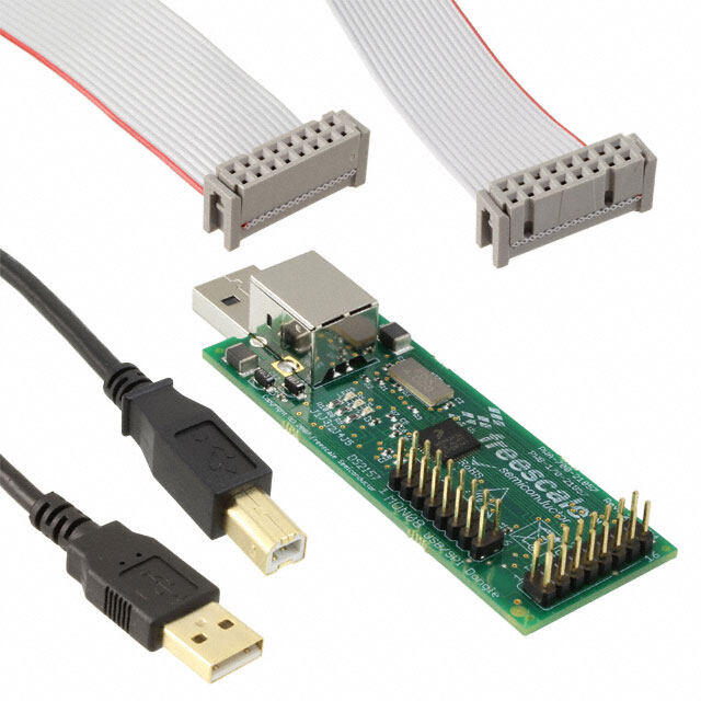
ICGOO电子元器件商城为您提供CDB5466U由Cirrus Logic设计生产,在icgoo商城现货销售,并且可以通过原厂、代理商等渠道进行代购。 CDB5466U价格参考¥2289.37-¥2289.37。Cirrus LogicCDB5466U封装/规格:评估和演示板和套件, CS5466 Energy/Power Meter Power Management Evaluation Board。您可以下载CDB5466U参考资料、Datasheet数据手册功能说明书,资料中有CDB5466U 详细功能的应用电路图电压和使用方法及教程。
| 参数 | 数值 |
| 产品目录 | 编程器,开发系统嵌入式解决方案 |
| 描述 | BOARD EVAL & SOFTWARE CS5466 ADC数据转换 IC 开发工具 Eval Bd F/Residental Pow-Meter Apps |
| 产品分类 | |
| 品牌 | Cirrus Logic |
| 产品手册 | |
| 产品图片 |
|
| rohs | 否含铅 / 不符合限制有害物质指令(RoHS)规范要求 |
| 产品系列 | 模拟与数字IC开发工具,数据转换 IC 开发工具,Cirrus Logic CDB5466U- |
| 数据手册 | |
| 产品型号 | CDB5466U |
| 主要属性 | 1 相,能量至频率输出 |
| 主要用途 | 电源管理,电度表/功率表 |
| 产品 | Evaluation Boards |
| 产品目录页面 | |
| 产品种类 | 数据转换 IC 开发工具 |
| 使用的IC/零件 | CS5466 |
| 其它名称 | 598-1011 |
| 商标 | Cirrus Logic |
| 商标名 | CDB546 |
| 封装 | Bulk |
| 嵌入式 | 是,MCU,8 位 |
| 工作电源电压 | 3.3 V to 5 V |
| 工具用于评估 | CS5466 |
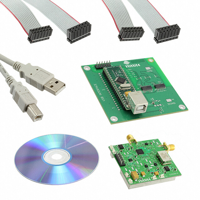
| 所含物品 | 板,线缆,软件 |
| 接口类型 | USB |
| 标准包装 | 1 |
| 相关产品 | /product-detail/zh/CS5466-ISZR/CS5466-ISZR-ND/2036787/product-detail/zh/CS5466-IS/598-1195-5-ND/1245645/product-detail/zh/CS5466-ISZ/598-1097-5-ND/923217 |
| 类型 | ADC |
| 系列 | CDB5466U |
| 辅助属性 | 图形用户界面,USB 接口 |


- 商务部:美国ITC正式对集成电路等产品启动337调查
- 曝三星4nm工艺存在良率问题 高通将骁龙8 Gen1或转产台积电
- 太阳诱电将投资9.5亿元在常州建新厂生产MLCC 预计2023年完工
- 英特尔发布欧洲新工厂建设计划 深化IDM 2.0 战略
- 台积电先进制程称霸业界 有大客户加持明年业绩稳了
- 达到5530亿美元!SIA预计今年全球半导体销售额将创下新高
- 英特尔拟将自动驾驶子公司Mobileye上市 估值或超500亿美元
- 三星加码芯片和SET,合并消费电子和移动部门,撤换高东真等 CEO
- 三星电子宣布重大人事变动 还合并消费电子和移动部门
- 海关总署:前11个月进口集成电路产品价值2.52万亿元 增长14.8%


PDF Datasheet 数据手册内容提取
\ CDB5466U CDB5466U Evaluation Board Features General Description (cid:122)Active Energy-to-Pulse Conversions The CS5466 is a low cost power/energy IC with pulse output for power measurement solutions. The (cid:122)Simple Configuration Jumpers CDB5466U Evaluation Board is an inexpensive tool – Current Channel Gain designed to evaluate the functionality and perfor- mance of the CS5466. – High-pass Filter – Energy-to-pulse Output Frequency The evaluation board is designed to output energy-to- pulse conversions upon power-up. The CS5466 data (cid:122) Energy Pulses sheet should be read and consulted when using the – Collected by On-board Microcontroller CDB5466U evaluation board. – Available on External Header The evaluation board includes a microcontroller with a – Viewable via LEDs USB interface. The microcontroller and GUI (Graphi- cal User Interface) provide a means to quickly register (cid:122)Multiple Supply Voltage Selections and evaluate the CS5466’s energy-to-pulse outputs. (cid:122)USB Communication with PC ORDERING INFORMATION (cid:122)On-board Voltage Reference CDB5466U Evaluation Board +5V GND VD+ EXT Vu+ EXT 4.096MHz XIN XOUT E1 E2 FOUT NEG E1 VIN+ VIN+ E2 C8051F320 CS5466 FOUT Microcontroller NEG VIN- VIN- USB HPF IIN+ IIN+ IGAIN0 IGAIN1 FREQ0 IIN- IIN- T U FREQ1 N O FI F FREQ2 E E R R V V CONFIGURATION JUMPERS VREF SOURCE REF+ +2.5 V Reference Copyright © Cirrus Logic, Inc. 2005 MAY ‘05 http://www.cirrus.com (All Rights Reserved) DS676DB1 1
CDB5466U TABLE OF CONTENTS LIST OF FIGURES ....................................................................................................................2 LIST OF TABLES ......................................................................................................................2 1. HARDWARE .............................................................................................................................3 1.1 Introduction ........................................................................................................................3 1.2 Evaluation Board Overview ................................................................................................3 1.2.1 Analog Section ......................................................................................................4 1.2.2 Digital Section .......................................................................................................5 1.2.3 Power Supply Section ...........................................................................................8 2. SOFTWARE ..............................................................................................................................9 2.1 Installation Procedure ........................................................................................................9 2.2 Using the Software .............................................................................................................9 2.2.1 Start-Up Window ...................................................................................................9 2.2.2 CS5466 Pulse Rate Output Window ...................................................................11 3. SCHEMATICS ........................................................................................................................13 4. LAYOUT .................................................................................................................................18 LIST OF FIGURES Figure 1. CDB5466U Assembly Drawing........................................................................................3 Figure 2. CDB5466U Start-up Window...........................................................................................9 Figure 3. Alert Window..................................................................................................................10 Figure 4. Quit Window...................................................................................................................10 Figure 5. CDB5466 Evaluation Board...........................................................................................11 Figure 6. CDB5466U Pulse Rate Output Window.........................................................................11 Figure 7. Analog Inputs.................................................................................................................13 Figure 8. CS546x and Socket.......................................................................................................14 Figure 9. CS5462 and CS5466 Configuration...............................................................................15 Figure 10. Microcontroller and USB Interface...............................................................................16 Figure 11. Power Supply...............................................................................................................17 Figure 1. Silk Screen.....................................................................................................................17 Figure 1. Topside Layer................................................................................................................18 Figure 1. Bottomside Layer...........................................................................................................19 LIST OF TABLES Table 1. Voltage Reference Selection for VREF.............................................................................4 Table 2. Voltage Reference Selection for VREF.............................................................................4 Table 3. Voltage and Current Channel Input Signal Selection........................................................5 Table 4. Current Channel PGA Selection........................................................................................6 Table 5. HPF Option Selection........................................................................................................6 Table 6. Energy Output Frequency.................................................................................................7 Table 7. Power Supply Connections...............................................................................................8 2 DS676DB1
CDB5466U 1. HARDWARE 1.1 Introduction The CS5466 is a low cost power measurement solution combining two ∆Σ analog-to-digital converters (ADCs), an energy-to-frequency converter, and energy pulse outputs on a single chip. It is designed to accurately measure and calculate energy for single phase, 2- or 3-wire power metering applications with minimal external components. Low-frequency energy outputs, E1 and E2 supply average active power and can be used to drive a stepper motor or a mechanical counter; the high-frequency energy output FOUT is designed to assist in calibration; and NEG in- dicates negative energy. The CS5466 has configuration pins which allow the selection of pulse output frequency, current channel input range, and the high-pass filter enable option. The CS5466 also has a power-on reset function which holds the part in reset until the supply reaches the proper level. The CDB5466U is shipped with a CS5466-ISZ device located at U6. 1.2 Evaluation Board Overview The CDB5466U evaluation board provides a quick path to evaluating the CS5466 Power Measurement IC. Figure 1 illustrates the placement of the terminals, jumpers and IC components. The jumper options are shown in the fac- tory default positions. +5V GND VD+_EXT Vu+_EXT JTAG USB J3 J4 J5 J6 J1 J2 JP1 TP1TP2 TP3 GND VD+ 8051_REGIN TP4 VD+_EXT Vu+_EXT GND VD+ +3+.53VV J8 V+5DV+ J9 TP5U3 8051 TP6 U4 JP2 GND JP3 RESS1ET 1LED_EN E1 GND J10 J11 J14 J12 1LED_EN E2 E1 EG RGENFD+ LTR10E1F+9 CDB5466U REV X TP7XOUTXINTP8Y1 JJ113511LLEEDD__EENN FNOEUGT RFENOSEUEEGTT2 EXT ENER R J23 4.096MHz J16 GND GND J17 U7 JP4 VIN+ VGRNEDF VIN+TP9 CPUCLK U5 GND VIN+ TP10 VIN- VIN- 6 GND VGRNEDF VINT-P11 546 J27 J22 GND J24 GND IIN+ J25 IIIINN+- VIRIIINNE+F- TP12 VA+GND VREFVREFINVREFOUT GNDVD+ GJNPJ5D28 J29 J30 J31 J32 J33 VREF TP13 VD+ GND JP6GND IIN- FOUT J26 GND GND FREQ2 FREQ1 FREQ0IGAIN1IGAIN0 HPF CS5466 CONFIG Figure 1. CDB5466U Assembly Drawing DS676DB1 3
CDB5466U The CDB5466U evaluation board is partitioned into two main sections - analog and digital. The analog section con- sists of the CS5466 and a precision voltage reference that operates from a single +5V power supply. The digital section consists of the microcontroller, the reset circuitry, and the USB interface. The digital section can operate from a +5V or +3.3V power supply. The evaluation board is epuipped with power supply connections that accommodate all of the various supply options of the CS5466. The evaluation board is designed to output energy-to-pulse conversions upon power-up. Software that runs on a PC provides a GUI (Graphical User Interface) as a means to quickly register and evaluate the CS5466’s energy-to-pulse outputs. To accomplish this, the board comes equipped with USB drivers and cable which physically interfaces the evaluation board to the PC. The software provides easy access to the energy outputs E1, E2, and FOUT and pro- vides a means to display and evaluate the performance of the CS5466. 1.2.1 Analog Section The CDB5466U evaluation board provides screw-type terminals (J23 and J27) to connect input signals to the volt- age and current channels. The screw terminals are labeled as VIN+, VIN-, IIN+, and IIN-. A simple R-C network at each channel input provides a simple anti-alias filter. The evaluation board provides three voltage reference options for VREFIN to the CS5466. The three voltage refer- ence options include: VREFOUT from the CS5466, the on-board +2.5V reference, and external REF+ (screw ter- minal J14). Table1 and Table2 illustrate the options available for VREFIN. With a jumper on J25 in the position Reference Description J25 Selects on-Chip VREFO VREFOUT Reference (25ppm/°C) VRE FINO VREFOUT(cid:134) ( D e f a u l t ) Selects External or VREFO VREF LT1019 Reference(J12) VRE FINO VREFOUT(cid:134) Table 1. Internal Voltage Reference Selection for VREF labeled VREFOUT, the reference is supplied by the on-chip voltage reference. With a jumper on J25 in the position labeled VREF, the reference is supplied by an off-chip voltage reference. Table2 illustrates the options available for VREF. With a jumper on J12 in position LT1019, the LT1019 provides a Reference Description J12 Selects on-Board LT1019 LT1019 Reference LT1019 (cid:134) O VREF RE F+ O O VREF (5ppm/°C) Selects External LT1019 (cid:134) O VREF REF+ Reference Source RE F+ O O VREF (J6) (Default) Table 2. External Voltage Reference Selection for VREF +2.5V reference (the LT1019 was chosen for its low drift - typically 5ppm/°C). By setting the jumper on J12 to posi- tion REF+, an external voltage reference is supplied via screw terminal J14’s REF+ input. The three input signal options for the voltage (VIN±) and current (IIN±) channel input include: an external signal (screw terminals J23 and J27), GND or VREF. Table3 illustrates the options available. By installing jumpers on J17 4 DS676DB1
CDB5466U to position VIN+, J22 to position VN-, J24 to position IIN+ and J26 to position IIN-, the input voltage signal is supplied from the screw terminals J23 and J27. With a jumper on J17, J22, J24 and J26 in the GND position, the inputs are connected to analog ground (AGND). With a jumper on J17, J22, J24 and J26 in position VREF, the inputs are con- nected to the reference voltage selected on J12. INPUT Description J17 J22 J24 J26 Selects External GND(cid:134) O VIN+ VIN-(cid:134) O VIN- GND(cid:134) O IIN+ IIN- (cid:134) O IIN- VIN± or IIN± V REFO O VIN+ V REFO O VIN- V REFO O IIN+ V REFO O IIN- Signal VIN+O O VIN+ GNDO O VIN- IIN+O O IIN+ GNDO O IIN- (Default) (Default) (Default) (Default) Selects External GND(cid:134) O VIN+ VIN-(cid:134) O VIN- GND(cid:134) O IIN+ IIN- (cid:134) O IIN- VIN± or IIN± Signal V REFO O VIN+ V REFO O VIN- V REFO O IIN+ VR EF O O IIN- VIN+O O VIN+ GNDO O VIN- IIN+O O IIN+ GNDO O IIN- Selects Grounding GND(cid:134) O VIN+ VIN-(cid:134) O VIN- GND(cid:134) O IIN+ IIN- (cid:134) O IIN- GND the Input V REFO O VIN+ V REFO O VIN- V REFO O IIN+ V REFO O IIN- VIN+O O VIN+ GNDO O VIN- IIN+O O IIN+ GNDO O IIN- Selects Reference GND(cid:134) O VIN+ VIN-(cid:134) O VIN- GND(cid:134) O IIN+ IIN- (cid:134) O IIN- VREFIN Source V REFO O VIN+ V REFO O VIN- V REFO O IIN+ V REFO O IIN- VIN+O O VIN+ GNDO O VIN- IIN+O O IIN+ GNDO O IIN- Table 3. Voltage and Current Channel Input Signal Selection 1.2.2 Digital Section The digital section contains the microcontroller, USB interface, JTAG header, reset circuitry, and an external inter- face header (J11). The microcontroller interfaces the energy pulses, E1, E2, and FOUT output by the CS5466 with the USB connection to the PC. The microcontroller also provides a hardware reset to the CS5466, which is level shifted to support both +3.3V and +5V digital operation. Interface header, J11, is provided to allow the CDB5466U to be connected to an external energy registration device. The energy output pins E1, E2, FOUT and NEG are routed to LEDs which provide a simple visual check of the energy output pulses. Jumpers J10, J13, J15 and J16 are equipped at the factory with jumpers to enable the LEDs. 1.2.2.1 Current Channel Gain To accommodate different current-sensing elements the current channel incorporates a programmable gain that can be set to one of four input ranges. Input pins IGAIN1 and IGAIN0 define the four gain selections and corresponding maximum input signal level. Jumpers J31 and J32 define the state of IGAIN1 and IGAIN0, respectively. Table4 il- lustrates the options available. With jumpers J31=J32=GND the gain is set to 10x. With jumpers J31=GND and J32=VD+ the gain is set to 50x. With jumpers J31=VD+ and J32=GND the gain is set to 100x. With jumpers J31=VD+ and J32=VD+ the gain is set to 150x. DS676DB1 5
CDB5466U Maximum Input Range IGAIN1 IGAIN0 J31 J32 VD+(cid:134) VD+(cid:134) ±250mV 10x IGA IN1O IGA IN0 O GNDO GNDO (Defau l t) (Default) VD+(cid:134) VD+(cid:134) ±50mV 50x IGA IN1 O IGAIN0 O GNDO GNDO VD+(cid:134) VD+(cid:134) ±25mV 100x IGA IN1 O IGA IN0 O GNDO GNDO VD+(cid:134) VD+(cid:134) ±16.67mV 150x IGA IN1 O IGA IN0 O GNDO GNDO Table 4. Current Channel PGA Selection 1.2.2.2 High-pass Filter By removing the offset from either channel, no error component will be generated at DC when computing the active (real) power. Input pin HPF defines the three options, and J33 defines the state of the HPF pin. – HPF is enabled in the voltage channel when jumper J33=GND. – HPF is enabled in the current channel when pin HPF is connected to pin FOUT. – High-Pass Filter (HPF) is disabled when jumper J33=VD+. HPF High Pass Filter Option J33 HPF Option Voltage HPFO O VD+ is in Voltage HPFO O FOUT Channel Channel HPFO (cid:134) GND (Default) HPF Option Current HPFO O VD+ Channel is in Current HPFO O FOUT Channel HPFO (cid:134) GND HPF Option HPFO O VD+ Disabled is Disabled HPFO O FOUT HPFO (cid:134) GND Table 5. HPF Option Selection 1.2.2.3 Energy Pulse Outputs The CS5466 provides three output pins for energy registration. The E1 and E2 pins provide a simple interface from which energy can be registered. These pins are designed to directly connect to a stepper motor or electromechanical counter. The E1 and E2 outputs are available on header J11, pins 1 and 3, respectively. The pulse rate on the E1 and E2 pins are in the range of 0 to 4 Hz and all frequency settings are optimized to be used with standard meter constants. The FOUT pin is designated for system calibration, the pulse rate can be selected to reach a frequency of 8000 Hz. The FOUT output is available on header J11, pin 5. 6 DS676DB1
CDB5466U 1.2.2.4 Selecting Frequency of E1 and E2 The pulse rate on E1 and E2 can be set to one of four frequency ranges. Input pins FREQ1 and FREQ0 determine the maximum frequency on E1 and E2 for sine wave inputs with zero phase shift. The frequency of E2 is equal to the frequency of E1 with active-low alternating pulses. Table6 illustrates the options available. The maximum frequency on the E1 and E2 output pins is determined by the position of the jumpers on J28, J29 and J30, if the maximum peak differential signal applied to both channels is a sine wave with zero phase shift. Maximum Frequency for a Sine Wave Frequency Select FREQ2 FREQ1 FREQ0 E1 or E2 E1+E2 FOUT J28 J29 J30 VD+O VD+O VD+O 0.125 Hz 0.25 Hz 64x(E1+E2) 16 Hz FRE Q2 O FRE Q1 O FRE Q0 O GND(cid:134) GND(cid:134) GND(cid:134) VD+O VD+O VD+O 0.25 Hz 0.5 Hz 32x(E1+E2) 16 Hz FRE Q2 O FRE Q1 O FRE Q0 O GND(cid:134) GND(cid:134) GND(cid:134) VD+O VD+O VD+O 0.5Hz 1.0 Hz 16x(E1+E2) 16 Hz FRE Q2 O FRE Q1 O FRE Q0 O GND(cid:134) GND(cid:134) GND(cid:134) VD+O VD+O VD+O 1.0 Hz 2.0 Hz 2048x(E1+E2) 4,096 Hz FRE Q2 O FRE Q1 O FRE Q0 O GND(cid:134) GND(cid:134) GND(cid:134) (Default) (Default) (Default) VD+O VD+O VD+O 0.125 Hz 0.25 Hz 128x(E1+E2) 32 Hz FRE Q2 O FRE Q1 O FRE Q0 O GND(cid:134) GND(cid:134) GND(cid:134) VD+O VD+O VD+O 0.25 Hz 0.5 Hz 64x(E1+E2) 32 Hz FRE Q2 O FRE Q1 O FRE Q0 O GND(cid:134) GND(cid:134) GND(cid:134) VD+O VD+O VD+O 0.5 Hz 1.0 Hz 32x(E1+E2) 32 Hz FRE Q2 O FRE Q1 O FRE Q0 O GND(cid:134) GND(cid:134) GND(cid:134) VD+O VD+O VD+O 1.0 Hz 2.0 Hz 16x(E1+E2) 32 Hz FRE Q2 O FRE Q1 O FRE Q0 O GND(cid:134) GND(cid:134) GND(cid:134) Table 6. Energy Output Frequency DS676DB1 7
CDB5466U 1.2.3 Power Supply Section Table7 illustrates the power supply connections to the evaluation board. The +5 binding post (J3) supplies the pos- itive analog supply (VA+) for the CS5466 and the +2.5V reference. The VD+_EXT binding post (J5) supplies the digital section of the CS5466 (VD+) and level shifters. Jumper J8 allows the VD+ supply to be sourced from the VD+_EXT binding post (J5), the +5V binding post (J3), or the regulated +3.3V supply derived from the microcon- troller. The Vu+_EXT (J6) binding post supplies the positive supply for the 8051 processor (8051_REGIN). Jumper J9 allows the 8051_REGIN supply to be sourced from either the Vu+_EXT binding post (J6), +5V binding post (J3) or VD+_EXT binding post (J5). Power Supplies Power Post Connections VD+ 8051-REGIN Analog (VA+) Digital (VD+) 8051 (Vu+) +5V GND VD+EXT VU+EXT J8 J9 VD+_EXT(cid:134) O VD+ Vu+_EXT(cid:134) O 8051 NC +5O O VD+ +5O O 8051 +3.3O O VD+ VD+ O O 8051 (Default) (Default) NC +5 V D + _ E X+T5(cid:134)O OO V VDD++ V u + _ E X+5T(cid:134)O O O 8 8005511 +3.3O O VD+ VD+ O O 8051 VD+_EXT(cid:134) O VD+ Vu+_EXT(cid:134) O 8051 NC +5O O VD+ +5O O 8051 +3.3O O VD+ VD+ O O 8051 +5 +5 +5 +5 0 VD+_EXT(cid:134) O VD+ Vu+_EXT(cid:134) O 8051 NC +5 O O VD+ +5O O 8051 +3.3O O VD+ VD+ O O 8051 +5 VD+_EXT(cid:134) O VD+ Vu+_EXT(cid:134) O 8051 +5O O VD+ +5O O 8051 +3.3O O VD+ VD+ O O 8051 +5 VD+_EXT(cid:134) O VD+ Vu+_EXT(cid:134) O 8051 NC +5O O VD+ +5O O 8051 +3.3O O VD+ VD+ O O 8051 VD+_EXT(cid:134) O VD+ Vu+_EXT(cid:134) O 8051 NC +5O O VD+ +5O O 8051 +3.3O O VD+ VD+ O O 8051 NC VD+_EXT(cid:134) O VD+ Vu+_EXT(cid:134) O 8051 +5 +5O O VD+ +5O O 8051 +3.3O O VD+ VD+ O O 8051 +5 +3.3 +5 +5 0 VD+_EXT(cid:134) O VD+ Vu+_EXT(cid:134) O 8051 NC +5O O VD+ +5O O 8051 +3.3O O VD+ VD+ O O 8051 +3.3 VD+_EXT(cid:134) O VD+ Vu+_EXT(cid:134) O 8051 +5 +5O O VD+ +5O O 8051 +3.3O O VD+ VD+ O O 8051 Table 7. Power Supply Connections 8 DS676DB1
CDB5466U 2. SOFTWARE The evaluation board comes with a USB cable to link the evaluation board to the PC. The evaluation software is available for download on the Cirrus Logic web site at http://www.cirrus.com/industrialsoftware and is designed to ® ® run under Windows 2000 or Windows XP. 2.1 Installation Procedure The CDB5466U is designed to perform active energy measurement and output energy pulse registration upon pow- ering up. Evaluation software is available to aid in registering energy pulse outputs. To install the software, go to the Cirrus Logic WEB site at http://www.cirrus.com/industrialsoftware and refer to application note AN278. 2.2 Using the Software Before launching the evaluation software, check all jumper settings on the CDB5466U evaluation board as de- scribed in Section 1, and connect the board to an open USB port on the PC using the provided cable. Once the board is powered on, the software program can be launched. 2.2.1 Start-Up Window When the software is launched, the Start-Up window will appear. This window contains information concerning the software’s title, revision number, copyright date, etc. See Figure 2. Figure 2. CDB5466U Start-up Window At the top of the screen is a menu bar which displays user options. The menu bar has three items; Menu, Setup and Quit. Initially Menu is disabled to prevent conflicts with other serial communications devices. After establishing com- munication with the CDB5466U evaluation board the Menu item will become available. DS676DB1 9
CDB5466U 2.2.1.1 Setup Setup presents the communication connections available to the CDB5466U Evaluation Board. The CDB5466U has one connection option available, USB. As depicted in Figure 2, if the USB setup is selected, the evaluation software will poll the CDB5466U, verifying the serial communication link is ready. At this point USB is checked indicating that the PC has successfully communicated with the CDB5466U Evaluation Board. If the evaluation software is unable to establish a communication link with the CDB5466U a message window will appear, indicating that the initial communication has failed. See Figure 3. Figure 3. Alert Window Check to verify that the USB cable is connected properly and the power supply is on and connected properly to the CDB5466U. 2.2.1.2 Quit Quit allows the user to exit the evaluation software. Upon selecting Quit, a message window appears and queries if exiting the evaluation software is desired. See Figure 4. Figure 4. Quit Window 10 DS676DB1
CDB5466U 2.2.1.3 Menu Menu allows one selection option, Pulse Rate Window. The Pulse Rate Window provides a means to register the energy-to-pulse outputs. See Figure 5. Figure 5. CDB5466 Evaluation Board Upon selecting Pulse Rate Window, the CS5466 Pulse Rate Output Window will appear. 2.2.2 CS5466 Pulse Rate Output Window The Pulse Rate Output Window provides a means to access the E1, E2 and FOUT pin of the CS5466. See Figure 6. Figure 6. CDB5466U Pulse Rate Output Window DS676DB1 11
CDB5466U In the CS5466 Pulse Rate Output Window, the Pulse Count, Frequency, Average Freq and Standard Deviation are displayed for the three energy-to-pulse outputs. Count Span: The Count Span entry allows for a time period to be specified for counting the energy pulses output by the CS5466. The Count Span is a decimal number having a range of 0.18<CountSpan<167,772, with units of seconds. Periods to Average: The Periods to Average entry allows an average to be performed on the pulses counted during the specified Count Span. The Periods to Average is an integer with a range of 1<PeriodstoAverage<10,000. Reset DUT: When this button is selected, the evaluation software will request the microcontroller to hardware reset the CS5466. The CS5466 will perform a reset as discussed in the CS5466 data sheet. Start/Stop: Initially the Stop button is hidden. When the Start button is selected, the evaluation software will instruct the microcontroller to start counting the energy-to-pulse outputs from the CS5466. At this time the Start button is disabled and the Stop button will appear. The evaluation software will then collect the Pulse Count over a duration of time specified (in seconds) by the Count Span. The counted pulses will then be averaged over the specified Pe- riods to Average entry. The Pulse Count and calculated Frequency, Average Freq and Standard Deviation will be displayed at the end of the cycle. 12 DS676DB1
CDB5466U 3. SCHEMATICS s ut p n g I o al n A 7. e r u g Fi DS676DB1 13
CDB5466U et k c o S d n a x 6 4 5 S C 8. e r u g Fi 14 DS676DB1
CDB5466U n o ti a r u g fi n o C 6 6 4 5 S C d n a 2 6 4 5 S C 9. e r u g Fi DS676DB1 15
CDB5466U e c a f r e t n B I S U d n a r e oll r nt o c o r c Mi 0. 1 e r u g Fi 16 DS676DB1
CDB5466U n ply ree p c u S S k er Sil ow 1. P e 1. ur 1 g e Fi r u g Fi DS676DB1 17
CDB5466U 4. LAYOUT r e y a L e d si p o T 1. e r u g Fi 18 DS676DB1
CDB5466U r e y a L e d si m o tt o B 1. e r u g Fi DS676DB1 19
CDB5466U 20 DS676DB1
CDB5466U Contacting Cirrus Logic Support For all product questions and inquiries contact a Cirrus Logic Sales Representative. To find one nearest you go to www.cirrus.com IMPORTANT NOTICE Cirrus Logic, Inc. and its subsidiaries ("Cirrus") believe that the information contained in this document is accurate and reliable. However, the information is subject to change without notice and is provided "AS IS" without warranty of any kind (express or implied). Customers are advised to obtain the latest version of relevant information to verify, before placing orders, that information being relied on is current and complete. All products are sold subject to the terms and conditions of sale supplied at the time of order acknowledgment, including those pertaining to warranty, indemnification, and limitation of liability. No responsibility is assumed by Cirrus for the use of this information, including use of this information as the basis for manufacture or sale of any items, or for infringement of patents or other rights of third parties. This document is the property of Cirrus and by furnishing this information, Cirrus grants no license, express or implied under any patents, mask work rights, copyrights, trademarks, trade secrets or other intellectual property rights. Cirrus owns the copyrights associated with the information contained herein and gives con- sent for copies to be made of the information only for use within your organization with respect to Cirrus integrated circuits or other products of Cirrus. This consent does not extend to other copying such as copying for general distribution, advertising or promotional purposes, or for creating any work for resale. CERTAIN APPLICATIONS USING SEMICONDUCTOR PRODUCTS MAY INVOLVE POTENTIAL RISKS OF DEATH, PERSONAL INJURY, OR SEVERE PROP- ERTY OR ENVIRONMENTAL DAMAGE ("CRITICAL APPLICATIONS"). CIRRUS PRODUCTS ARE NOT DESIGNED, AUTHORIZED OR WARRANTED FOR USE IN AIRCRAFT SYSTEMS, MILITARY APPLICATIONS, PRODUCTS SURGICALLY IMPLANTED INTO THE BODY, AUTOMOTIVE SAFETY OR SECURITY DE- VICES, LIFE SUPPORT PRODUCTS OR OTHER CRITICAL APPLICATIONS. INCLUSION OF CIRRUS PRODUCTS IN SUCH APPLICATIONS IS UNDERSTOOD TO BE FULLY AT THE CUSTOMER'S RISK AND CIRRUS DISCLAIMS AND MAKES NO WARRANTY, EXPRESS, STATUTORY OR IMPLIED, INCLUDING THE IMPLIED WARRANTIES OF MERCHANTABILITY AND FITNESS FOR PARTICULAR PURPOSE, WITH REGARD TO ANY CIRRUS PRODUCT THAT IS USED IN SUCH A MANNER. IF THE CUSTOMER OR CUSTOMER'S CUSTOMER USES OR PERMITS THE USE OF CIRRUS PRODUCTS IN CRITICAL APPLICA- TIONS, CUSTOMER AGREES, BY SUCH USE, TO FULLY INDEMNIFY CIRRUS, ITS OFFICERS, DIRECTORS, EMPLOYEES, DISTRIBUTORS AND OTHER AGENTS FROM ANY AND ALL LIABILITY, INCLUDING ATTORNEYS' FEES AND COSTS, THAT MAY RESULT FROM OR ARISE IN CONNECTION WITH THESE USES. Cirrus Logic, Cirrus, and the Cirrus Logic logo designs are trademarks of Cirrus Logic, Inc. All other brand and product names in this document may be trademarks or service marks of their respective owners. Windows is a registered trademark of Microsoft Corporation. DS676DB1 21