ICGOO在线商城 > 开发板,套件,编程器 > 评估板 - 数模转换器 (DAC) > CDB4350
- 型号: CDB4350
- 制造商: Cirrus Logic
- 库位|库存: xxxx|xxxx
- 要求:
| 数量阶梯 | 香港交货 | 国内含税 |
| +xxxx | $xxxx | ¥xxxx |
查看当月历史价格
查看今年历史价格
CDB4350产品简介:
ICGOO电子元器件商城为您提供CDB4350由Cirrus Logic设计生产,在icgoo商城现货销售,并且可以通过原厂、代理商等渠道进行代购。 CDB4350价格参考。Cirrus LogicCDB4350封装/规格:评估板 - 数模转换器 (DAC), CS4350 24 Bit 192k Samples Per Second Digital to Analog Converter (DAC) Evaluation Board。您可以下载CDB4350参考资料、Datasheet数据手册功能说明书,资料中有CDB4350 详细功能的应用电路图电压和使用方法及教程。
| 参数 | 数值 |
| 产品目录 | 编程器,开发系统 |
| DAC数 | 2 |
| DAC类型 | 电压 |
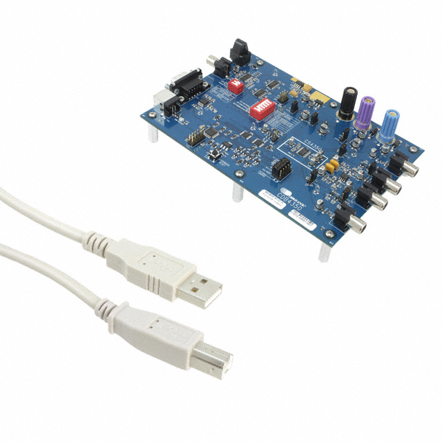
| 描述 | BOARD EVAL FOR CS4350 DAC |
| 产品分类 | 评估板 - 数模转换器 (DAC) |
| 品牌 | Cirrus Logic Inc |
| 数据手册 | |
| 产品图片 | |
| 产品型号 | CDB4350 |
| rohs | 含铅 / 不符合限制有害物质指令(RoHS)规范要求 |
| 产品系列 | - |
| 产品目录页面 | |
| 位数 | 24 |
| 使用的IC/零件 | CS4350 |
| 其它名称 | 598-1517 |
| 工作温度 | -40°C ~ 85°C |
| 建立时间 | - |
| 所含物品 | 板 |
| 数据接口 | 串行 |
| 标准包装 | 1 |
| 相关产品 | /product-detail/zh/CS4350-DZZR/CS4350-DZZR-ND/2036679/product-detail/zh/CS4350-CZZR/598-2334-2-ND/2036678/product-detail/zh/CS4350-CZZ/598-1185-5-ND/1245635/product-detail/zh/CS4350-DZZ/598-1184-5-ND/1245634 |
| 采样率(每秒) | 192k |



- 商务部:美国ITC正式对集成电路等产品启动337调查
- 曝三星4nm工艺存在良率问题 高通将骁龙8 Gen1或转产台积电
- 太阳诱电将投资9.5亿元在常州建新厂生产MLCC 预计2023年完工
- 英特尔发布欧洲新工厂建设计划 深化IDM 2.0 战略
- 台积电先进制程称霸业界 有大客户加持明年业绩稳了
- 达到5530亿美元!SIA预计今年全球半导体销售额将创下新高
- 英特尔拟将自动驾驶子公司Mobileye上市 估值或超500亿美元
- 三星加码芯片和SET,合并消费电子和移动部门,撤换高东真等 CEO
- 三星电子宣布重大人事变动 还合并消费电子和移动部门
- 海关总署:前11个月进口集成电路产品价值2.52万亿元 增长14.8%
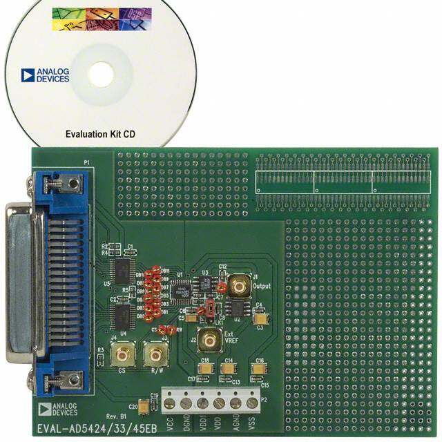


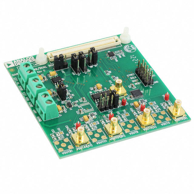
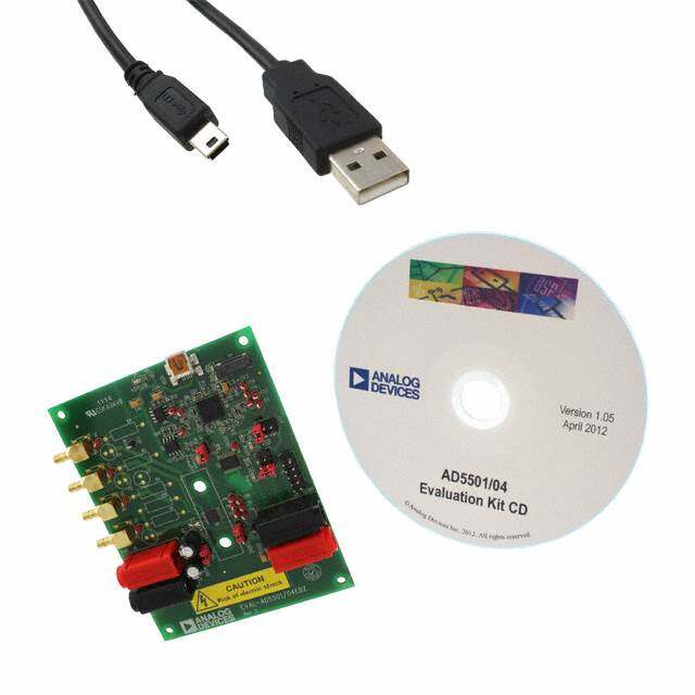
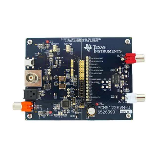
PDF Datasheet 数据手册内容提取
CDB4350 Evaluation Board for CS4350 Features Description The CDB4350 evaluation board is an excellent platform (cid:141) No High Frequency Master Clock Required for quickly evaluating the CS4350 24-bit, 24-pin, stereo D/A converter. Evaluation requires an analog signal an- (cid:141) Stand-Alone or PC GUI Board Control alyzer, a digital signal source, a PC for controlling the CS4350 (only required for Control Port Mode), and a (cid:141) CS8416 Receives S/PDIF-Compatible Digital power supply. Analog line-level outputs are provided via Audio RCA phono jacks. The CS8416 digital audio receiver IC provides the sys- (cid:141) Headers for External PCM Audio Input tem timing necessary to operate the digital-to-analog converter and will accept S/PDIF-compatible audio da- (cid:141) Demonstrates Recommended Layout and ta. The evaluation board may also be configured to Grounding Arrangements. accept external timing and data signals for operation in a user application during system development. (cid:141) Requires Only a Digital Signal Source and ORDERING INFORMATION Power Supplies for a Complete Digital-to- Analog Converter System CDB4350 Evaluation Board Hardware or Software Board Control Inputs for PCM Analog Outputs Clocks and Data and Filtering CS4350 CS8416 Recovered Master Digital Audio Clock Interface Copyright © Cirrus Logic, Inc. 2006 APRIL '06 http://www.cirrus.com (All Rights Reserved) DS691DB1
CDB4350 TABLE OF CONTENTS 1. CDB4350 SYSTEM OVERVIEW ............................................................................................................3 2. CS4350 DIGITAL-TO-ANALOG CONVERTER .....................................................................................3 3. CS8416 DIGITAL AUDIO RECEIVER ....................................................................................................3 4. INPUT FOR CLOCKS AND DATA .........................................................................................................3 5. INPUT FOR CONTROL DATA ...............................................................................................................3 6. POWER SUPPLY CIRCUITRY ...............................................................................................................4 7. GROUNDING AND POWER SUPPLY DECOUPLING ..........................................................................4 8. ANALOG OUTPUT FILTERING .............................................................................................................4 9. BOARD CONNECTIONS AND SETTINGS ............................................................................................5 10. SCHEMATICS ......................................................................................................................................6 11. LAYOUT .............................................................................................................................................13 12. REVISION HISTORY ..........................................................................................................................16 LIST OF FIGURES Figure 1.System Block Diagram and Signal Flow .......................................................................................6 Figure 2.CS4350 .........................................................................................................................................7 Figure 3.Analog Outputs .............................................................................................................................8 Figure 4.PCM Input Header and Hardware Control ....................................................................................9 Figure 5.CS8416 S/PDIF Input .................................................................................................................10 Figure 6.Control Port .................................................................................................................................11 Figure 7.Power ..........................................................................................................................................12 Figure 8.Silkscreen Top ............................................................................................................................13 Figure 9.Top Side ......................................................................................................................................14 Figure 10.Bottom Side ..............................................................................................................................15 LIST OF TABLES Table 1. System Connections .....................................................................................................................5 Table 2. CDB4350 Jumper Settings ............................................................................................................5 Table 3. CDB4350 Switch Settings .............................................................................................................5 2 DS691DB1
CDB4350 1. CDB4350 SYSTEM OVERVIEW The CDB4350 evaluation board is an excellent platform for quickly evaluating the CS4350. The CS8416 digital audio interface receiver provides an easy interface to digital audio signal sources including the majority of digital audio test equipment. The evaluation board also allows the user to supply external PCM clocks and data through headers for system development. The CDB4350 schematic has been partitioned into 6 pages, shown in Figures2 through 7. Each schematic page is represented in the system diagram shown in Figure1. Notice that the system diagram also includes the intercon- nections between the partitioned schematics. 2. CS4350 DIGITAL-TO-ANALOG CONVERTER A description of the CS4350 is included in the CS4350 datasheet, available at www.cirrus.com. 3. CS8416 DIGITAL AUDIO RECEIVER The system receives and decodes the standard S/PDIF data format using a CS8416 digital audio receiver (Figure5). The outputs of the CS8416 include a serial bit clock, serial data, and a left-right clock. The CS8416 data format is selected through switch S1. The operation of the CS8416 and a discussion of the digital audio interface is included in the CS8416 datasheet, available at www.cirrus.com. The CDB4350 has been designed so that the input can be either optical or coaxial (see Figure6). However, both inputs cannot be driven simultaneously. After the CS8416 serial format is changed either through S1 in Stand-Alone Mode, or though the CDB4350 GUI in PC Mode, a reset is required. The CS8416 can be manually reset using ‘HARDWARE RESET’ (S2) in Stand-Alone Mode, or through software when operating the CDB4350 in PC Mode. 4. INPUT FOR CLOCKS AND DATA The evaluation board has been designed to allow external PCM data input through header J10. The schematic for the clock/data input is shown in Figure4. In Stand-Alone Mode, switch position 6 of S4 selects the source as either CS8416 (open) or header J10 (closed). In PC Mode, the PCM source is selected through software. 5. INPUT FOR CONTROL DATA The evaluation board can be run in either a Stand-Alone Mode or with a PC. Stand-Alone Mode does not require the use of a PC, and the mode pins are configured using switch positions 1through5 of S4 and switch positions 1 and 2 of S1. PC Mode uses software to set up the CS4350 through I²C® or SPI™ using the PC’s serial port or USB port. When the serial port (RS232) or USB is attached and the CDB4350 software is running, PC Mode is automat- ically selected. Header J38 offers the option for external input of RST and SPI/I²C clocks and data. The board is set up from the factory to use the on-board microcontroller in conjunction with software available at www.cirrus.com. To use an ex- ternal control source, remove the shunts on J38 and place a ribbon cable so the signal lines are on the center row and the grounds are on the right side. R89 and R90 should be populated with 2kΩ resistors when using an external I²C source which does not already provide pull-ups. DS691DB1 3
CDB4350 6. POWER SUPPLY CIRCUITRY Power is supplied to the evaluation board by three binding posts (GND, +12V, and -12V), as shown in Figure7. The ‘+12V’ and ‘-12V’ terminals supply the active output filters. The +3.3V and +5.0V circuitry is powered by regulators fed by the ‘+12V’ terminal. Headers J3, J4, and J7 allow the user to either select +3.3V or +5.0V supplies for the various CS4350 voltage supply pins. Alternatively, the user can remove the shunts on J3, J4, and J7, and provide an external power supply. WARNING:Refer to the CS4350 datasheet for maximum allowable voltage levels. Operation outside of this range can cause permanent damage to the device. 7. GROUNDING AND POWER SUPPLY DECOUPLING As with any high-performance converter, the CS4350 requires careful attention to power supply and grounding ar- rangements in order to optimize performance. Figure2 details the connections to the CS4350 while Figures8, 9, and 10 show the component placement and top and bottom layout. The decoupling capacitors are located as close to the CS4350 as possible. Extensive use of ground plane fill in the evaluation board yields large reductions in ra- diated noise. 8. ANALOG OUTPUT FILTERING The analog output on the CDB4350 has been designed according to the CS4350 datasheet. This output circuit in- cludes an active 2-pole, 50kHz filter which utilizes the multiple-feedback topology and a passive output filter. 4 DS691DB1
CDB4350 9. BOARD CONNECTIONS AND SETTINGS Board connections and settings are shown in Table1, Table2, and Table3. CONNECTOR INPUT/OUTPUT SIGNAL PRESENT GND Input Ground connection from power supply +12V Input +12V positive supply for the on-board filtering -12V Input -12V negative supply for the on-board filtering S/PDIF IN - J1 Input Digital audio interface input via coax S/PDIF IN - OPT1 Input Digital audio interface input via optical PCM INPUT - J10 Input Input for master, serial, left/right clocks and serial data AOUTA, AOUTB Output RCA line level analog outputs from active output stage POUTA, POUTB Output RCA line level analog outputs from passive output stage Table 1. System Connections JUMPER PURPOSE POSITION FUNCTION SELECTED *A *CDB4350 outputs from AOUTA and AOUTB J6, J21 Selects analog output P CDB4350 outputs from POUTA and POUTB Selects Supply Voltage for +5V Supplies +5.0V to associated CS4350 supply J3, J4, J7 CS4350 *+3.3V *Supplies +3.3V to associated CS4350 supply *PC CONTROL *Control from PC and on-board microcontroller J38 Selects source of control data shunts removed External control input using center and right columns J27 C2 micro programming - Reserved for factory use only Table 2. CDB4350 Jumper Settings *Default Factory Settings. SWITCH (Note 1) PURPOSE POSITION FUNCTION SELECTED S2 Resets CS8416 and CS4350 The CS8416 must be reset if switch S1 is changed CS8416 Format Select Default: SFSEL[1:0] = 00 (Closed). See CS8416 datasheet S1 1,2 SFSEL[1:0] for details. CS4350 Format Select Default: DIF[2:0] = 000 (Closed). See CS4350 datasheet 1,2, 3 DIF[2:0] for details. open = De-emphasis enabled CS4350 De-emphasis Select 4 *closed = De-emphasis disabled. S4 open = Popguard enabled CS4350 Popguard Enable 5 *closed = Popguard disabled. Selects PCM source for *open = CS8416 6 CS4350 closed = PCM Header J10 Table 3. CDB4350 Switch Settings *Default Factory Settings. Note: 1. Switch settings take effect in Stand-Alone Mode only. DS691DB1 5
6 10.SCHEMATICS Power Serial Control Port Figure7 Figure6 P C M source select I2C/SPI Header Analog Outputs PCM HEADER POUTA Figure3 Figure4 PCM Clocks/Data 2 AOUTA Figure3 PCM mux CS4350 PCM Clocks/Data 2 AOUTB PCM Clocks/Data DIF[2:0] Figure3 Figure4 CS8416 Figure2 POUTB S/PDIF Figure3 Input CS8416 serial port PC format M Figure5 source select RMCK Header Figure4 Hardware Control Switches Figure4 C D D S Figure 1. System Block Diagram and Signal Flow B 6 9 4 1 3 D B 5 1 0
D S 6 9 1 D B 1 Figure 2. CS4350 C D B 4 3 5 7 0
8 C D D S B 6 9 Figure 3. Analog Outputs 4 1 3 D B 5 1 0
D S 6 9 1 D B 1 C D B 4 3 Figure 4. PCM Input Header and Hardware Control 5 9 0
1 0 C D D S B 69 Figure 5. CS8416 S/PDIF Input 4 1 3 D B 5 1 0
D S 6 9 1 D B 1 C D B Figure 6. Control Port 4 3 5 1 1 0
1 2 C D D S6 Figure 7. Power B 9 4 1 3 D B 5 1 0
D 11.LAYOUT S 6 9 1 D B 1 C D B 4 Figure 8. Silkscreen Top 3 5 1 3 0
1 4 C D D S B 6 9 4 1 3 DB Figure 9. Top Side 5 1 0
D S 6 9 1 D B 1 C D B 4 3 Figure 10. Bottom Side 5 1 5 0
CDB4350 12.REVISION HISTORY Release Date Changes DB1 April 2006 Initial Evaluation Board Datasheet Release Contacting Cirrus Logic Support For all product questions and inquiries, contact a Cirrus Logic Sales Representative. To find the one nearest to you, go to www.cirrus.com IMPORTANT NOTICE Cirrus Logic, Inc. and its subsidiaries ("Cirrus") believe that the information contained in this document is accurate and reliable. However, the information is subject to change without notice and is provided "AS IS" without warranty of any kind (express or implied). Customers are advised to obtain the latest version of relevant information to verify, before placing orders, that information being relied on is current and complete. All products are sold subject to the terms and conditions of sale supplied at the time of order acknowledgment, including those pertaining to warranty, indemnification, and limitation of liability. No responsibility is assumed by Cirrus for the use of this information, including use of this information as the basis for manufacture or sale of any items, or for infringement of patents or other rights of third parties. This document is the property of Cirrus and by furnishing this information, Cirrus grants no license, express or implied under any patents, mask work rights, copyrights, trademarks, trade secrets or other intellectual property rights. Cirrus owns the copyrights associated with the information contained herein and gives con- sent for copies to be made of the information only for use within your organization with respect to Cirrus integrated circuits or other products of Cirrus. This consent does not extend to other copying such as copying for general distribution, advertising or promotional purposes, or for creating any work for resale. CERTAIN APPLICATIONS USING SEMICONDUCTOR PRODUCTS MAY INVOLVE POTENTIAL RISKS OF DEATH, PERSONAL INJURY, OR SEVERE PROP- ERTY OR ENVIRONMENTAL DAMAGE (“CRITICAL APPLICATIONS”). CIRRUS PRODUCTS ARE NOT DESIGNED, AUTHORIZED OR WARRANTED FOR USE IN AIRCRAFT SYSTEMS, MILITARY APPLICATIONS, PRODUCTS SURGICALLY IMPLANTED INTO THE BODY, AUTOMOTIVE SAFETY OR SECURITY DE- VICES, LIFE SUPPORT PRODUCTS OR OTHER CRITICAL APPLICATIONS. INCLUSION OF CIRRUS PRODUCTS IN SUCH APPLICATIONS IS UNDERSTOOD TO BE FULLY AT THE CUSTOMER’S RISK AND CIRRUS DISCLAIMS AND MAKES NO WARRANTY, EXPRESS, STATUTORY OR IMPLIED, INCLUDING THE IMPLIED WARRANTIES OF MERCHANTABILITY AND FITNESS FOR PARTICULAR PURPOSE, WITH REGARD TO ANY CIRRUS PRODUCT THAT IS USED IN SUCH A MANNER. IF THE CUSTOMER OR CUSTOMER’S CUSTOMER USES OR PERMITS THE USE OF CIRRUS PRODUCTS IN CRITICAL APPLICA- TIONS, CUSTOMER AGREES, BY SUCH USE, TO FULLY INDEMNIFY CIRRUS, ITS OFFICERS, DIRECTORS, EMPLOYEES, DISTRIBUTORS AND OTHER AGENTS FROM ANY AND ALL LIABILITY, INCLUDING ATTORNEYS’ FEES AND COSTS, THAT MAY RESULT FROM OR ARISE IN CONNECTION WITH THESE USES. Cirrus Logic, Cirrus, the Cirrus Logic logo designs, and Popguard are trademarks of Cirrus Logic, Inc. All other brand and product names in this document may be trademarks or service marks of their respective owners. I²C is a registered trademark of Philips Semiconductor. SPI is a trademark of Motorola, Inc. 16 DS691DB1
 Datasheet下载