 Datasheet下载
- 型号: CD143A-SR05
- 制造商: Bourns
- 库位|库存: xxxx|xxxx
- 要求:
| 数量阶梯 | 香港交货 | 国内含税 |
| +xxxx | $xxxx | ¥xxxx |
查看当月历史价格
查看今年历史价格
CD143A-SR05产品简介:
ICGOO电子元器件商城为您提供CD143A-SR05由Bourns设计生产,在icgoo商城现货销售,并且可以通过原厂、代理商等渠道进行代购。 CD143A-SR05价格参考¥2.92-¥7.53。BournsCD143A-SR05封装/规格:TVS - 二极管, 20V Clamp 30A (8/20µs) Ipp Tvs Diode Surface Mount SOT-143。您可以下载CD143A-SR05参考资料、Datasheet数据手册功能说明书,资料中有CD143A-SR05 详细功能的应用电路图电压和使用方法及教程。
| 参数 | 数值 |
| 产品目录 | |
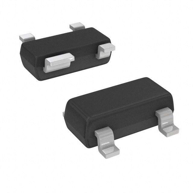
| 描述 | TVS DIODE 5VWM 20VC SOT143TVS二极管阵列 SOT 143 5V 500W Low Capacitance |
| 产品分类 | |
| 品牌 | Bourns |
| 产品手册 | |
| 产品图片 |
|
| rohs | 符合RoHS无铅 / 符合限制有害物质指令(RoHS)规范要求 |
| 产品系列 | 二极管与整流器,TVS二极管,TVS二极管阵列,Bourns CD143A-SR05- |
| 数据手册 | |
| 产品型号 | CD143A-SR05 |
| 不同频率时的电容 | 10pF @ 1MHz |
| 产品培训模块 | http://www.digikey.cn/PTM/IndividualPTM.page?site=cn&lang=zhs&ptm=4768 |
| 产品目录绘图 |
|
| 产品目录页面 | |
| 产品种类 | TVS二极管阵列 |
| 供应商器件封装 | SOT-143 |
| 其它名称 | CD143A-SR05DKR |
| 击穿电压 | 6 V |
| 功率-峰值脉冲 | 500W |
| 包装 | Digi-Reel® |
| 单向通道 | - |
| 双向通道 | 2 |
| 商标 | Bourns |
| 安装类型 | 表面贴装 |
| 安装风格 | SMD/SMT |
| 封装 | Reel |
| 封装/外壳 | TO-253-4,TO-253AA |
| 封装/箱体 | SOT-143 |
| 尺寸 | 1.39(Max) mm W x 3.04(Max) mm L |
| 峰值浪涌电流 | 30 A |
| 峰值脉冲功率耗散 | 500 W |
| 工作温度 | -55°C ~ 150°C |
| 工作电压 | 5 V |
| 工厂包装数量 | 3000 |
| 应用 | 以太网 |
| 最大工作温度 | + 155 C |
| 最小工作温度 | - 55 C |
| 极性 | Unidirectional |
| 标准包装 | 1 |
| 电压-击穿(最小值) | 6V |
| 电压-反向关态(典型值) | 5V(最小值) |
| 电压-箝位(最大值)@Ipp | 20V |
| 电容 | 10 pF |
| 电流-峰值脉冲(10/1000µs) | 30A (8/20µs) |
| 电源线路保护 | 是 |
| 端接类型 | SMD/SMT |
| 类型 | 转向装置(轨至轨) |
| 系列 | CD143A-SR05-12 |
| 通道 | 2 Channels |
| 钳位电压 | 9.8 V |


- 商务部:美国ITC正式对集成电路等产品启动337调查
- 曝三星4nm工艺存在良率问题 高通将骁龙8 Gen1或转产台积电
- 太阳诱电将投资9.5亿元在常州建新厂生产MLCC 预计2023年完工
- 英特尔发布欧洲新工厂建设计划 深化IDM 2.0 战略
- 台积电先进制程称霸业界 有大客户加持明年业绩稳了
- 达到5530亿美元!SIA预计今年全球半导体销售额将创下新高
- 英特尔拟将自动驾驶子公司Mobileye上市 估值或超500亿美元
- 三星加码芯片和SET,合并消费电子和移动部门,撤换高东真等 CEO
- 三星电子宣布重大人事变动 还合并消费电子和移动部门
- 海关总署:前11个月进口集成电路产品价值2.52万亿元 增长14.8%


PDF Datasheet 数据手册内容提取
NT Features Applications MPLIA ■ Lead free as standard ■ Ethernet - 10/100/1000 Base T O HS C ■ RoHS compliant* ■ Firewire and USB Ro * ■ Halogen free** ■ Portable electronics ■ ESD protection >25 kV ■ Video/graphic cards ■ Protects Vcc and two data lines CD143A-SR05~12 – Steering/TVS Diode Array Series General Information The CD143A-SR05 and CD143A-SR12 devices provides ESD, EFT and surge protection for the external ports of portable electronic devices such as cell phones, handheld electronics and personal computers. 4 REF GND 1 The ESD protection provided by the component enables a data port to withstand a minimum ±8 KV Contact / ±15 KV Air Discharge per the ESD test method specified in IEC 61000-4-2. The device measures 2.80 mm x 1.20 mm and is available in a SOT-143 package intended to be mounted directly onto an FR4 printed circuit board. The Bourns®device will meet IEC 61000-4-2 (ESD), IEC 61000-4-4 (EFT) and IEC 61000-4-5 (Surge) requirements. I/O 2 3 I/O Absolute Maximum Ratings, TA= 25 °C (Unless Otherwise Noted) Parameter Symbol Value Unit Peak Pulse Power (t = 8/20 µs)1 P 500 W p PP Peak Pulse Current (t = 8/20 µs) p -SR05 I 30 A PP -SR12 16 Operating Temperature T -55 ˚C to 150 ˚C ˚C J Storage Temperature T -55 ˚C to 150 ˚C ˚C STG Peak Forward Voltage (lf= 1 A 8/20 µs) VF 1.5 V Electrical Characteristics, TA= 25 °C (Unless Otherwise Noted) Parameter Symbol CD143A-SR05 CD143A-SR12 Unit Breakdown Voltage Minimum @ 1 mA 2 V 6.0 13.3 V BR Working Peak Voltage 2 V 5.0 12 V WM Clamping Voltage Maximum @ I = 1 A 2,3 V 9.8 19 V P C Clamping Voltage Maximum @ I 2,3 V 20 @ 28 A 30 @ 16 A V P C Leakage Current @ V 2 I 5.0 1.0 µA WM D Capacitance Maximum per Data Line @ 0 V, 1 MHz 4,5 C 10 10 pF J Notes: 1.See Peak Pulse Power vs. Pulse Time. 2. From Pin 4 to Pin 1. 3.See Pulse Wave Form. 4. From Pin 1 to Pin 3, Pin 1 to Pin 2, Pin 3 to Pin 4, Pin 2 to Pin 4. 5. GND is connected to ground, REF is connected to +V and input applies to V = V . V = 30 mV, F = 1 MHz. CC CC WM OSC * RoHS Directive 2002/95/EC Jan 27, 2003 including Annex. **Bourns follows the prevailing definition of “halogen free” in the industry. Bourns considers a product to be “halogen free” if (a) the Bromine (Br) content is 900 ppm or less; (b) the Chlorine (Cl) content is 900 ppm or less; and (c) the total Bromine (Br) and Chlorine (Cl) content is 1500 ppm or less. Specifications are subject to change without notice. Customers should verify actual device performance in their specific applications.
CD143A-SR05~12 – Steering/TVS Diode Array Series Product Dimensions This is a molded JEDEC SOT-143 device. It weighs approximately 35 mg and has a Dimensions flammability rating of UL 94V-0. The dimensions for the packaged device are shown below. 2.80 - 3.04 A (0.110 - 0.12) 1.78 - 2.03 A B (0.070 - 0.080) B 2.11 - 2.48 C (0.083 - 0.098) 1.20 - 1.39 D (0.047 - 0.055) D C G 0.39 - 0.50 E (0.015 - 0.020) 0.79 - 0.93 H F (0.031 - 0.037) 0.08 - 0.15 F E G (0.003 - 0.006) 0.46 - 0.60 H I DIMENSIONS: (INMCHMES) (0.018 - 0.024) 0.84 - 1.14 I (0.033 - 0.045) J K 0.72 - 0.83 J (0.028 - 0.033) 0.013 - 0.10 K (0.0005 - 0.004) Recommended Pad Layout Block Diagram This is the footprint recommended for this SOT-143 device. The device block diagram below includes the pin names and basic electrical connections associated with each channel. 2.85 (0.112) 1.90 4 REF (0.075) GND 1 0.85 (0.033) 1.90 1.05 2.75 I/O 2 3 I/O (0.075) (0.041) (0.108) 1.70 (0.067) Typical Part Marking 0.85 (0.033) CD143A-SR05................................................................................5A CD143A-SR12..............................................................................12A 1.20 0.80 0.85 (0.047) (0.031) (0.033) MM DIMENSIONS: (INCHES) Specifications are subject to change without notice. Customers should verify actual device performance in their specific applications.
CD143A-SR05~12 – Steering/TVS Diode Array Series Performance Graphs Peak Pulse Power vs Pulse Time Pulse Wave Form P – Peak Pulse Current (W) PP 101,,001000000 500 W, 8/20 µs Waveform – Peak Pulse Current (% of I) PP 11246802000000 tt td =e tt| TttItdPe =P=s/ t 28 2W 0µ asµv se form Parameters 10 I PP 0 0.01 1 10 100 1,000 10,000 0 5 10 15 20 25 30 td – Pulse Duration (µs) t – Time (µs) Typical Capacitance vs. Reverse Voltage Power Derating Curve 16 100 Peak Pulse Power 12 er 80 8/20 µs w pacitance - pF 8 % of Rated Po 4600 Ca 4 C - 20 Average Power 0 0 0 1 2 3 4 5 0 25 50 75 100 125 150 VR – Reverse Voltage - Volts TL – Lead Temperature (°C) How To Order CD 143A - SR 05 Common Code Chip Diode Package • 143A = SOT-143 Model SR = Steering Diode Array Working Peak Voltage 05 = 5.0 VWM(Volts) 12 = 12 VWM(Volts) Specifications are subject to change without notice. Customers should verify actual device performance in their specific applications.
CD143A-SR05~12 – Steering/TVS Diode Array Series Packaging Information The surface mount product is packaged in an 8 mm x 4 mm tape and reel format per EIA-481 standard. P 0 P1 d E T Index Hole 120 ° F D2 W A D1 D P B C Trailer Device Leader ....... ....... ....... ....... W1 End ....... ....... ....... ....... Start 10 pitches (min.) 10 pitches (min.) MM DIMENSIONS: (INCHES) Direction of Feed Item Symbol SOT-143 2.75 ±0.10 Carrier Width A (0.108 - 0.004) 3.30 ±0.10 Carrier Length B (0.130 - 0.004) 1.25 ±0.10 Carrier Depth C (0.049 - 0.004) 1.55 ±0.05 Sprocket Hole d (0.061 - 0.002) 178 Reel Outside Diameter D (7.008) 50.0 Reel Inner Diameter D1 (1.969) Min. 13.0 ±0.20 Feed Hole Diameter D2 (0.512 - 0.008) 1.75 ±0.10 Sprocket Hole Position E (0.069 - 0.004) 3.50 ±0.05 Punch Hole Position F (0.138 - 0.002) 4.00 ±0.10 Punch Hole Pitch P (0.157 - 0.004) 4.00 ±0.10 Sprocket Hole Pitch P0 (0.157 - 0.004) 2.00 ±0.05 Embossment Center P1 (0.079 - 0.002) 0.20 ±0.10 Overall Tape Thickness T (0.008 - 0.004) 8.00 ±0.20 Tape Width W (0.315 - 0.008) 14.4 Reel Width W1 (0.567) Max. Quantity per Reel — 3,000 Specifications are subject to change without notice. REV. 06/11 Customers should verify actual device performance in their specific applications.