ICGOO在线商城 > 射频/IF 和 RFID > RF 收发器 IC > CC8530RHAT
 Datasheet下载
- 型号: CC8530RHAT
- 制造商: Texas Instruments
- 库位|库存: xxxx|xxxx
- 要求:
| 数量阶梯 | 香港交货 | 国内含税 |
| +xxxx | $xxxx | ¥xxxx |
查看当月历史价格
查看今年历史价格
CC8530RHAT产品简介:
ICGOO电子元器件商城为您提供CC8530RHAT由Texas Instruments设计生产,在icgoo商城现货销售,并且可以通过原厂、代理商等渠道进行代购。 CC8530RHAT价格参考¥24.43-¥45.61。Texas InstrumentsCC8530RHAT封装/规格:RF 收发器 IC, IC 射频 TxRx + MCU 通用 ISM > 1GHZ 2.4GHz 40-VFQFN 裸露焊盘。您可以下载CC8530RHAT参考资料、Datasheet数据手册功能说明书,资料中有CC8530RHAT 详细功能的应用电路图电压和使用方法及教程。
Texas Instruments(德州仪器)的CC8530RHAT是一款RF(射频)收发器集成电路,广泛应用于低功耗、短距离无线通信领域。以下是其主要应用场景:

1. 智能家居与自动化:CC8530RHAT支持2.4GHz频段的无线通信,适用于智能家居设备如智能灯泡、温控器、门锁等。它能够实现设备之间的互联互通,帮助构建一个智能化的家庭环境。

2. 物联网(IoT)设备:在物联网应用中,CC8530RHAT可用于传感器节点、网关和其他边缘设备,提供稳定可靠的无线数据传输。它支持Zigbee、Thread等多种协议,确保不同设备之间的互操作性。

3. 工业控制与自动化:在工业环境中,CC8530RHAT可以用于无线传感器网络(WSN),监测温度、湿度、压力等参数,并将数据实时传输到中央控制系统。这有助于提高生产效率和安全性。

4. 医疗保健设备:该芯片也可应用于可穿戴健康监测设备,如心率监测器、血糖仪等。通过无线连接,这些设备可以将健康数据发送到手机或云端,方便用户和医生进行远程监控。

5. 消费电子:对于消费电子产品,如无线鼠标、键盘、游戏控制器等,CC8530RHAT提供了低延迟、高可靠性的无线连接方案,提升了用户体验。

6. 资产跟踪与管理:在物流和仓储管理中,CC8530RHAT可以集成到标签或传感器中,实现实时位置追踪和状态监测,优化库存管理和运输流程。

总之,CC8530RHAT凭借其低功耗、高性能的特点,在多个行业中都有广泛应用,特别是在需要短距离、低功耗无线通信的场景下表现尤为突出。
| 参数 | 数值 |
| 产品目录 | |
| 描述 | IC SOC W/RF 2.4GHZ LP 40VQFN射频收发器 PurePath Wireless 2.4GHz RF SoC |
| 产品分类 | RF 收发器集成电路 - IC |
| 品牌 | Texas Instruments |
| 产品手册 | |
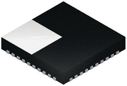
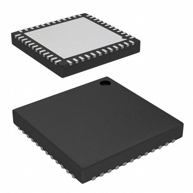
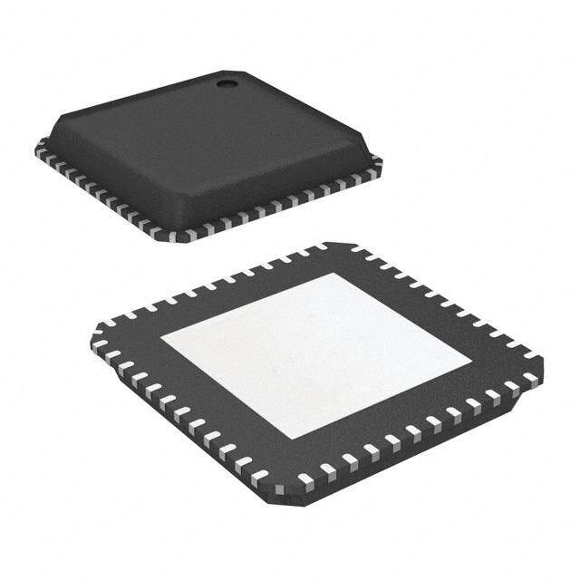
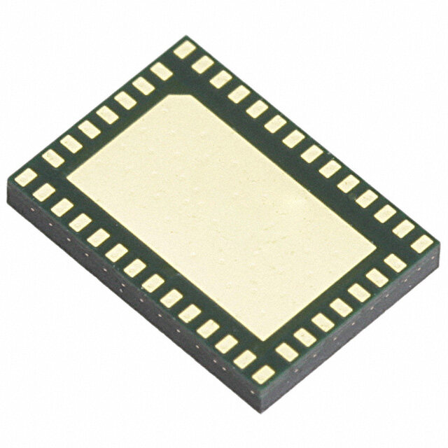
| 产品图片 |
|
| rohs | 符合RoHS无铅 / 符合限制有害物质指令(RoHS)规范要求 |
| 产品系列 | RF集成电路,射频收发器,Texas Instruments CC8530RHATPurePath™ 无线型 |
| 数据手册 | |
| 产品型号 | CC8530RHAT |
| PCN封装 | |
| PCN组件/产地 | |
| 产品种类 | 射频收发器 |
| 其它名称 | 296-29090-6 |
| 制造商产品页 | http://www.ti.com/general/docs/suppproductinfo.tsp?distId=10&orderablePartNumber=CC8530RHAT |
| 功率-输出 | 11dBm |
| 包装 | Digi-Reel® |
| 商标 | Texas Instruments |
| 天线连接器 | PCB,表面贴装 |
| 存储容量 | - |
| 安装风格 | SMD/SMT |
| 封装 | Reel |
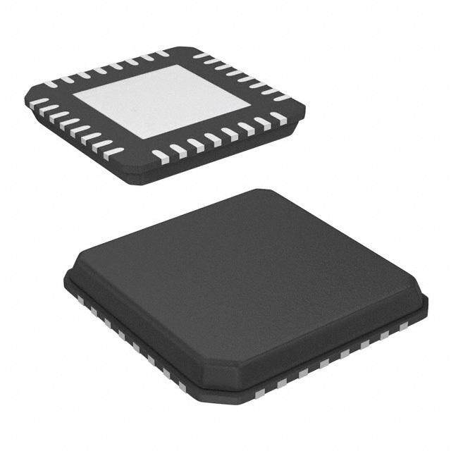
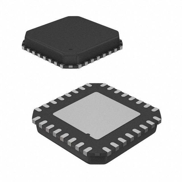
| 封装/外壳 | 40-VFQFN 裸露焊盘 |
| 封装/箱体 | VQFN-40 |
| 工作温度 | -40°C ~ 85°C |
| 工作电源电压 | 2 V to 3.6 V |
| 工厂包装数量 | 250 |
| 应用 | 音频系统 |
| 接口类型 | I2C, SPI |
| 数据接口 | PCB,表面贴装 |
| 数据速率(最大值) | 5Mbps |
| 最大工作温度 | + 85 C |
| 最大数据速率 | 5000 kb/s |
| 最小工作温度 | - 40 C |
| 标准包装 | 1 |
| 灵敏度 | -87dBm |
| 电压-电源 | 2 V ~ 3.6 V |
| 电流-传输 | - |
| 电流-接收 | - |
| 电源电压-最大 | 3.6 V |
| 电源电压-最小 | 2 V |
| 系列 | CC8530 |
| 调制或协议 | - |
| 输出功率 | 3.5 dBm |
| 频率 | 2.4GHz |
| 频率范围 | 2.4 GHz |


- 商务部:美国ITC正式对集成电路等产品启动337调查
- 曝三星4nm工艺存在良率问题 高通将骁龙8 Gen1或转产台积电
- 太阳诱电将投资9.5亿元在常州建新厂生产MLCC 预计2023年完工
- 英特尔发布欧洲新工厂建设计划 深化IDM 2.0 战略
- 台积电先进制程称霸业界 有大客户加持明年业绩稳了
- 达到5530亿美元!SIA预计今年全球半导体销售额将创下新高
- 英特尔拟将自动驾驶子公司Mobileye上市 估值或超500亿美元
- 三星加码芯片和SET,合并消费电子和移动部门,撤换高东真等 CEO
- 三星电子宣布重大人事变动 还合并消费电子和移动部门
- 海关总署:前11个月进口集成电路产品价值2.52万亿元 增长14.8%


PDF Datasheet 数据手册内容提取
CC8520, CC8521, CC8530(cid:15) CC8531 www.ti.com SWRS091F – JUNE 2012 2.4 GHz RF SoC FOR WIRELESS DIGITAL AUDIO STREAMING CC8520, CC8521, CC8530 & CC8531 - PurePath™ Wireless APPLICATIONS - Suited for systems targeting compliance - Wireless high-quality digital audio with worldwide radio frequency - Wireless point-to-point audio link regulations: ETSI EN 300 328 and EN - Wireless (USB) headphones / headsets 300 440 class 2 (Europe), FCC CFR47 Part - Wireless (USB) loudspeakers 15 (US) and ARIB STD-T66 (Japan) - Wireless (USB) microphones Digital audio support - Wireless 2.1 speaker systems - Digital I2S audio interface supports 1 or 2 - CC852x supports up to 2 channels audio channels for the CC8520 and 1 to 4 - CC853x supports up to 4 channels audio channels for the CC8530 at sample - CC85x1 supports USB rates of 32, 40.275, 44.1 and 48 kHz, and supports 16 and 24 bit word-widths FEATURES - USB audio support for 32, 44.1 and 48 kHz, Built-in audio protocol and supports 16 and 24 bit word-widths - CD-quality uncompressed audio - Audio latency down to 10.7 ms - Excellent robustness and co-existence - Data side-channel allows data to be sent through multiple techniques alongside the audio between external host - Adaptive Frequency Hopping processors - Forward Error Correction USB - Buffering and Retransmission - Full-speed USB Audio device - Error Concealment - USB Basic Audio Device Class: HT1, HS1 - Optional high quality audio and MT topologies (headphone, headset compression and microphone) - No software development needed when - USB Audio Device Class. used in autonomous mode - Basic USB HID device class support for External system remote control, mouse and keyboard - Can be used autonomously, or can be functionality controlled by an external host MCU for - Autonomous operation only. greatest flexibility Development tools - Seamless connection and control of - PC-based PurePath™ Wireless external audio codecs, DACs/ADCs and Configurator for CC85xx configuration digital audio amplifiers using I2S and I2C - CC85xx Family User Guide - HID functions like power control, pairing, - CC85XXDK audio development kit volume control, audio channel selection - CC85XXDK-HEADSET development kit etc. can be mapped to I/Os - RoHS compliant 6mm x 6mm QFN-40 package QFN-40 PIN CONFIGURATION (TOP VIEW) RF section 40 39 38 37 36 35 34 33 32 31 -- 5B aonr d2w Midbtphs-e offviceire-tnhte m-aoird dualattai ornat feo rmat 1 x/UASNBTPNDVDD DCPL xLNAEN/GIO15 IOVDD xPAEN/GIO14GIOI3 GIOI2 SDA/GIO11SCL/GIO10 AVDDRBIAS 30 2 xANTP VBAT 29 - Excellent link budget with programmable /USBN 3 CSN AVDD 28 output power up to +3.5 dBm and -83/-86 4 SCLK AVDD 27 dBm sensitivity 5 MOSI CC85xx AVDD 26 - Seamless support for CC2590 range 6 MISO RF_N 25 extender (+11dBm output power, -87dBm 7 GIO1 RF_P 24 sensitivity) 8 GIO2 AVDD 23 9 GIO3 X0 22 10 IOVDD X1 21 RSTN IOVDDMCLK/GIO4BCLK/GIO5WCLK/GIO6AD0/GIO7AD1/GIO8 IOVDD AD2/GIO9AVDD 1 2 3 4 5 6 7 8 9 0 1 1 1 1 1 1 1 1 1 2 PRODUCTION DATA information is current as of publication date. Products conform to specifications per the terms of Texas Instruments standard warranty. Production processing does not necessarily include testing of all parameters. Please be aware that an important notice concerning availability, standard warranty, and use in critical applications of Texas Instruments semiconductor products and disclaimers thereto appears at the end of this data sheet. PurePath™ is a trademark for Texas Instruments All other trademarks are the property of their respective owners. Copyright © 2010, Texas Instruments Incorporated
CC8520, CC8521, CC8530(cid:15) CC8531 WWW.TI.COM SWRS091F – JUNE 2012 DESCRIPTION The PurePath™ Wireless platform is a cost-effective and low-power solution optimized for wireless transmission of high-quality digital audio. The CC85xx includes a robust built-in wireless audio transmission protocol and can control selected external audio devices. Utilizing numerous coexistence mechanisms allows the CC85xx to avoid interfering with, or being interfered by other 2.4 GHz radio systems. The CC85xx operates autonomously, and can be used with or without an external MCU. An external host processor can be connected through SPI and control some aspects of its operation. The CC85xx interfaces easily with other TI audio ICs and DSPs (using I2S and DSP/TDM interfaces). More details can be found in the CC85xx Family User Guide [2]. ABBREVIATIONS ADC Analog to Digital Converter LED Light Emitting Diode ARIB Association of Radio Industries and Businesses LNA Low Noise Amplifier BER Bit Error Rate MISO Master In Slave Out CODEC Coder/Decoder MOSI Master Out Slave In DAC Digital to Analog Converter MCU Microcontroller DSP Digital Signal Processor PA Power Amplifier EHIF External Host Interface PCM Pulse Code Modulation ESD Electro Static Discharge PER Packet Error Rate ETSI European Telecommunications Standard Institute PLL Phase Lock Loop FCC Federal Communications Commission PM Protocol Master FEC Forward Error Correction PPW PurePath™ Wireless FSK Frequency Shift Keying PS Protocol Slave FW Firmware RoHS Restriction of Hazardous Substances HID Human Interface Device RF Radio Frequency I2C Inter-Integrated Circuit (serial communications bus) SLAC Slightly Lossy Compression Algorithm I2S Inter-IC Sound (serial bus for digital audio signals) SPI Serial Peripheral Interface IEEE Institute of Electrical and Electronics Engineers SoC System-on-Chip ISM Industrial, Scientific, Medical STD Standard JEDEC Joint Electron Device Engineering Council TDM Time-Division Multiplexing LDO Low-Dropout Regulator 2 Copyright © 2010, Texas Instruments Incorporated
CC8520, CC8521, CC8530(cid:15)C8531 WWW.TI.COM SWRS091F – JUNE 2012 This integrated circuit can be damaged by ESD. Texas Instruments recommends that all integrated circuits be handled with appropriate precautions. Failure to observe proper handling and installation procedures can cause damage. ESD damage can range from subtle performance degradation to complete device failure. Precision integrated circuits may be more susceptible to damage because very small parametric changes could cause the device not to meet its published specifications. ABSOLUTE MAXIMUM RATINGS(1) PARAMETER TEST CONDITIONS Min Max Unit Supply voltage (2) All supply pins must have the same voltage –0.3 3.9 V Voltage on any digital pin –0.3 min(VDD + V 0.3, 3.9) Input RF level 10 dBm Storage temperature range -40 125 °C ESD (3) All pads, according to human-body model 2000 V (HBM), JEDEC STD 22, method A114 According to charged-device model (CDM), 400 V JEDEC STD 22, method C101E (1) Stresses beyond those listed under Absolute Maximum Ratings may cause permanent damage to the device. These are stress ratings only, and functional operation of the device at these or any other conditions beyond those indicated under Recommended Operating Conditions is not implied. Exposure to absolute-maximum-rated conditions for extended periods may affect device reliability. (2) For CC8521 and CC8531 running on USB power, a LDO is needed to comply with these ratings. (3) CAUTION: ESD sensitive device. Precaution should be used when handing the device in order to prevent permanent damage. RECOMMENDED OPERATING CONDITIONS, CC8520/CC8530 PARAMETER TEST CONDITIONS Min Max Unit Operating ambient temperature range, T -40 +85 °C A Operating supply voltage 2.0 3.6 V RECOMMENDED OPERATING CONDITIONS, CC8521/CC8531 PARAMETER TEST CONDITIONS Min Max Unit Operating ambient temperature range, T -40 +85 °C A Operating supply voltage (1) 3.0 3.6 V (1) For CC8521 and CC8531 running on USB power, an LDO is needed to comply with these ratings. 3 Copyright © 2010, Texas Instruments Incorporated
CC8520, CC8521, CC8530(cid:15) CC8531 WWW.TI.COM SWRS091F – JUNE 2012 GENERAL CHARACTERISTICS Measured on Texas Instruments CC85xxEM reference designs with T = 25°C and VDD = 3.3 V, unless otherwise noted. A PARAMETER TEST CONDITION MIN TYP MAX UNIT RF frequency range 2400 2483.5 MHz Shaped 8FSK 5 Data rate Mbps Shaped 2FSK 2 Latency between I2S interface on audio source Audio latency and I2S interface on audio sink. Uncompressed 512(1) 2048 Samples 16 or 24 bit. Audio latency is programmable using the PurePath Wireless Configurator [1]. 48 Audio sample rate is programmable using the 44.1 Audio sample rate PurePath Wireless Configurator [1] (2) 40.275(3) kHz 32 (1) Latencies below 768 samples only supported for some configurations (2) ±2000ppm tolerance (3) Not supported in USB mode. For USB Headset, dynamic sample rate change is not allowed. ELECTRICAL CHARACTERISTICS, CC8520/CC8521/CC8530/CC8531 Measured on Texas Instruments CC85xxEM reference designs with T = 25°C and VDD = 3.3 V, unless otherwise noted. A PARAMETER TEST CONDITION MIN TYP MAX UNIT Current consumption, Voltage regulator / crystal oscillator off – status 1 A power down state lost (POWERED_DOWN state) Current consumption, headphone Average current for a PurePath Wireless master 29 mA master(1) with I2S interface active, sourcing two PCM16 channels with maximum output power. Current consumption, headphone Average current for a PurePath Wireless slave 25 mA slave(1) with I2S interface active, sinking two PCM16 channels with maximum output power (1) Measured on Texas Instruments CC85xx EM reference designs and CC85XXDK. Sample rate 48 kHz, MCLK disabled. 5 Mbit mode RF CHARACTERISTICS, CC8520/CC8521/CC8530/CC8531 Measured on Texas Instruments CC85xx EM reference designs with T = 25°C and VDD = 3.3 V, unless otherwise noted. A PARAMETER TEST CONDITION MIN TYP MAX UNIT Output power Maximum output power setting 3.5 dBm Receiver sensitivity(1) 52 MMbbppss (2) --8836 dBm 5 Mbps -2 Saturation (maximum input level) (1) 2 Mbps(2) 6 dBm Adjacent channel, ±4MHz, wanted 3dB above sensitivity. 5 Mbps 8 dB Adjacent channel, ±4MHz, wanted 3dB above 20 sensitivity. 2 Mbps(2) Selectivity Alternate channel, ±8MHz, wanted 3dB above sensitivity. 5 Mbps 35 dB Alternate channel, ±8MHz, wanted 3dB above 43 sensitivity. 2 Mbps(2) Occupied bandwidth 99% energy bandwidth. 5 Mbps 3.8 MHz 99% energy bandwidth. 2 Mbps(2) 3.2 Optimum load impedance Differential impedance seen from the RF port 70 + j30 Ω (RF_P and RF_N) towards the antenna Spurious emission Suitable for systems targeting compliance with EN 300 328, EN 300 440(3), FCC CFR47 Part 15 and ARIB STD-T-66 (1) Measured using data packets with 40 byte payload, 0.1% BER for 5 Mbit and 125 byte payload, 0.001% BED for 2 Mbit (2) Typical data measured across 6 devices at room temperature. (3) Systems with external antenna connector: Margins for passing conducted requirements at sub 1GHz frequencies can be improved by using a simple band-pass filter connected between matching network and RF connector (1.6 pF in parallel with 1.6 nH); this filter must be connected to a good RF ground. 4 Copyright © 2010, Texas Instruments Incorporated
CC8520, CC8521, CC8530(cid:15) CC8531 WWW.TI.COM SWRS091F – JUNE 2012 ELECTRICAL CHARACTERISTICS, CC8520/CC8521/CC8530/CC8531+CC2590 Measured on Texas Instruments CC85xx+CC2590 EM reference designs with T = 25°C and VDD = 3.3 V, unless otherwise noted. A PARAMETER TEST CONDITION MIN TYP MAX UNIT Current consumption, Voltage regulator / crystal oscillator off – status power down state(1) lost (POWERED_DOWN state) 1 A Average current for a PurePath Wireless Current consumption, headphone master(2) master with I2S interface active, sourcing two 38 mA PCM16 channels. Average current for a PurePath Wireless slave Current consumption, headphone slave(2) with I2S interface active, sinking two PCM16 28 mA channels (1) CC2590 power down current is 100 nA[4] (2) Measured on Texas Instruments CC85xx+CC2590 EM reference designs and CC85XXDK. Sample rate 48 kHz, MCLK disabled. 5 Mbit mode RF CHARACTERISTICS, CC8520/CC8521/CC8530/CC8531+CC2590 Measured on Texas Instruments CC85xx+CC2590 EM reference designs with T = 25°C and VDD = 3.3 V, unless otherwise noted. A PARAMETER TEST CONDITION MIN TYP MAX UNIT Output power Maximum output power setting 11 dBm Receiver sensitivity(1) 52 MMbbppss (2 ) --8970 dBm Saturation (maximum input level)(1) 5 Mbps -12 dBm Adjacent channel, ±4MHz, wanted 3dB above 9 sensitivity. 5 Mbps Selectivity dB Alternate channel, ±8MHz, wanted 3dB above 34 sensitivity. 5 Mbps Suitable for systems targeting compliance with EN 300 328, EN 300 440(3), FCC CFR47 Part 15 Spurious emission and ARIB STD-T-66 (1) Measured using data packets with 40 byte payload, 0.1% BER for 5 Mbit and 125 byte payload, 0.001% BER for 2 Mbit (2) Typical data measured across 6 devices at room temperature. (3) Systems with external antenna connector: Margins for passing conducted requirements at sub 1GHz frequencies can be improved by using a simple band-pass filter connected between matching network and RF connector (1.6 pF in parallel with 1.6 nH); this filter must be connected to a good RF ground. 48-MHz CRYSTAL REQUIREMENTS General parameters with T = 25°C and VDD = 3.3 V, unless otherwise noted. A PARAMETER TEST CONDITION MIN TYP MAX UNIT Crystal frequency 48 MHz Crystal frequency accuracy requirement(1) -50 50 ppm ESR Equivalent series resistance - 60 ohm C Crystal shunt capacitance - 3 pF 0 C Crystal load capacitance 15 16 17 pF L (1) Including aging and temperature dependency AUDIO CLOCK CHARACTERISTICS T = 25°C and VDD = 3.3 V, unless otherwise noted. A PARAMETER TEST CONDITION MIN TYP MAX UNIT Programmable using the PurePath Wireless MCLK Frequency range Configurator [1] 32·FWCLK 512·FWCLK Programmable using the PurePath Wireless BCLK Frequency range Configurator [1] 32·FWCLK 256·FWCLK WCLK Frequency range 31.936 48.096 kHz RMS jitter (Output clocks) RMS period jitter for 1000 periods 80 200 ps 5 Copyright © 2010, Texas Instruments Incorporated
CC8520, CC8521, CC8530(cid:15) CC8531 WWW.TI.COM SWRS091F – JUNE 2012 SPI INTERFACE CHARACTERISTICS T = 25°C and VDD = 3.3 V, unless otherwise noted. A PARAMETER TEST CONDITION MIN TYP MAX UNIT SCLK frequency 0 20 MHz SCLK low 25 ns SCLK high 25 ns CSN high Minimum time CSN must be high, if brought 50 ns high, between commands (it is not necessary to bring CSN high between commands). CSN falling edge to Distance from CSN asserted until first rising 25 ns SCLK rising edge edge on SCLK. SCLK falling edge to Distance from last negative edge of SCLK in 100 ns CSN rising edge last word until CSN can be de-asserted. Inter-word spacing Minimum distance in time from rising edge of 50 ns SCLK for last bit in word n and the rising edge of SCLK for the first bit in word n+1. Properly handles abutting words. Hysteresis on SCLK Hysteresis around trigger point of input buffer 100 mV using a Schmitt trigger Slew rate on SCLK Slew rate from 0.1·IOVDD to 0.9·IOVDD 10 V/ s VBAT CHARACTERISTICS T = 25°C and VDD = 3.3 V, unless otherwise noted. A PARAMETER TEST CONDITIONS Min Max Unit Input voltage 0 4.5 V FLASH CHARACTERISTICS T = 25°C and VDD = 3.3 V, unless otherwise noted. A PARAMETER TEST CONDITIONS Min TYP Max Unit Program/erase endurance 1000 Cycles 6 Copyright © 2010, Texas Instruments Incorporated
CC8520, CC8521, CC8530(cid:15) CC8531 WWW.TI.COM SWRS091F – JUNE 2012 1 PIN DESCRIPTION 0 9 8 7 6 5 4 3 2 1 4 3 3 3 3 3 3 3 3 3 1 x/UASNBTNNDVDD DCPL xLNAEN/GIO15 IOVDD xPAEN/GIO14 GIOI3 GIOI2 SDA/GIO11SCL/GIO10 AVDDRBIAS 30 2 xANTP VBAT 29 /USBP 3 CSN AVDD 28 4 SCLK AVDD 27 CC85xx 5 MOSI AVDD 26 6 MISO RF_N 25 7 GIO1 RF_P 24 8 GIO2 AVDD 23 9 GIO3 X0 22 10 IOVDD X1 21 RSTN IOVDD MCLK/GIO4BCLK/GIO5WCLK/GIO6AD0/GIO7AD1/GIO8 IOVDD AD2/GIO9 AVDD 1 2 3 4 5 6 7 8 9 0 1 1 1 1 1 1 1 1 1 2 Figure 1 - CC85xx QFN-40 PIN CONFIGURATION PIN PIN NAME PIN TYPE DESCRIPTION - GND Ground The exposed die attach pad must be connected to a solid ground plane underneath the chip 1 xANTN Digital I/O1 CC85x0 Slaves: External antenna switch control USBN CC85x1: USB D- data line 2 xANTP Digital I/O1 CC85x0 Slaves: External antenna switch control USBP CC85x1: USB D+ data line 3 CS_N Digital Input Serial SPI configuration interface, active low chip select (pull-up) 4 SCLK Digital I/O1 Serial SPI configuration interface, clock input/output 5 MOSI Digital I/O1 Serial SPI configuration interface, master data output, slave data input 6 MISO Digital I/O1 Serial SPI configuration interface, master data input, slave data output. 7 GIO1 Digital I/O1 General-purpose digital I/O pin 1 Configurable with PurePath™ Wireless Configurator 8 GIO2 Digital I/O1 General-purpose digital I/O pin 2 9 GIO3 Digital I/O2 General-purpose digital I/O pin 3 Configurable with PurePath™ Wireless Configurator 10 IOVDD Power Digital power supply for the digital I/Os in the SPI interface and GIO1-GIO3. (I/O pads) 11 RSTN Digital Input Active-low device reset (pull-up) 12 IOVDD Power Digital power supply for the RSTN and MCLK digital I/O pins. (I/O pins) 13 MCLK Digital I/O1 Master clock output for external audio devices GIO4 General-purpose digital I/O pin 4 7 Copyright © 2010, Texas Instruments Incorporated
CC8520, CC8521, CC8530(cid:15) CC8531 WWW.TI.COM SWRS091F – JUNE 2012 PIN PIN NAME PIN TYPE DESCRIPTION 14 BCLK Digital I/O1 I2S/DSP audio interface bit clock (in/out) GIO5 General-purpose digital I/O pin 5 15 WCLK Digital I/O1 I2S/DSP audio interface word clock (in/out) GIO6 General-purpose digital I/O pin 6 16 AD0 Digital I/O1 I2S/DSP audio interface data line 0 (in/out) GIO7 General-purpose digital I/O pin 7 17 AD1 Digital I/O1 I2S/DSP audio interface data line 1 (in/out) GIO8 General-purpose digital I/O pin 8 18 IOVDD Power Digital power supply for the digital I/Os in audio interface (BCLK-AD2). (I/O pins) 19 AD2 Digital I/O2 I2S/DSP audio interface data line 2 (in/out) GIO9 Configurable with PurePath™ Wireless Configurator 20 AVDD Power (Analog) 2.0-3.6V analog power supply connection 21 X1 Analog I/O Crystal oscillator pin input, or external clock input (48 MHz) 22 X0 Analog I/O Crystal oscillator pin output (48 MHz) 23 AVDD Power (Analog) Analog power supply connection 24 RF_P RF I/O Positive differential RF input signal to LNA in receive mode Positive differential RF output signal from PA in transmit mode 25 RF_N RF I/O Negative differential RF input signal to LNA in receive mode Negative differential RF output signal from PA in transmit mode 26 AVDD Power (Analog) Analog power supply connection 27 AVDD Power (Analog) Analog power supply connection 28 AVDD Power (Analog) Analog power supply connection 29 VBAT Analog input Battery voltage supervisor (threshold level programmable by external resistor to positive battery terminal) 30 RBIAS Analog output External precision bias resistor for reference current. 56 k , 1% 31 AVDD Power (Analog) Analog power supply connection (Guard ring AVDD connection for digital noise isolation) 32 SCL Digital I/O1 I2C master clock line. Must be connected to external pull-up GIO10 General-purpose digital I/O pin 10 33 SDA Digital I/O1 I2C master data line. Must be connected to external pull-up GIO11 General-purpose digital I/O pin 11 34 GIO12 Digital I/O1 General-purpose digital I/O pin 12 35 GIO13 Digital I/O1 General-purpose digital I/O pin 13 36 xPAEN Digital I/O2 Control external PA GIO14 General-purpose digital I/O pin 14 37 IOVDD Power (I/O pads) Digital power supply for SCL-GIO15 pins. 38 xLNAEN Digital I/O2 Control external LNA GIO15 General-purpose digital I/O pin 15 39 DCPL Power (Digital) 1.7V-1.85 V linear voltage regulator output to which a 1 uF decoupling capacitor should be attached. For test-purposes an external digital supply voltage (1.62-1.98 V) can be applied here, bypassing the voltage regulator. NOTE: The voltage regulator is intended for use with the CC85xx chip only. It cannot be used to provide supply voltage to other devices. 40 DVDD Power (Digital) Digital power supply for the linear voltage regulator. 1 Digital I/O pad with 4 mA source/sink capability. 2 Digital I/O pad with 20 mA source/sink capability. 8 Copyright © 2010, Texas Instruments Incorporated
CC8520, CC8521, CC8530(cid:15) CC8531 WWW.TI.COM SWRS091F – JUNE 2012 2 APPLICATION CIRCUIT 2.0V-3.6V Power Supply C391 CC2590 + Antenna Matching/ (50 Ohm) Filtering 0 9 8 7 6 5 4 3 2 1 4 3 3 3 3 3 3 3 3 3 1 xANTMDVDD DCPL xLNAEN/GIO15 IOVDD xPAEN/ GIO14 GIOI3 GIOI2SDA/GIO11SCL/GIO10 AVDDRBIAS 30 R101 AClCte2r5n9a0tiv Eex:ternal LNA/PA 2 xANTP VBAT 29 3 CSN AVDD 28 Antenna (50 Ohm) 4 SCLK AVDD 27 CC8520/30 C301 Audio Device 5 MOSI AVDD 26 C306 L302 6 MISO RF_N 25 L303 L304 7 GIO1 RF_P 24 C305 C302 8 GIO2 AVDD 23 C303 9 GIO3 X0 22 L301 C402 10 IOVDD X1 21 RSTN IOVDDMCLK/GIO4BCLK/GIO5WCLK/GIO6AD0/GIO7AD1/GIO8IOVDD AD2/GIO9AVDD XTAL 1 2 3 4 5 6 7 8 9 0 1 1 1 1 1 1 1 1 1 2 C401 Figure 2 - CC8520/CC8530 Application Circuit 2.0V-3.6V Power Supply C391 CC2590 + Antenna Matching/ (50 Ohm) Filtering 0 9 8 7 6 5 4 3 2 1 4 3 3 3 3 3 3 3 3 3 USB D- 33 ohm 47 pF1 USBNDVDD DCPL xLNAEN/GIO15 IOVDD xPAEN/GIO14 GIOI3 GIOI2 SDA/GIO11SCL/GIO10AVDDRBIAS 30 R101 AClCte2r5n9a0tiv Eex:ternal LNA/PA USB D+ 2 USBP VBAT 29 33 ohm 47 pF 3 CSN AVDD 28 Antenna (50 Ohm) 4 SCLK AVDD 27 1.5k ohm 65 MMOISSOI C C 8521/31 ARVFD_DN 2256 C306 C3L03102 L303 L304 7 GIO1 RF_P 24 C305 C302 8 GIO2 AVDD 23 C303 9 GIO3 X0 22 L301 C402 10 IOVDD X1 21 RSTN IOVDD MCLK/GIO4BCLK/GIO5WCLK/GIO6AD0/GIO7AD1/GIO8IOVDD GIO9/AD2AVDD XTAL 1 2 3 4 5 6 7 8 9 0 1 1 1 1 1 1 1 1 1 2 C401 Figure 3 - CC8521/CC8531 Application Circuit 9 Copyright © 2010, Texas Instruments Incorporated
CC8520, CC8521, CC8530(cid:15) CC8531 WWW.TI.COM SWRS091F – JUNE 2012 3 SYSTEM DESCRIPTION By employing proprietary technology, referred to as PurePath Wireless, the CC85xx device family provides robust, high-quality, short-range 2.4 GHz wireless digital audio streaming in low-cost single chip solutions. Two or more devices form a PurePath Wireless audio network. Great care has been taken to ensure that this audio network provides gap-less and robust audio streaming in varied environments and that it can coexist amicably with existing wireless technologies in the crowded 2.4 GHz ISM band. Most applications can be implemented without any software development and only require the CC85xx to be connected to an external audio source or sink (such as an audio codec, S/PDIF interface or class-D amplifier) and a few push buttons, switches or LED for human interaction. Advanced applications can interface a host processor or DSP directly to the CC85xx and directly stream audio and control most aspects of device and audio network operation. The complete list of supported audio devices can be found in the PurePath Wireless Configurator [1]. The PurePath Wireless Configurator [1], a PC-based configuration tool, is used to set up the desired functionality and parameters of the target system and then produces firmware images that subsequently must be programmed into the embedded flash memory of each CC85xx. All devices in the CC85xx family interface seamlessly with the CC2590 RF range extender device to allow for even wider RF coverage and improved robustness in difficult environments. 4 DOCUMENT HISTORY Revision Date Description/Changes June 2012 Added 2 Mbit mode (throughout document) and flash endurance SWRS091F numbers. Lowered minimum latency. Added support for 24 bit data width . Updated pin description. SWRS091E Dec 2011 Added VBAT voltage info SWRS091D July 2011 Added info on CC8521 and CC8531 March 2011 Added info on CC8530. Updated current consumption numbers SWRS091C and how they are measured. Storage temperature updated. Info on supported codecs now in PurePath Wireless Configurator. Sept 2010 Add RF Characteristics for CC8520+CC2590EM. Moved the sections; Network topology, Coexistence, Audio Interface, Human SWRS091B Interaction drivers and external host interface to the CC85xx Family User’s Guide [2]. Updated pin-out table and fig 1. SWRS091A March 2010 First release 5 REFERENCES [1] PurePath™ Wireless Configurator [2] CC85xx Family User Guide [3] CC-Debugger [4] CC2590 Product folder 10 Copyright © 2010, Texas Instruments Incorporated
PACKAGE OPTION ADDENDUM www.ti.com 6-Feb-2020 PACKAGING INFORMATION Orderable Device Status Package Type Package Pins Package Eco Plan Lead/Ball Finish MSL Peak Temp Op Temp (°C) Device Marking Samples (1) Drawing Qty (2) (6) (3) (4/5) CC8520RHAR ACTIVE VQFN RHA 40 2500 Green (RoHS NIPDAU Level-3-260C-168 HR -40 to 85 CC8520 & no Sb/Br) CC8520RHAT ACTIVE VQFN RHA 40 250 Green (RoHS Call TI | NIPDAU Level-3-260C-168 HR -40 to 85 CC8520 & no Sb/Br) CC8521RHAR ACTIVE VQFN RHA 40 2500 Green (RoHS NIPDAU Level-3-260C-168 HR -40 to 85 CC8521 & no Sb/Br) CC8521RHAT ACTIVE VQFN RHA 40 250 Green (RoHS NIPDAU Level-3-260C-168 HR -40 to 85 CC8521 & no Sb/Br) CC8530RHAR ACTIVE VQFN RHA 40 2500 Green (RoHS NIPDAU Level-3-260C-168 HR -40 to 85 CC8530 & no Sb/Br) CC8530RHAT ACTIVE VQFN RHA 40 250 Green (RoHS NIPDAU Level-3-260C-168 HR -40 to 85 CC8530 & no Sb/Br) CC8531RHAR ACTIVE VQFN RHA 40 2500 Green (RoHS NIPDAU Level-3-260C-168 HR -40 to 85 CC8531 & no Sb/Br) CC8531RHAT ACTIVE VQFN RHA 40 250 Green (RoHS NIPDAU Level-3-260C-168 HR -40 to 85 CC8531 & no Sb/Br) (1) The marketing status values are defined as follows: ACTIVE: Product device recommended for new designs. LIFEBUY: TI has announced that the device will be discontinued, and a lifetime-buy period is in effect. NRND: Not recommended for new designs. Device is in production to support existing customers, but TI does not recommend using this part in a new design. PREVIEW: Device has been announced but is not in production. Samples may or may not be available. OBSOLETE: TI has discontinued the production of the device. (2) RoHS: TI defines "RoHS" to mean semiconductor products that are compliant with the current EU RoHS requirements for all 10 RoHS substances, including the requirement that RoHS substance do not exceed 0.1% by weight in homogeneous materials. Where designed to be soldered at high temperatures, "RoHS" products are suitable for use in specified lead-free processes. TI may reference these types of products as "Pb-Free". RoHS Exempt: TI defines "RoHS Exempt" to mean products that contain lead but are compliant with EU RoHS pursuant to a specific EU RoHS exemption. Green: TI defines "Green" to mean the content of Chlorine (Cl) and Bromine (Br) based flame retardants meet JS709B low halogen requirements of <=1000ppm threshold. Antimony trioxide based flame retardants must also meet the <=1000ppm threshold requirement. (3) MSL, Peak Temp. - The Moisture Sensitivity Level rating according to the JEDEC industry standard classifications, and peak solder temperature. (4) There may be additional marking, which relates to the logo, the lot trace code information, or the environmental category on the device. Addendum-Page 1
PACKAGE OPTION ADDENDUM www.ti.com 6-Feb-2020 (5) Multiple Device Markings will be inside parentheses. Only one Device Marking contained in parentheses and separated by a "~" will appear on a device. If a line is indented then it is a continuation of the previous line and the two combined represent the entire Device Marking for that device. (6) Lead/Ball Finish - Orderable Devices may have multiple material finish options. Finish options are separated by a vertical ruled line. Lead/Ball Finish values may wrap to two lines if the finish value exceeds the maximum column width. Important Information and Disclaimer:The information provided on this page represents TI's knowledge and belief as of the date that it is provided. TI bases its knowledge and belief on information provided by third parties, and makes no representation or warranty as to the accuracy of such information. Efforts are underway to better integrate information from third parties. TI has taken and continues to take reasonable steps to provide representative and accurate information but may not have conducted destructive testing or chemical analysis on incoming materials and chemicals. TI and TI suppliers consider certain information to be proprietary, and thus CAS numbers and other limited information may not be available for release. In no event shall TI's liability arising out of such information exceed the total purchase price of the TI part(s) at issue in this document sold by TI to Customer on an annual basis. Addendum-Page 2
PACKAGE MATERIALS INFORMATION www.ti.com 12-Feb-2019 TAPE AND REEL INFORMATION *Alldimensionsarenominal Device Package Package Pins SPQ Reel Reel A0 B0 K0 P1 W Pin1 Type Drawing Diameter Width (mm) (mm) (mm) (mm) (mm) Quadrant (mm) W1(mm) CC8520RHAR VQFN RHA 40 2500 330.0 16.4 6.3 6.3 1.5 12.0 16.0 Q2 CC8520RHAT VQFN RHA 40 250 180.0 16.4 6.3 6.3 1.5 12.0 16.0 Q2 CC8521RHAR VQFN RHA 40 2500 330.0 16.4 6.3 6.3 1.5 12.0 16.0 Q2 CC8521RHAT VQFN RHA 40 250 180.0 16.4 6.3 6.3 1.5 12.0 16.0 Q2 CC8530RHAR VQFN RHA 40 2500 330.0 16.4 6.3 6.3 1.5 12.0 16.0 Q2 CC8530RHAT VQFN RHA 40 250 180.0 16.4 6.3 6.3 1.5 12.0 16.0 Q2 CC8531RHAR VQFN RHA 40 2500 330.0 16.4 6.3 6.3 1.5 12.0 16.0 Q2 CC8531RHAT VQFN RHA 40 250 180.0 16.4 6.3 6.3 1.5 12.0 16.0 Q2 PackMaterials-Page1
PACKAGE MATERIALS INFORMATION www.ti.com 12-Feb-2019 *Alldimensionsarenominal Device PackageType PackageDrawing Pins SPQ Length(mm) Width(mm) Height(mm) CC8520RHAR VQFN RHA 40 2500 350.0 350.0 43.0 CC8520RHAT VQFN RHA 40 250 213.0 191.0 55.0 CC8521RHAR VQFN RHA 40 2500 350.0 350.0 43.0 CC8521RHAT VQFN RHA 40 250 213.0 191.0 55.0 CC8530RHAR VQFN RHA 40 2500 350.0 350.0 43.0 CC8530RHAT VQFN RHA 40 250 213.0 191.0 55.0 CC8531RHAR VQFN RHA 40 2500 350.0 350.0 43.0 CC8531RHAT VQFN RHA 40 250 213.0 191.0 55.0 PackMaterials-Page2
None
None
None
IMPORTANTNOTICEANDDISCLAIMER TI PROVIDES TECHNICAL AND RELIABILITY DATA (INCLUDING DATASHEETS), DESIGN RESOURCES (INCLUDING REFERENCE DESIGNS), APPLICATION OR OTHER DESIGN ADVICE, WEB TOOLS, SAFETY INFORMATION, AND OTHER RESOURCES “AS IS” AND WITH ALL FAULTS, AND DISCLAIMS ALL WARRANTIES, EXPRESS AND IMPLIED, INCLUDING WITHOUT LIMITATION ANY IMPLIED WARRANTIES OF MERCHANTABILITY, FITNESS FOR A PARTICULAR PURPOSE OR NON-INFRINGEMENT OF THIRD PARTY INTELLECTUAL PROPERTY RIGHTS. These resources are intended for skilled developers designing with TI products. You are solely responsible for (1) selecting the appropriate TI products for your application, (2) designing, validating and testing your application, and (3) ensuring your application meets applicable standards, and any other safety, security, or other requirements. These resources are subject to change without notice. TI grants you permission to use these resources only for development of an application that uses the TI products described in the resource. Other reproduction and display of these resources is prohibited. No license is granted to any other TI intellectual property right or to any third party intellectual property right. TI disclaims responsibility for, and you will fully indemnify TI and its representatives against, any claims, damages, costs, losses, and liabilities arising out of your use of these resources. TI’s products are provided subject to TI’s Terms of Sale (www.ti.com/legal/termsofsale.html) or other applicable terms available either on ti.com or provided in conjunction with such TI products. TI’s provision of these resources does not expand or otherwise alter TI’s applicable warranties or warranty disclaimers for TI products. Mailing Address: Texas Instruments, Post Office Box 655303, Dallas, Texas 75265 Copyright © 2020, Texas Instruments Incorporated