ICGOO在线商城 > CC2550RST

 Datasheet下载
- 型号: CC2550RST
- 制造商: Texas Instruments
- 库位|库存: xxxx|xxxx
- 要求:
| 数量阶梯 | 香港交货 | 国内含税 |
| +xxxx | $xxxx | ¥xxxx |
查看当月历史价格
查看今年历史价格
CC2550RST产品简介:
ICGOO电子元器件商城为您提供CC2550RST由Texas Instruments设计生产,在icgoo商城现货销售,并且可以通过原厂、代理商等渠道进行代购。 提供CC2550RST价格参考以及Texas InstrumentsCC2550RST封装/规格参数等产品信息。 你可以下载CC2550RST参考资料、Datasheet数据手册功能说明书, 资料中有CC2550RST详细功能的应用电路图电压和使用方法及教程。
| 参数 | 数值 |
| 产品目录 | |
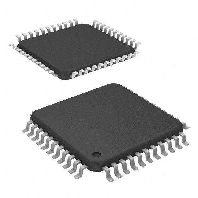
| 描述 | IC RF TX SNGL-CHIP LP 16QFN射频发射器 2.4GHz TRANSMITTER ONLY |
| 产品分类 | |
| 品牌 | Texas Instruments |
| 产品手册 | |
| 产品图片 |
|
| rohs | 符合RoHS无铅 / 符合限制有害物质指令(RoHS)规范要求 |
| 产品系列 | RF集成电路,射频发射器,Texas Instruments CC2550RST- |
| 数据手册 | |
| 产品型号 | CC2550RST |
| 产品培训模块 | http://www.digikey.cn/PTM/IndividualPTM.page?site=cn&lang=zhs&ptm=26085 |
| 产品种类 | 射频发射器 |
| 其它名称 | 296-32848-5 |
| 制造商产品页 | http://www.ti.com/general/docs/suppproductinfo.tsp?distId=10&orderablePartNumber=CC2550RST |
| 功率-输出 | -30dBm ~ 1dBm |
| 包装 | 管件 |
| 商标 | Texas Instruments |
| 天线连接器 | PCB,表面贴装 |
| 存储容量 | - |
| 安装风格 | SMD/SMT |
| 封装 | Tube |
| 封装/外壳 | 16-VQFN 裸露焊盘 |
| 封装/箱体 | VQFNP-16 |
| 工作温度 | -40°C ~ 85°C |
| 工作电源电压 | 2.5 V, 3.3 V |
| 工作频率 | 2483.5 MHz |
| 工厂包装数量 | 490 |
| 应用 | ISM,SRD |
| 数据接口 | PCB,表面贴装 |
| 数据速率(最大值) | 500 kBaud |
| 最大工作温度 | + 85 C |
| 最小工作温度 | - 40 C |
| 标准包装 | 490 |
| 特性 | - |
| 电压-电源 | 1.8 V ~ 3.6 V |
| 电流-传输 | 21.3mA @ 1 dBm |
| 类型 | Transmitter |
| 系列 | CC2550 |
| 调制或协议 | 2-FSK,ASK,GFSK,MSK,OOK |
| 配用 | /product-detail/zh/CC2500-CC2550DK/296-23077-ND/1690539/product-detail/zh/CC2550EMK/296-30821-ND/1690546 |
| 频率 | 2.4GHz |


- 商务部:美国ITC正式对集成电路等产品启动337调查
- 曝三星4nm工艺存在良率问题 高通将骁龙8 Gen1或转产台积电
- 太阳诱电将投资9.5亿元在常州建新厂生产MLCC 预计2023年完工
- 英特尔发布欧洲新工厂建设计划 深化IDM 2.0 战略
- 台积电先进制程称霸业界 有大客户加持明年业绩稳了
- 达到5530亿美元!SIA预计今年全球半导体销售额将创下新高
- 英特尔拟将自动驾驶子公司Mobileye上市 估值或超500亿美元
- 三星加码芯片和SET,合并消费电子和移动部门,撤换高东真等 CEO
- 三星电子宣布重大人事变动 还合并消费电子和移动部门
- 海关总署:前11个月进口集成电路产品价值2.52万亿元 增长14.8%


PDF Datasheet 数据手册内容提取
CC2550 CC2550 Low-Cost Low-Power 2.4 GHz RF Transmitter Applications • 2400-2483.5 MHz ISM/SRD band systems • Wireless audio • Consumer electronics • RF enabled remote controls • Wireless game controllers Product Description The CC2550 is a low-cost 2.4 GHz transmitter The main operating parameters and the 64- designed for very low-power wireless appli- byte transmit FIFO of CC2550 can be controlled cations. The circuit is intended for the 2400- via an SPI interface. In a typical system, the 2483.5 MHz ISM (Industrial, Scientific and CC2550 will be used together with a micro- Medical) and SRD (Short Range Device) freq- controller and a few passive components. uency band. The RF transmitter is integrated with a highly configurable baseband modulator. The modulator supports various modulation formats and has a configurable data rate up to 500 kBaud. The CC2550 provides extensive hardware support for packet handling, data buffering and burst transmissions. Key Features RF Performance Low-Power Features • Programmable output power up to +1 dBm • 200 nA SLEEP mode current consumption • Programmable data rate from 1.2 to 500 • Fast startup time: 240 us from SLEEP to kBaud TX mode (measured on EM design [3]) • Frequency range: 2400 – 2483.5 MHz • 64-byte TX data FIFO (enables burst mode data transmission) Analog Features General • OOK, 2-FSK, GFSK, and MSK supported • Suitable for frequency hopping and multi- • Few external components: Complete on- channel systems due to a fast settling chip frequency synthesizer, no external frequency synthesizer with 90 us settling filters needed time • Green package: RoHS compliant and no • Integrated analog temperature sensor antimony or bromine • Small size (QLP 4x4 mm package, 16 Digital Features pins) • Suited for systems compliant with EN 300 • Flexible support for packet oriented 328 and EN 300 440 class 2 (Europe), systems: On-chip support for sync word FCC CFR47 Part 15 (US), and ARIB STD- insertion, flexible packet length, and T66 (Japan) automatic CRC handling • Support for asynchronous and • Efficient SPI interface: All registers can be synchronous serial transmit mode for programmed with one “burst” transfer backwards compatibility with existing radio • Optional automatic whitening of data communication protocols SWRS039B Page 1 of 58
CC2550 Table of Contents APPLICATIONS...........................................................................................................................................1 PRODUCT DESCRIPTION.........................................................................................................................1 KEY FEATURES..........................................................................................................................................1 RF PERFORMANCE...................................................................................................................................1 ANALOG FEATURES.................................................................................................................................1 DIGITAL FEATURES..................................................................................................................................1 LOW-POWER FEATURES.........................................................................................................................1 GENERAL.....................................................................................................................................................1 TABLE OF CONTENTS..............................................................................................................................2 ABBREVIATIONS........................................................................................................................................4 1 ABSOLUTE MAXIMUM RATINGS..............................................................................................4 2 OPERATING CONDITIONS..........................................................................................................5 3 GENERAL CHARACTERISTICS..................................................................................................5 4 ELECTRICAL SPECIFICATIONS................................................................................................5 4.1 CURRENT CONSUMPTION.....................................................................................................................5 4.2 RF TRANSMIT SECTION........................................................................................................................6 4.3 CRYSTAL OSCILLATOR.........................................................................................................................7 4.4 FREQUENCY SYNTHESIZER CHARACTERISTICS.....................................................................................7 4.5 ANALOG TEMPERATURE SENSOR.........................................................................................................8 4.6 DC CHARACTERISTICS.........................................................................................................................8 4.7 POWER-ON RESET................................................................................................................................8 5 PIN CONFIGURATION...................................................................................................................9 6 CIRCUIT DESCRIPTION.............................................................................................................10 7 APPLICATION CIRCUIT.............................................................................................................10 8 CONFIGURATION OVERVIEW.................................................................................................13 9 CONFIGURATION SOFTWARE.................................................................................................14 10 4-WIRE SERIAL CONFIGURATION AND DATA INTERFACE...........................................14 10.1 CHIP STATUS BYTE............................................................................................................................15 10.2 REGISTERS ACCESS............................................................................................................................16 10.3 SPI READ...........................................................................................................................................16 10.4 COMMAND STROBES..........................................................................................................................17 10.5 FIFO ACCESS.....................................................................................................................................17 10.6 PATABLE ACCESS.............................................................................................................................17 11 MICROCONTROLLER INTERFACE AND PIN CONFIGURATION...................................18 11.1 CONFIGURATION INTERFACE..............................................................................................................18 11.2 GENERAL CONTROL AND STATUS PINS..............................................................................................18 12 DATA RATE PROGRAMMING...................................................................................................19 13 PACKET HANDLING HARDWARE SUPPORT.......................................................................19 13.1 DATA WHITENING...............................................................................................................................19 13.2 PACKET FORMAT................................................................................................................................20 13.3 PACKET HANDLING IN TRANSMIT MODE............................................................................................22 13.4 PACKET HANDLING IN FIRMWARE......................................................................................................22 14 MODULATION FORMATS..........................................................................................................22 14.1 FREQUENCY SHIFT KEYING................................................................................................................23 14.2 MINIMUM SHIFT KEYING....................................................................................................................23 14.3 AMPLITUDE MODULATION.................................................................................................................23 15 FORWARD ERROR CORRECTION WITH INTERLEAVING..............................................23 15.1 FORWARD ERROR CORRECTION (FEC)...............................................................................................23 15.2 INTERLEAVING...................................................................................................................................24 16 RADIO CONTROL.........................................................................................................................25 SWRS039B Page 2 of 58
CC2550 16.1 POWER-ON START-UP SEQUENCE......................................................................................................25 16.2 CRYSTAL CONTROL............................................................................................................................26 16.3 VOLTAGE REGULATOR CONTROL.......................................................................................................26 16.4 TX MODE...........................................................................................................................................27 16.5 TIMING...............................................................................................................................................27 17 TX FIFO...........................................................................................................................................27 18 FREQUENCY PROGRAMMING.................................................................................................28 19 VCO..................................................................................................................................................29 19.1 VCO AND PLL SELF-CALIBRATION...................................................................................................29 20 VOLTAGE REGULATORS..........................................................................................................29 21 OUTPUT POWER PROGRAMMING.........................................................................................30 22 CRYSTAL OSCILLATOR.............................................................................................................32 22.1 REFERENCE SIGNAL...........................................................................................................................32 23 EXTERNAL RF MATCH..............................................................................................................32 24 PCB LAYOUT RECOMMENDATIONS......................................................................................33 25 GENERAL PURPOSE / TEST OUTPUT CONTROL PINS......................................................33 26 ASYNCHRONOUS AND SYNCHRONOUS SERIAL OPERATION.......................................34 26.1 ASYNCHRONOUS OPERATION.............................................................................................................34 26.2 SYNCHRONOUS SERIAL OPERATION...................................................................................................35 27 SYSTEM CONSIDERATIONS AND GUIDELINES..................................................................35 27.1 SRD REGULATIONS............................................................................................................................35 27.2 FREQUENCY HOPPING AND MULTI-CHANNEL SYSTEMS.....................................................................35 27.3 WIDEBAND MODULATION NOT USING SPREAD SPECTRUM................................................................36 27.4 DATA BURST TRANSMISSIONS............................................................................................................36 27.5 CONTINUOUS TRANSMISSIONS...........................................................................................................36 27.6 SPECTRUM EFFICIENT MODULATION..................................................................................................36 27.7 LOW COST SYSTEMS..........................................................................................................................36 27.8 BATTERY OPERATED SYSTEMS..........................................................................................................36 27.9 INCREASING OUTPUT POWER.............................................................................................................37 28 CONFIGURATION REGISTERS.................................................................................................37 28.1 CONFIGURATION REGISTER DETAILS.................................................................................................41 28.2 STATUS REGISTER DETAILS................................................................................................................49 29 PACKAGE DESCRIPTION (QLP 16)..........................................................................................52 29.1 RECOMMENDED PCB LAYOUT FOR PACKAGE (QLP 16)....................................................................53 29.2 PACKAGE THERMAL PROPERTIES.......................................................................................................53 29.3 SOLDERING INFORMATION.................................................................................................................53 29.4 TRAY SPECIFICATION.........................................................................................................................54 29.5 CARRIER TAPE AND REEL SPECIFICATION..........................................................................................54 30 ORDERING INFORMATION.......................................................................................................54 31 REFERENCES................................................................................................................................54 32 GENERAL INFORMATION.........................................................................................................55 32.1 DOCUMENT HISTORY.........................................................................................................................55 32.2 PRODUCT STATUS DEFINITIONS.........................................................................................................56 33 ADDRESS INFORMATION..........................................................................................................57 34 TI WORLDWIDE TECHNICAL SUPPORT...............................................................................57 SWRS039B Page 3 of 58
CC2550 Abbreviations Abbreviations used in this data sheet are described below. ACP Adjacent Channel Power NA Not Applicable ADC Analog to Digital Converter NRZ Non Return to Zero (coding) AGC Automatic Gain Control LO Local Oscillator AMR Automatic Meter Reading OBW Occupied Bandwidth ARIB Association of Radio Industries and Businesses OOK On Off Keying ASK Amplitude Shift Keying PA Power Amplifier BER Bit Error Rate PCB Printed Circuit Board BT Bandwidth-Time product PD Power Down CFR Code of Federal Regulations PER Packet Error Rate CRC Cyclic Redundancy Check PLL Phase Locked Loop DC Direct Current POR Power-on Reset ESR Equivalent Series Resistance QPSK Quadrature Phase Shift Keying FCC Federal Communications Commission QLP Quad Leadless Package FEC Forward Error Correction RF Radio Frequency FHSS Frequency Hopping Spread Spectrum RX Receive, Receive Mode FIFO First-In-First-Out SMD Surface Mount Device 2-FSK Frequency Shift Keying SNR Signal to Noise Ratio GFSK Gaussian shaped Frequency Shift Keying SPI Serial Peripheral Interface I/Q In-Phase/Quadrature SRD Short Range Device ISM Industrial, Scientific and Medical TX Transmit, Transmit Mode LC Inductor-Capacitor VCO Voltage Controlled Oscillator LO Local Oscillator WLAN Wireless Local Area Networks MCU Microcontroller Unit XOSC Crystal Oscillator MSB Most Significant Bit XTAL Crystal MSK Minimum Shift Keying 1 Absolute Maximum Ratings Under no circumstances must the absolute maximum ratings given in Table 1 be violated. Stress exceeding one or more of the limiting values may cause permanent damage to the device. Caution! ESD sensitive device. Precaution should be used when handling the device in order to prevent permanent damage. Parameter Min Max Units Condition/Note Supply voltage –0.3 3.9 V All supply pins must have the same voltage Voltage on any digital pin –0.3 VDD+0.3, V max 3.9 Voltage on the pins RF_P, RF_N –0.3 2.0 V and DCOUPL Storage temperature range –50 150 °C Solder reflow temperature 260 °C According to IPC/JEDEC J-STD-020D ESD <500 V According to JEDEC STD 22, method A114, Human Body Model Table 1: Absolute Maximum Ratings SWRS039B Page 4 of 58
CC2550 2 Operating Conditions The CC2550 operating conditions are listed in Table 2 below. Parameter Min Max Unit Condition/Note Operating temperature –40 85 °C Operating supply voltage 1.8 3.6 V All supply pins must have the same voltage Table 2: Operating Conditions 3 General Characteristics Parameter Min Typ Max Unit Condition/Note Frequency range 2400 2483.5 MHz Data rate 1.2 500 kBaud 2-FSK 1.2 250 kBaud GFSK and OOK 26 500 kBaud (Shaped) MSK (also known as differential offset QPSK) Optional Manchester encoding (the data rate in kbps will be half the baud rate). Table 3: General Characteristics 4 Electrical Specifications 4.1 Current Consumption Tc = 25°C, VDD = 3.0 V if nothing else stated. All measurement results obtained using the CC2550EM reference design ([3]). Parameter Min Typ Max Unit Condition/Note Current consumption in power 200 nA Voltage regulator to digital part off (SLEEP state). All GDO pins down modes programmed to 0x2F (HW to o) 160 µA Voltage regulator to digital part on, all other modules in power down (XOFF state) Current consumption 1.4 mA Only voltage regulator to digital part and crystal oscillator running (IDLE state) 7.3 mA Only the frequency synthesizer is running (FSTXON state). This current consumption is also representative for the other intermediate states when going from IDLE to TX, including the calibration state. Current consumption, TX states 11.2 mA Transmit mode, –12 dBm output power 14.7 mA Transmit mode, -6 dBm output power 19.4 mA Transmit mode, 0 dBm output power 21.3 mA Transmit mode, +1 dBm output power Table 4: Current Consumption SWRS039B Page 5 of 58
CC2550 4.2 RF Transmit Section Tc = 25°C, VDD = 3.0 V, 0 dBm if nothing else stated. All measurement results obtained using the CC2550EM reference design ([3]). Parameter Min Typ Max Unit Condition/Note Differential load 80 + j74 Ω Differential impedance as seen from the RF-port (RF_P impedance and RF_N) towards the antenna. Follow the CC2550EM reference design ([3]) available from the TI website. Output power, highest +1 dBm Output power is programmable and full range is available setting across the entire frequency band. Delivered to 50 Ω single-ended load via CC2550EM reference design ([3]) RF matching network. Output power, lowest –30 dBm Output power is programmable and full range is available setting across the entire frequency band. Delivered to 50 Ω single-ended load via CC2550EM reference design ([3]) RF matching network. It is possible to program less than -30 dBm output power, but this is not recommended due to large variation in output power across operating conditions and processing corners for these settings. Adjacent channel -25 dBc 2.4 kBaud, 38.2 kHz deviation, 2-FSK, 250 kHz channel power (ACP) @2440 spacing MHz -25 dBc 10 kBaud, 38.2 kHz deviation, 2-FSK, 250 kHz channel spacing -25 dBc 250 kBaud, MSK, 750 kHz channel spacing -24 dBc 500 kBaud, MSK, 1 MHz channel spacing Spurious emissions 25 MHz – 1 GHz –36 dBm 47-74, 87.5-118, 174- –54 dBm 230, 470-862 MHz 1800-1900 MHz –47 dBm Restricted band in Europe At 2·RF and 3·RF –41 dBm Restricted bands in USA Otherwise above 1 –30 dBm GHz TX latency 8 bit Serial operation. Time from sampling the data on the transmitter data input pin until it is observed on the RF output ports. Table 5: RF Transmit Parameters SWRS039B Page 6 of 58
CC2550 4.3 Crystal Oscillator Tc = 25°C, VDD = 3.0 V if nothing else stated. All measurement results obtained using the CC2550EM reference design ([3]). Parameter Min Typ Max Unit Condition/Note Crystal frequency 26 26 27 MHz Tolerance ±40 ppm This is the total tolerance including a) initial tolerance, b) crystal loading, c) aging and d) temperature dependence. The acceptable crystal tolerance depends on RF frequency and channel spacing / bandwidth. ESR 100 Ω Start-up time 150 µs Measured on CC2500EM reference design ([3]) using crystal AT-41CD2 from NDK. This parameter is to a large degree crystal dependent. Table 6: Crystal Oscillator Parameters 4.4 Frequency Synthesizer Characteristics Tc = 25°C, VDD = 3.0 V if nothing else stated. All measurement results obtained using the CC2550EM reference design ([3]). Min figures are given using a 27 MHz crystal. Typ and max figures are given using a 26 MHz crystal. Parameter Min Typ Max Unit Condition/Note Programmed 397 F / 427 Hz 26-27 MHz crystal. XOSC frequency resolution 216 Synthesizer frequency ±40 ppm Given by crystal used. Required accuracy (including tolerance temperature and aging) depends on frequency band and channel bandwidth / spacing. RF carrier phase noise –74 dBc/Hz @ 50 kHz offset from carrier @2440 MHz –74 dBc/Hz @ 100 kHz offset from carrier –77 dBc/Hz @ 200 kHz offset from carrier –97 dBc/Hz @ 1 MHz offset from carrier –106 dBc/Hz @ 2 MHz offset from carrier –114 dBc/Hz @ 5 MHz offset from carrier –117 dBc/Hz @ 10 MHz offset from carrier PLL turn-on / hop time 85.1 88.4 88.4 µs Time from leaving the IDLE state until arriving in the FSTXON or TX state, when not performing calibration. Crystal oscillator running. PLL calibration time 694 721 721 µs Calibration can be initiated manually or automatically before entering or after leaving RX/TX. Table 7: Frequency Synthesizer Parameters SWRS039B Page 7 of 58
CC2550 4.5 Analog Temperature Sensor The characteristics of the analog temperature sensor at 3.0 V supply voltage are listed in Table 8 below. Note that it is necessary to write 0xBF to the PTEST register to use the analog temperature sensor in the IDLE state. Parameter Min Typ Max Unit Condition/Note Output voltage at –40°C 0.660 V Output voltage at 0°C 0.755 V Output voltage at +40°C 0.859 V Output voltage at +80°C 0.958 V Temperature coefficient 2.54 mV/°C Fitted from –20°C to +80°C Error in calculated -2 * 0 2 * °C From –20°C to +80°C when using 2.54 mV / °C, temperature, calibrated after 1-point calibration at room temperature * The indicated minimum and maximum error with 1- point calibration is based on simulated values for typical process parameters Current consumption 0.3 mA increase when enabled Table 8: Analog Temperature Sensor Parameters 4.6 DC Characteristics Tc = 25°C if nothing else stated. Digital Inputs/Outputs Min Max Unit Condition/Note Logic "0" input voltage 0 0.7 V Logic "1" input voltage VDD-0.7 VDD V Logic "0" output voltage 0 0.5 V For up to 4 mA output current Logic "1" output voltage VDD-0.3 VDD V For up to 4 mA output current Logic "0" input current NA -50 nA Input equals 0 V Logic "1" input current NA 50 nA Input equals VDD Table 9: DC Characteristics 4.7 Power-On Reset When the power supply complies with the requirements in Table 10 below, proper Power-On- Reset functionality is guaranteed. Otherwise, the chip should be assumed to have unknown state until transmitting an SRES strobe over the SPI interface. See Section 16.1 on page 25 for further details. Parameter Min Typ Max Unit Condition/Note Power-up ramp-up time 5 ms From 0 V until reaching 1.8 V Power off time 1 ms Minimum time between power off and power-on. Table 10: Power-on Reset Requirements SWRS039B Page 8 of 58
CC2550 5 Pin Configuration D R SI DGUA RBIAS AVDD 16 15 14 13 SCLK1 12AVDD SO (GDO1)2 11RF_N DVDD3 10RF_P DCOUPL4 9 CSn GND 5 6 7 8 Exposed die X A X G O V O D attach pad S D S O C D C 0 _Q _Q (A 1 2 TE S T ) Figure 1: Pinout Top View Note: The exposed die attach pad must be connected to a solid ground plane as this is the main ground connection for the chip. Pin # Pin Name Pin Type Description 1 SCLK Digital Input Serial configuration interface, clock input 2 SO (GDO1) Digital Output Serial configuration interface, data output. Optional general output pin when CSn is high 3 DVDD Power (Digital) 1.8 - 3.6 V digital power supply for digital I/O’s and for the digital core voltage regulator 4 DCOUPL Power (Digital) 1.6 - 2.0 V digital power supply output for decoupling. NOTE: This pin is intended for use with the CC2550 only. It can not be used to provide supply voltage to other devices. 5 XOSC_Q1 Analog I/O Crystal oscillator pin 1, or external clock input 6 AVDD Power (Analog) 1.8 - 3.6 V analog power supply connection 7 XOSC_Q2 Analog I/O Crystal oscillator pin 2 8 GDO0 Digital I/O Digital output pin for general use: (ATEST) • Test signals • FIFO status signals • Clock output, down-divided from XOSC • Serial input TX data Also used as analog test I/O for prototype/production testing 9 CSn Digital Input Serial configuration interface, chip select 10 RF_P RF Output Positive RF output signal from PA 11 RF_N RF Output Negative RF output signal from PA 12 AVDD Power (Analog) 1.8 - 3.6 V analog power supply connection 13 AVDD Power (Analog) 1.8 - 3.6 V analog power supply connection 14 RBIAS Analog I/O External bias resistor for reference current 15 DGUARD Power (Digital) Power supply connection for digital noise isolation 16 SI Digital Input Serial configuration interface, data input Table 11: Pinout Overview SWRS039B Page 9 of 58
CC2550 6 Circuit Description RADIO CONTROL R R SCLK RRFF__NP PA SFYRNETQH ODULATO FEC /TERLEAVE PACKETHANDLER TX FIFO DIGITALNTERFACETO MCU SSCOISn (GDO1) BIAS XOSC M N I GDO0 (ATEST) I RBIAS XOSC_Q1 XOSC_Q2 Figure 2: CC2550 Simplified Block Diagram A simplified block diagram of CC2550 is shown XOSC_Q2. The crystal oscillator generates the in Figure 2. reference frequency for the synthesizer, as well as clocks for the digital part. The CC2550 transmitter is based on direct synthesis of the RF frequency. A 4-wire SPI serial interface is used for configuration and data buffer access. The frequency synthesizer includes a completely on-chip LC VCO. The digital baseband includes support for channel configuration, packet handling and A crystal is to be connected to XOSC_Q1 and data buffering. 7 Application Circuit Only a few external components are required The balun and LC filter component values and for using the CC2550. The recommended their placement are important to keep the application circuit is shown in Figure 3. The performance optimized. It is highly external components are described in Table recommended to follow the CC2550EM 12, and typical values are given in Table 13. reference design ([3]). Bias resistor Crystal The bias resistor R141 is used to set an The crystal oscillator uses an external crystal accurate bias current. with two loading capacitors (C51 and C71). See Section 22 on page 32 for details. Balun and RF matching Power supply decoupling The components between the RF_N/RF_P pins and the point where the two signals are joined The power supply must be properly decoupled together (C102, C112, L101, and L111) form a close to the supply pins. Note that decoupling balun that converts the differential RF signal capacitors are not shown in the application on CC2550 to a single-ended RF signal. C101 circuit. The placement and the size of the and C111 are needed for DC blocking. decoupling capacitors are very important to Together with an appropriate LC network, the achieve the optimum performance. The balun components also transform the CC2550EM reference design ([3]) should be followed closely. impedance to match a 50 Ω antenna (or cable). Suggested values are listed in Table 13. SWRS039B Page 10 of 58
CC2550 Component Description C41 Decoupling capacitor for on-chip voltage regulator to digital part C51/C71 Crystal loading capacitors, see Section 22 on page 32 for details C101/C111 RF balun DC blocking capacitors C102/C112 RF balun/matching capacitors C103/C104 RF LC filter/matching capacitors L101/L111 RF balun/matching inductors (inexpensive multi-layer type) L102 RF LC filter inductor (inexpensive multi-layer type) R141 Resistor for internal bias current reference XTAL 26-27 MHz crystal, see Section 22 on page 32 for details Table 12: Overview of External Components (excluding supply decoupling capacitors) 1.8V-3.6V power supply R141 SI Antenna SI 16 RD 15 AS 14 AVDD13 (50 Ohm) ce SCLK 1 SCLK GUA RBI AVDD 12 L111 ntefa S(GODO1) 2 SO (GDOC1)CD2550RF_N 11 C111 C112 Digital I C41 34 DDCVODUDPD5L XOSC_Q1IE AT6 AVDDTAC7 XOSC_Q2H PA8 GDO0D:RFC_PS n1 09 C101 C1L01201 C1L01302 C104 Alternative: GDO0 Folded dipole PCB (optional) antenna (no external CSn components needed) XTAL C51 C71 Figure 3: Typical Application and Evaluation Circuit (excluding supply decoupling capacitors) SWRS039B Page 11 of 58
CC2550 Component Value Manufacturer C41 100 nF±10%, 0402 X5R Murata GRM15 series C51 27 pF±5%, 0402 NP0 Murata GRM15 series C71 27 pF±5%, 0402 NP0 Murata GRM15 series C101 100 pF±5%, 0402 NP0 Murata GRM15 series C102 1.0 pF±0.25pF, 0402 NP0 Murata GRM15 series C103 1.8 pF±0.25pF, 0402 NP0 Murata GRM15 series C104 1.5 pF±0.25pF, 0402 NP0 Murata GRM15 series C111 100 pF±5%, 0402 NP0 Murata GRM15 series C112 1.0 pF±0.25pF, 0402 NP0 Murata GRM15 series L101 1.2 nH±0.3nH, 0402 monolithic Murata LQG15 series L102 1.2 nH±0.3nH, 0402 monolithic Murata LQG15 series L111 1.2 nH±0.3nH, 0402 monolithic Murata LQG15 series R141 56 kΩ±1%, 0402 Koa RK73 series XTAL 26.0 MHz surface mount crystal NDK, AT-41CD2 Table 13: Bill of Materials for the Application Circuit Measurements have been performed with The Gerber files for the CC2550EM reference multi-layer inductors from other manufacturers design ([3]) are available from the TI website. (e.g. Würth) and the measurement results were the same as when using the Murata part. SWRS039B Page 12 of 58
CC2550 8 Configuration Overview CC2550 can be configured to achieve optimum • Forward Error Correction (FEC) with performance for many different applications. interleaving Configuration is done using the SPI interface. • Data Whitening The following key parameters can be programmed: Details of each configuration register can be • Power-down / power up mode found in Section 28, starting on page 37. • Crystal oscillator power-up / power – down Figure 4 shows a simplified state diagram that • Transmit mode explains the main CC2550 states, together with • RF channel selection typical usage and current consumption. For • Data rate detailed information on controlling the CC2550 • Modulation format state machine, and a complete state diagram, • RF output power see Section 16, starting on page 25. • Data buffering with 64-byte transmit FIFO • Packet radio hardware support Figure 4: Simplified State Diagram with Typical Current Consumption SWRS039B Page 13 of 58
CC2550 9 Configuration Software CC2550 can be configured using the SmartRF® After chip reset, all the registers have default Studio software ([4]). The SmartRF® Studio values as shown in the tables in Section 28. software is highly recommended for obtaining The optimum register setting might differ from optimum register settings, and for evaluating the default value. After a reset all registers that performance and functionality. A screenshot of shall be different from the default value the SmartRF® Studio user interface for CC2550 therefore needs to be programmed through the is shown in Figure 5. SPI interface. Figure 5: SmartRF® Studio [4] User Interface 10 4-wire Serial Configuration and Data Interface CC2550 is configured via a simple 4-wire SPI- cancelled. The timing for the address and data compatible interface (SI, SO, SCLK and CSn) transfer on the SPI interface is shown in Figure where CC2550 is the slave. This interface is 6 with reference to Table 14. also used to write buffered data. All transfer on When CSn is pulled low, the MCU must wait the SPI interface are done most significant bit until CC2500 SO pin goes low before starting to first. transfer the header byte. This indicates that All transactions on the SPI interface start with the crystal is running. Unless the chip was in a header byte containing a R/W bit, a burst the SLEEP or XOFF states, the SO pin will access bit (B), and a 6-bit address (A5 – A0). always go low immediately after taking CSn low. The CSn pin must be kept low during transfers on the SPI bus. If CSn goes high during the transfer of a header byte or during read/write from/to a register, the transfer will be SWRS039B Page 14 of 58
CC2550 t t t t t t sp ch cl sd hd ns SCLK: CSn: Write to register: SI X 0 B A5 A4 A3 A2 A1 A0 X DW7 DW6 DW5 DW4 DW3 DW2 DW1 DW0 X SO Hi-Z S7 B S5 S4 S3 S2 S1 S0 S7 S6 S5 S4 S3 S2 S1 S0 Hi-Z Read from register: SI X 1 B A5 A4 A3 A2 A1 A0 X SO Hi-Z S7 B S5 S4 S3 S2 S1 S0 DR7 DR6 DR5 DR4 DR3 DR2 DR1 DR0 Hi-Z Figure 6: Configuration Registers Write and Read Operations Parameter Description Min Max Units fSCLK SCLK frequency - 10 MHz 100 ns delay inserted between address byte and data byte (single access), or between address and data, and between each data byte (burst access). SCLK frequency, single access 9 MHz No delay between address and data byte SCLK frequency, burst access 6.5 MHz No delay between address and data byte, or between data bytes tsp,pd CSn low to positive edge on SCLK, in power-down mode 150 - µs tsp CSn low to positive edge on SCLK, in active mode 20 - ns t Clock high 50 - ns ch t Clock low 50 - ns cl t Clock rise time - 5 ns rise t Clock fall time - 5 ns fall tsd Setup data (negative SCLK edge) to Single access 55 - ns positive edge on SCLK Burst access 76 - ns (btesdt waepepnlie dsa btae tbwyeteesn) ad dress and data bytes, and thd Hold data after positive edge on SCLK 20 - ns tns Negative edge on SCLK to CSn high 20 - ns Table 14: SPI Interface Timing Requirements Note: The minimum t figure in Table 14 can be used in cases where the user does not read the sp,pd CHIP_RDYn signal. CSn low to positive edge on SCLK when the chip is woken from power-down depends on the start-up time of the crystal being used. The 150 us in Table 14 is the crystal oscillator start-up time measured on CC2550EM reference design ([3]) using crystal AT-41CD2 from NDK. 10.1 Chip Status Byte before the first positive edge of SCLK. The CHIP_RDYn signal indicates that the crystal is When the header byte, data byte, or command running. strobe is sent on the SPI interface, the chip status byte is sent by the CC2550 on the SO Bits 6, 5, and 4 comprise the STATE value. pin. The status byte contains key status This value reflects the state of the chip. The signals, useful for the MCU. The first bit, s7, is XOSC and power to the digital core is on in the the CHIP_RDYn signal; this signal must go low IDLE state, but all other modules are in power SWRS039B Page 15 of 58
CC2550 down. The frequency and channel contains the number of bytes that can be configuration should only be updated when the written to the TX FIFO. When chip is in this state. The TX state is active FIFO_BYTES_AVAILABLE=15, 15 or more when the chip is transmitting. bytes are available/free. The last four bits (3:0) in the status byte Table 15 gives a status byte summary. contains FIFO_BYTES_AVAILABLE. For write operations (the R/W bit in the header byte is set to 0), the FIFO_BYTES_AVAILABLE field Bits Name Description 7 CHIP_RDYn Stays high until power and crystal have stabilized. Should always be low when using the SPI interface. 6:4 STATE[2:0] Indicates the current main state machine mode Value State Description 000 IDLE Idle state (Also reported for some transitional states instead of SETTLING or CALIBRATE) 001 Not used 010 TX Transmit mode 011 FSTXON Frequency synthesizer is on, ready to start transmitting 100 CALIBRATE Frequency synthesizer calibration is running 101 SETTLING PLL is settling 110 Not used 111 TXFIFO_UNDERFLOW TX FIFO has underflowed. Acknowledge with SFTX 3:0 FIFO_BYTES_AVAILABLE[3:0] The number of free bytes in the TX FIFO (the R/W bit in the header byte must be set to 0) Table 15: Status Byte Summary 10.2 Registers Access burst bit (B) in the header byte. The address bits (A – A ) sets the start address in an The configuration registers on the CC2550 are 5 0 internal address counter. This counter is located on SPI addresses from 0x00 to 0x2E. incremented by one each new byte (every 8 Table 24 on page 39 lists all configuration clock pulses). The burst access is either a registers. It is highly recommended to use read or a write access and must be terminated SmartRF® Studio [4] to generate optimum by setting CSn high. register settings. The detailed description of each register is found in Section 28.1, starting For register addresses in the range 0x30- on page 41. All configuration registers can be 0x3D, the burst bit is used to select between both written to and read. The R/W bit controls status registers, burst bit is one, and command if the register should be written to or read. strobes, burst bit is zero (see Section 10.4 When writing to registers, the status byte is below). Because of this, burst access is not sent on the SO pin each time a header byte or available for status registers and they must be data byte is transmitted on the SI pin. When accessed one at a time. The status registers reading from registers, the status byte is sent can only be read. on the SO pin each time a header byte is transmitted on the SI pin. 10.3 SPI Read Registers with consecutive addresses can be When reading register fields over the SPI accessed in an efficient way by setting the interface while the register fields are updated SWRS039B Page 16 of 58
CC2550 by the radio hardware (e.g. MARCSTATE or one header byte and then consecutive data TXBYTES), there is a small, but finite, bytes until terminating the access by setting probability that a single read from the register CSn high. is being corrupt. As an example, the probability The following header bytes access the FIFO: of any single read from TXBYTES being corrupt, assuming the maximum data rate is • 0x3F: Single byte access to TX FIFO used, is approximately 80 ppm. Refer to the • 0x7F: Burst access to TX FIFO CC2550 Errata Note [1] for more details. 10.4 Command Strobes When writing to the TX FIFO, the status byte (see Section 10.1) is output for each new data Command strobes may be viewed as single byte on SO, as shown in Figure 6. This status byte instructions to CC2550. By addressing a byte can be used to detect TX FIFO underflow command strobe register, internal sequences while writing data to the TX FIFO. Note that will be started. These commands are used to the status byte contains the number of bytes disable the crystal oscillator, enable transmit free before writing the byte in progress to the mode, flush the TX FIFO etc. The 9 command TX FIFO. When the last byte that fits in the TX strobes are listed in Table 23 on page 38. FIFO is transmitted on SI, the status byte The command strobe registers are accessed received concurrently on SO will indicate that by transferring a single header byte (no data is one byte is free in the TX FIFO. being transferred). That is, only the R/W bit, The TX FIFO may be flushed by issuing a the burst access bit (set to 0), and the six SFTX command strobe. A SFTX command address bits (in the range 0x30 through 0x3D) strobe can only be issued in the IDLE or are written. TX_UNDERFLOW states. The TX FIFO is When writing command strobes, the status flushed when going to the SLEEP state. byte is sent on the SO pin. Figure 8 gives a brief overview of different A command strobe may be followed by any register access types possible. other SPI access without pulling CSn high. However, if an SRES strobe is being issued, 10.6 PATABLE Access one will have to wait for SO to go low again before the next header byte can be issued as The 0x3E address is used to access the shown in Figure 7. The command strobes are PATABLE, which is used for selecting PA executed immediately, with the exception of power control settings. The PATABLE is an 8- the SPWD and the SXOFF strobes that are byte table, but not all entries into this table are executed when CSn goes high. used. The entries to use are selected by the 3- bit value FREND0.PA_POWER. • When using 2-FSK, GFSK, or MSK modulation only the first entry into this table is used (index 0). • When using OOK modulation the first two entries into this table are used (index 0 Figure 7: SRES Command Strobe and index 1). 10.5 FIFO Access Since the PATABLE is an 8-byte table, the The 64-byte TX FIFO is accessed through the table is written and read from the lowest 0x3F address and is write-only. setting (0) to the highest (7), one byte at a The burst bit is used to determine if the FIFO time. An index counter is used to control the access is a single byte access or a burst access to the table. This counter is access. The single byte access method incremented each time a byte is read or written expects a header byte with the burst bit set to to the table, and set to the lowest index when zero and one data byte. After the data byte a CSn is high. When the highest value is new header byte is expected; hence, CSn can reached the counter restarts at 0. remain low. The burst access method expects SWRS039B Page 17 of 58
CC2550 The access to the PATABLE is either single Note that the content of the PATABLE is lost byte or burst access depending on the burst when entering the SLEEP state. bit. When using burst access the index counter See Section 21 on page 30 for output power will count up; when reaching 7 the counter will programming details. restart at 0. The R/W bit controls whether the access is a write access (R/W=0) or a read access (R/W=1). If one byte is written to the PATABLE and this value is to be read out then CSn must be set high before the read access in order to set the index counter back to zero. Figure 8: Register Access Types 11 Microcontroller Interface and Pin Configuration In a typical system, CC2550 will interface to a SO pin in the SPI interface. The default setting microcontroller. This microcontroller must be for GDO1/SO is 3-state output. By selecting able to: any other of the programming options the GDO1/SO pin will become a generic pin. When • Program CC2550 into different modes CSn is low, the pin will always function as a • Write buffered data normal SO pin. • Read back status information via the 4-wire In the synchronous and asynchronous serial SPI-bus configuration interface (SI, SO, modes, the GDO0 pin is used as a serial TX SCLK and CSn) data input pin while in transmit mode. The GDO0 pin can also be used for an on-chip 11.1 Configuration Interface analog temperature sensor. By measuring the voltage on the GDO0 pin with an external ADC, The microcontroller uses four I/O pins for the the temperature can be calculated. SPI configuration interface (SI, SO, SCLK and Specifications for the temperature sensor are CSn). The SPI is described in Section 14 on found in Section 4.5 on page 8. page 14. With default PTEST register setting (0x7F) the temperature sensor output is only available 11.2 General Control and Status Pins when the frequency synthesizer is enabled The CC2550 has one dedicated configurable (e.g. the MANCAL, FSTXON and TX states). pin (GDO0) and one shared pin (GDO1) that can It is necessary to write 0xBF to the PTEST output internal status information useful for register to use the analog temperature sensor control software. These pins can be used to in the IDLE state. Before leaving the IDLE generate interrupts on the MCU. See Section state, the PTEST register should be restored to 25 page 33 for more details of the signals that its default value (0x7F). can be programmed. GDO1 is shared with the SWRS039B Page 18 of 58
CC2550 12 Data Rate Programming The data rate used when transmitting is If DRATE_M is rounded to the nearest integer programmed by the MDMCFG3.DRATE_M and and becomes 256, increment DRATE_E and the MDMCFG4.DRATE_E configuration use DRATE_M=0. registers. The data rate is given by the formula The data rate can be set from 1.2 kBaud to below. As the formula shows, the programmed 500 kBaud with a minimum step size of: data rate depends on the crystal frequency. (256+DRATE_M)⋅2DRATE_E Data Rate Typical Data Rate Data Rate R = ⋅ f Start Data Rate Stop Step Size DATA 228 XOSC [kBaud] [kBaud] [kBaud] [kBaud] 0.8 1.2/2.4 3.17 0.0062 3.17 4.8 6.35 0.0124 The following approach can be used to find suitable values for a given data rate: 6.35 9.6 12.7 0.0248 12.7 19.6 25.4 0.0496 25.4 38.4 50.8 0.0992 ⎢ ⎛R ⋅220 ⎞⎥ DRATE_E = ⎢log ⎜ DATA ⎟⎥ 50.8 76.8 101.6 0.1984 ⎢⎣ 2⎜⎝ fXOSC ⎟⎠⎥⎦ 101.6 153.6 203.1 0.3967 R ⋅228 203.1 250 406.3 0.7935 DRATE_M = DATA −256 f ⋅2DRATE_E 406.3 500 500 1.5869 XOSC Table 16: Data Rate Step Size 13 Packet Handling Hardware Support The CC2550 has built-in hardware support for • Whitening of the data with a PN9 packet oriented radio protocols. sequence. • Forward error correction by the use of In transmit mode, the packet handler can be interleaving and coding of the data configured to add the following elements to the (convolutional coding). packet stored in the TX FIFO: • A programmable number of preamble Note that register fields that control the packet bytes handling features should only be altered when • A two byte synchronization (sync) word. CC2550 is in the IDLE state. Can be duplicated to give a 4-byte sync word. It is not possible to only insert 13.1 Data whitening preamble or only insert a sync word. • A CRC checksum computed over the data From a radio perspective, the ideal over the air field. data are random and DC free. This results in the smoothest power distribution over the occupied bandwidth. This also gives the In a system where CC2550 is used as the regulation loops in the receiver uniform transmitter and CC2500 as the receiver, the operation conditions (no data dependencies). recommended setting is 4-byte preamble and 4-byte sync word, except for 500 kBaud data Real world data often contain long sequences rate where the recommended preamble length of zeros and ones. Performance can then be is 8 bytes. improved by whitening the data before transmitting, and de-whitening the data in the In addition, the following can be implemented receiver. With CC2550, in combination with a on the data field and the optional 2-byte CRC CC2500 at the receiver end, this can be done checksum: automatically by setting PKTCTRL0 SWRS039B Page 19 of 58
CC2550 .WHITE_DATA=1. All data, except the the whitening is reversed, and the original data preamble and the sync word, are then XOR-ed appear in the receiver. The PN9 sequence is with a 9-bit pseudo-random (PN9) sequence reset to all 1’s. before being transmitted as shown in Figure 9. Data whitening can only be used when At the receiver end, the data are XOR-ed with PKTCTRL0.CC2400_EN=0 (default). the same pseudo-random sequence. This way, Figure 9: Data Whitening in TX Mode 13.2 Packet Format • Synchronization word • Optional length byte The format of the data packet can be • Optional address byte configured and consists of the following items • Payload (see Figure 10): • Optional 2 byte CRC • Preamble Optional data whitening Optionally FEC encoded/decoded Legend: Optional CRC-16 calculation Inserted automatically in TX, processed and removed in RX. P(1r0e1a0m..b.1le0 b1i0ts) Sync word Length field Address field Data field CRC-16 OpUrnpoptcioreonscasele sudss ebedur -tup nsroeotrv irddeaemtdao f(vieaelpdda sirn pt RrfroXoc.mes FseEdC in TX, and/or whitening) 8 8 8 x n bits 16/32 bits 8 x n bits 16 bits bits bits Figure 10: Packet Format The preamble pattern is an alternating bytes has been transmitted, the modulator will sequence of ones and zeros (101010101…). send the sync word and then data from the TX The minimum length of the preamble is FIFO if data is available. If the TX FIFO is programmable. When enabling TX, the empty, the modulator will continue to send modulator will start transmitting the preamble. preamble bytes until the first byte is written to When the programmed number of preamble the TX FIFO. The modulator will then send the SWRS039B Page 20 of 58
CC2550 sync word and then the data bytes. The Note that the minimum packet length number of preamble bytes is programmed with supported (excluding the optional length byte the MDMCFG1.NUM_PREAMBLE value. and CRC) is one byte of payload data. The synchronization word is a two-byte value 13.2.1 Packet Length > 255 set in the SYNC1 and SYNC0 registers. A one- byte sync word can be emulated by setting the Reprogramming the packet automation control SYNC1 value to the preamble pattern. It is also register, PCKCTRL0, during TX mode opens possible to emulate a 32 bit sync word by the possibility to transmit packets that are using MDMCFG2.SYNC_MODE=3 or 7. The sync longer than 256 bytes and still be able to use word will then be repeated twice. the packet handling hardware support. At the start of the packet, the infinite packet length CC2550 supports both fixed packet length mode (PCKCTRL0.LENGTH_CONFIG=2) must protocols and variable packet length protocols. be active. The PKTLEN register is set to Variable or fixed packet length mode can be mod(length, 256). When less than 256 bytes used for packets up to 255 bytes. For longer remains of the packet the MCU disables packets, infinite packet length mode must be infinite packet length mode and activates fixed used. packet length mode. When the internal byte Fixed packet length mode is selected by counter reaches the PKTLEN value, the setting PKTCTRL0.LENGTH_CONFIG=0. The transmission ends the radio enters the state desired packet length is set by the PKTLEN determined by TXOFF_MODE). Automatic CRC register. appending can be used (by setting PKTCTRL0.CRC_EN=1). In variable packet length mode, PKTCTRL0.LENGTH_CONFIG=1, the packet When for example a 600-byte packet is to be length is configured by the first byte after the transmitted, the MCU should do the following sync word. The packet length is defined as the (see also Figure 11): payload data, excluding the length byte and • Set PKTCTRL0.LENGTH_CONFIG=2. the optional automatic CRC. • Pre-program the PKTLEN register to With PKTCTRL0.LENGTH_CONFIG=2, the mod(600,256)=88. packet length is set to infinite and transmission will continue until turned off manually. As • Transmit at least 345 bytes (600 – 255), described in the next section, this can be used for example by filling the 64-byte TX FIFO to support packet formats with different length six times (384 bytes transmitted). configuration than natively supported by CC2550. One should make sure that TX mode • Set PKTCTRL0.LENGTH_CONFIG=0. is not turned off during the transmission of the • The transmission ends when the packet first half of any byte. Refer to the CC2550 counter reaches 88. A total of 600 bytes Errata Notes [1] for more details. are transmitted. Figure 11: Packet Length > 255 SWRS039B Page 21 of 58
CC2550 13.3 Packet Handling in Transmit Mode the TX FIFO needs to be refilled while in TX. This means that the MCU needs to know the The payload that is to be transmitted must be number of bytes that can be written to TX written into the TX FIFO. The first byte written FIFO. There are two possible solutions to get must be the length byte when variable packet the necessary status information: length is enabled. The length byte has a value equal to the payload of the packet (including a) Interrupt driven solution the optional address byte). If fixed packet It is possible to use one of the GDO pins to give length is enabled, then the first byte written to an interrupt when a sync word has been the TX FIFO is interpreted as the destination transmitted and/or when a complete packet address, if this feature is enabled in the device has been transmitted (IOCFGx=0x06). In that receives the packet. addition, there are 2 configurations for the The modulator will first send the programmed IOCFGx register that are associated with the number of preamble bytes. If data is available TX FIFO (IOCFGx=0x02 and IOCFG=0x03) in the TX FIFO, the modulator will send the that can be used as interrupt sources to two-byte (optionally 4-byte) sync word and provide information on how many bytes are in then the payload in the TX FIFO. If CRC is the TX FIFO. See Table 22. enabled, the checksum is calculated over all the data pulled from the TX FIFO and the b) SPI polling result is sent as two extra bytes at the end of The PKTSTATUS register can be polled at a the payload data. If the TX FIFO runs empty given rate to get information about the current before the complete packet has been GDO0 value. The TXBYTES register can be transmitted, the radio will enter polled at a given rate to get information about TXFIFO_UNDERFLOW state. The only way to the number of bytes in the TX FIFO. exit this state is by issuing an SFTX strobe. Alternatively, the number of bytes in the TX Writing to the TX FIFO after it has underflowed FIFO can be read from the chip status byte will not restart TX mode. returned on the MISO line each time a header If whitening is enabled, everything following byte, data byte, or command strobe is sent on the sync words will be whitened. This is done the SPI bus. This only valid when R/W = 0. before the optional FEC/Interleaver stage. As explained in Section 10.3 and the CC2550 Whitening is enabled by setting Errata Notes [1], when using SPI polling there PKTCTRL0.WHITE_DATA=1. is a small, but finite, probability that a single If FEC/Interleaving is enabled, everything read from registers PKTSTATUS and TXBYTES following the sync words will be scrambled by is being corrupt. The same is the case when the interleaver, and FEC encoded before being reading the chip status byte. It is therefore modulated. FEC is enabled by setting recommended to employ an interrupt driven MDMCFG.FEC_EN=1. solution. Refer to the TI website for SW examples ([5] 13.4 Packet Handling in Firmware and [6]). When implementing a packet oriented radio protocol in firmware, the MCU needs to know when a packet has been transmitted. Additionally, for packets longer than 64 bytes 14 Modulation Formats CC2550 supports amplitude, frequency and Manchester encoding is not supported at the phase shift modulation formats. The desired same time as using the FEC/Interleaver modulation format is set in the option. MDMCFG2.MOD_FORMAT register. Optionally, the data stream can be Manchester coded by the modulator. This option is enabled by setting MDMCFG2.MANCHESTER_EN=1. SWRS039B Page 22 of 58
CC2550 14.1 Frequency Shift Keying 14.2 Minimum Shift Keying 2-FSK can optionally be shaped by a When using MSK1, the complete transmission Gaussian filter with BT=1, producing a GFSK (preamble, sync word and payload) will be modulated signal. MSK modulated. The frequency deviation is programmed with Phase shifts are performed with a constant the DEVIATION_M and DEVIATION_E values transition time. in the DEVIATN register. The value has an The fraction of a symbol period used to exponent/mantissa form, and the resultant change the phase can be modified with the deviation is given by: DEVIATN.DEVIATION_M setting. This is equivalent to changing the shaping of the symbol. f f = xosc ⋅(8+DEVIATION _M)⋅2DEVIATION_E dev 217 The MSK modulation format implemented in CC2550 inverts the sync word and data compared to e.g. signal generators. The symbol encoding is shown in Table 17. Format Symbol Coding 14.3 Amplitude Modulation 2-FSK\GFSK ‘0’ – Deviation The supported amplitude modulation On-Off Keying (OOK) simply turns on or off the PA to ‘1’ + Deviation modulate 1 and 0 respectively. Table 17: Symbol Encoding for 2-FSK/GFSK Modulation 1 Identical to offset QPSK with half-sine shaping (data coding may differ) 15 Forward Error Correction with Interleaving 15.1 Forward Error Correction (FEC) transient and time-varying phenomena will produce occasional errors even in otherwise CC2550 has built in support for Forward Error good reception conditions. FEC will mask such Correction (FEC) that can be used with CC2500 errors and, combined with interleaving of the [9] at the receiver end. To enable this option, coded data, even correct relatively long set MDMCFG1.FEC_EN=1. FEC is employed on periods of faulty reception (burst errors). the data field and CRC word in order to reduce the gross bit error rate when operating near The FEC scheme adopted for CC2550 is the sensitivity limit. Redundancy is added to convolutional coding, in which n bits are the transmitted data in such a way that the generated based on k input bits and the m CC2500 [9] can restore the original data in the most recent input bits, forming a code stream presence of some bit errors. able to withstand a certain number of bit errors between each coding state (the m-bit window). The use of FEC allows correct reception at a lower SNR, thus extending communication The convolutional coder is a rate 1/2 code with range. Alternatively, for a given SNR, using a constraint length of m=4. The coder codes FEC decreases the bit error rate (BER). As the one input bit and produces two output bits; packet error rate (PER) is related to BER by: hence, the effective data rate is halved. I.e. to transmit at the same effective data rate when using FEC, it is necessary to use twice as high over-the-air data rate. I.e. to transmit at the PER =1−(1−BER)packet_length same effective data rate when using FEC, it is necessary to use twice as high over-the-air data rate. This will require a higher CC2500 [9] a lower BER can be used to allow longer receiver bandwidth, and thus reduced packets, or a higher percentage of packets of sensitivity. In other words, the improved a given length, to be transmitted successfully. reception by using FEC and the degraded Finally, in realistic ISM radio environments, SWRS039B Page 23 of 58
CC2550 sensitivity from a higher receiver bandwidth into the rows of the matrix, whereas the data will be counteracting factors. passed onto the convolutional decoder is read from the columns of the matrix. 15.2 Interleaving When FEC and interleaving is used at least one extra byte is required for trellis Data received through radio channels will often termination. In addition, the amount of data experience burst errors due to interference transmitted over the air must be a multiple of and time-varying signal strengths. In order to the size of the interleaver buffer (two bytes). increase the robustness to errors spanning The packet control hardware therefore multiple bits, interleaving is used when FEC is automatically inserts one or two extra bytes at enabled. After de-interleaving on the receiver the end of the packet, so that the total length side, a continuous span of errors in the of the data to be interleaved is an even received stream will become single errors number. Note that these extra bytes are spread apart. invisible to the user, as they are removed CC2550 employs matrix interleaving, which is before the received packet enters the RX FIFO illustrated in Figure 12. The on-chip in a CC2500 [9]. interleaving buffer is a 4 x 4 matrix. The data When FEC and interleaving is used the bits from the rate ½ convolutional coder are minimum data payload is 2 bytes. written into the rows of the matrix, whereas the bit sequence to be transmitted is read from the Note that for the CC2500 [9] transceiver FEC is columns of the matrix. Conversely, in a CC2500 only supported in fixed packet length mode [9] receiver, the received symbols are written (PKTCTRL0.LENGTH_CONFIG=0). Interleaver Interleaver Write buffer Read buffer Packet FEC Modulator Engine Encoder Figure 12: General Principle of Matrix Interleaving SWRS039B Page 24 of 58
CC2550 16 Radio Control SIDLE SLEEP CAL_COMPLETE SPWD 0 MANCAL IDLE CSn = 0 3,4,5 1 SXOFF SCAL CSn = 0 STX | SFSTXON XOFF 2 FS_WAKEUP 6,7 FS_AUTOCAL = 01 & STX | SFSTXON FS_AUTOCAL = 00 | 10 | 11 & CALIBRATE STX | SFSTXON 8 CAL_COMPLETE SETTLING 9,10,11 SFSTXON FSTXON 18 STX STX TXOFF_MODE = 01 TX TXOFF_MODE = 10 19,20 TXFIFO_UNDERFLOW TXOFF_MODE = 00 & FS_AUTOCAL = 10 | 11 TXOFF_MODE = 00 CALIBRATE TX_UNDERFLOW & 12 22 FS_AUTOCAL = 00 | 01 SFTX IDLE 1 Figure 13: Complete Radio Control State Diagram CC2550 has a built-in state machine that is 13. The numbers refer to the state number used to switch between different operation readable in the MARCSTATE status register. states (modes). The change of state is done This register is primarily for test purposes. either by using command strobes or by internal events such as TX FIFO underflow. 16.1 Power-On Start-Up Sequence A simplified state diagram, together with When the power supply is turned on, the typical usage and current consumption, is system must be reset. One of the following two shown in Figure 4 on page 13. The complete radio control state diagram is shown in Figure SWRS039B Page 25 of 58
CC2550 sequences must be followed: Automatic XOSC and voltage regulator switched on power-on reset (POR) or manual reset. 40 us 16.1.1 Automatic POR CSn A power-on reset circuit is included in the CC2550. The minimum requirements stated in SO Section 4.7 must be followed for the power-on reset to function properly. The internal power- XOSC Stable up sequence is completed when CHIP_RDYn goes low. CHIP_RDYn is observed on the SO SI SRES pin after CSn is pulled low. See Section 10.1 for more details on CHIP_RDYn. Figure 15: Power-On Reset with SRES When the CC2550 reset is completed the chip will be in the IDLE state and the crystal Note that the above reset procedure is only oscillator will be running. If the chip has had required just after the power supply is first sufficient time for the crystal oscillator to turned on. If the user wants to reset the stabilize after the power-on-reset, the SO pin CC2550 after this, it is only necessary to issue will go low immediately after taking CSn low. If an SRES command strobe. CSn is taken low before reset is completed the SO pin will first go high, indicating that the crystal oscillator is not stabilized, before going 16.2 Crystal Control low as shown in Figure 14. The crystal oscillator is automatically turned on when CSn goes low. It will be turned off if the SXOFF or SPWD command strobes are issued; the state machine then goes to XOFF or SLEEP respectively. This can only be done from the IDLE state. The XOSC will be turned off when CSn is released (goes high). The XOSC will be automatically turned on again when CSn goes low. The state machine will then go to the IDLE state. The SO pin on the Figure 14: Power-On Reset SPI interface must be pulled low before the SPI interface is ready to be used; as described in Section 10.1 on page 15. 16.1.2 Manual Reset Crystal oscillator start-up time depends on crystal ESR and load capacitances. The The other global reset possibility on CC2550 is electrical specification for the crystal oscillator the SRES command strobe. By issuing this can be found in Section 4.3 on page 7. strobe, all internal registers and states are set to the default, IDLE state. The manual power- up sequence is as follows (see Figure 15): 16.3 Voltage Regulator Control • Strobe CSn low / high. The voltage regulator to the digital core is controlled by the radio controller. When the • Hold CSn high for at least 40 µs relative to chip enters the SLEEP state, which is the state pulling CSn low with the lowest current consumption, the voltage regulator is disabled. This occurs after • Pull CSn low and wait for SO to go low (CHIP_RDYn). CSn is released when a SPWD command strobe has been sent on the SPI interface. The • Issue the SRES strobe on the SI line. chip is now in the SLEEP state. Setting CSn low again will turn on the regulator and crystal • When SO goes low again, reset is oscillator and make the chip enter the IDLE complete and the chip is in the IDLE state. state. All CC2550 register values (with the exception of the MCSM0.PO_TIMEOUT field) are lost in SWRS039B Page 26 of 58
CC2550 the SLEEP state. After the chip gets back to • FSTXON: Frequency synthesizer on and the IDLE state, the registers will have default ready at the TX frequency. Activate TX (reset) contents and must be reprogrammed with STX. over the SPI interface. • TX: Start sending preambles 16.4 TX Mode The SIDLE command strobe can always be used to force the radio controller to go to the Transmit mode is activated by the MCU by IDLE state. using the STX command strobe. The frequency synthesizer must be calibrated 16.5 Timing regularly. CC2550 has one manual calibration The radio controller controls most timing in option (using the SCAL strobe), and three CC2550, such as synthesizer calibration and automatic calibration options, controlled by the PLL lock time. Timing from IDLE to TX is MCSM0.FS_AUTOCAL setting: constant, dependent on the auto calibration • Calibrate when going from IDLE to TX (or setting. The calibration time is constant 18739 FSTXON) clock periods. Table 18 shows timing in crystal clock cycles for key state transitions. • Calibrate when going from TX to IDLE automatically Power on time and XOSC start-up times are variable, but within the limits stated in Table 6. • Calibrate every fourth time when going from TX to IDLE automatically Note that in a frequency hopping spread spectrum or a multi-channel protocol the calibration time can be reduced from 721 µs to If the radio goes from TX to IDLE by issuing an approximately 150 µs. This is explained in SIDLE strobe, calibration will not be Section 27.2. performed. The calibration takes a constant number of XOSC cycles (see Table 18 for timing details). Description XOSC 26 MHz Periods Crystal After activating TX mode, the chip will remain Idle to TX/FSTXON, no calibration 2298 88.4 µs in the TX state until the current packet has been successfully transmitted. Then the state Idle to TX/FSTXON, with calibration ~21037 809 µs will change as indicated by the TX to IDLE, no calibration 2 0.1 µs MCSM1.TXOFF_MODE setting. The possible TX to IDLE, including calibration ~18739 721 µs destinations are: Manual calibration ~18739 721 µs • IDLE Table 18: State Transition Timing 17 TX FIFO The CC2550 contains a 64 byte FIFO for data the header byte is 0. Section 10.1 on page 15 to be transmitted. The SPI interface is used for contains more details on this. writing to the TX FIFO. Section 10.5 contains The number of bytes in the TX FIFO can also details on the SPI FIFO access. The FIFO be read from the TXBYTES.NUM_TXBYTES controller will detect underflow in the TX FIFO. status register. When writing to the TX FIFO it is the The 4-bit FIFOTHR.FIFO_THR setting is used responsibility of the MCU to avoid TX FIFO to program threshold points in the FIFO. Table overflow. A TX FIFO overflow will result in an 19 lists the 16 FIFO_THR settings and the error in the TX FIFO content. corresponding thresholds for the TX FIFO. The chip status byte that is available on the SO A signal will assert when the number of bytes pin while transferring the SPI address contains in the FIFO is equal to or higher than the the fill grade of the TX FIFO if the R/W bit in programmed threshold. The signal can be SWRS039B Page 27 of 58
CC2550 viewed on the GDO pins (see Section 25 on NUM_TXBYTES 6 7 8 9 10 9 8 7 6 page 33). GDO Figure 17 shows the number of bytes in the TX FIFO when the threshold flag toggles, in the Figure 16: FIFO_THR=13 vs. Number of case of FIFO_THR=13. Figure 16 shows the Bytes in FIFO (GDOx_CFG=0x02) signal as the FIFO is filled above the threshold, and then drained below. FIFO_THR Bytes in TX FIFO 0 (0000) 61 1 (0001) 57 2 (0010) 53 3 (0011) 49 4 (0100) 45 5 (0101) 41 6 (0110) 37 7 (0111) 33 8 (1000) 29 9 (1001) 25 10 (1010) 21 FIFO_THR=13 11 (1011) 17 Underflow 12 (1100) 13 margin 8 bytes 13 (1101) 9 TXFIFO 14 (1110) 5 15 (1111) 1 Figure 17: Example of FIFO at Threshold Table 19: FIFO_THR Settings and the Corresponding FIFO Thresholds 18 Frequency Programming The frequency programming in CC2550 is The base or start frequency is set by the 24 bit designed to minimize the programming frequency word located in the FREQ2, FREQ1 needed in a channel-oriented system. and FREQ0 registers. This word will typically be set to the centre of the lowest channel To set up a system with channel numbers, the frequency that is to be used. desired channel spacing is programmed with the MDMCFG0.CHANSPC_M and The desired channel number is programmed MDMCFG1.CHANSPC_E registers. The channel with the 8-bit channel number register, spacing registers are mantissa and exponent CHANNR.CHAN, which is multiplied by the respectively. channel offset. The resultant carrier frequency is given by: f = fXOSC ⋅(FREQ+CHAN ⋅((256+CHANSPC _M)⋅2CHANSPC_E−2)) carrier 216 SWRS039B Page 28 of 58
CC2550 With a 26 MHz crystal the maximum channel If any frequency programming register is spacing is 405 kHz. To get e.g. 1 MHz channel altered when the frequency synthesizer is spacing one solution is to use 333 kHz running, the synthesizer may give an channel spacing and select each third channel undesired response. Hence, the frequency in CHANNR.CHAN. programming should only be updated when the radio is in the IDLE state. 19 VCO The VCO is completely integrated on-chip. calibration is initiated when the SCAL command strobe is activated in the IDLE mode. 19.1 VCO and PLL Self-Calibration The calibration values are not maintained in The VCO characteristics will vary with sleep mode. Therefore, the CC2550 must be temperature and supply voltage changes, as recalibrated after reprogramming the well as the desired operating frequency. In configuration registers when the chip has been order to ensure reliable operation, CC2550 in the SLEEP state. includes frequency synthesizer self-calibration circuitry. This calibration should be done To check that the PLL is in lock the user can regularly, and must be performed after turning program register IOCFGx.GDOx_CFG to 0x0A on power and before using a new frequency and use the lock detector output available on (or channel). The number of XOSC cycles for the GDOx pin as an interrupt for the MCU (x = completing the PLL calibration is given in 0 or 1). A positive transition on the GDOx pin Table 18 on page 27. means that the PLL is in lock. As an alternative The calibration can be initiated automatically the user can read register FSCAL1. The PLL is or manually. The synthesizer can be in lock if the register content is different from automatically calibrated each time the 0x3F. Refer also to the CC2550 Errata Notes synthesizer is turned on, or each time the [1]. For more robust operation the source code synthesizer is turned off automatically. This is could include a check so that the PLL is re- configured with the MCSM0.FS_AUTOCAL calibrated until PLL lock is achieved if the PLL register setting. In manual mode, the does not lock the first time. 20 Voltage Regulators CC2550 contains several on-chip linear voltage If the chip is programmed to enter power-down regulators, which generate the supply voltage mode, (SPWD strobe issued), the power will be needed by low-voltage modules. These turned off after CSn goes high. The power and voltage regulators are invisible to the user, and crystal oscillator will be turned on again when can be viewed as integral parts of the various CSn goes low. modules. The user must however make sure The voltage regulator output should only be that the absolute maximum ratings and required pin voltages in Table 1 and Table 11 used for driving the CC2550. are not exceeded. The voltage regulator for the digital core requires one external decoupling capacitor. Setting the CSn pin low turns on the voltage regulator to the digital core and starts the crystal oscillator. The SO pin on the SPI interface must go low before the first positive edge of SCLK (setup time is given in Table 14). SWRS039B Page 29 of 58
CC2550 21 Output Power Programming The RF output power level from the device has FREND0.PA_POWER value shall be set to two levels of programmability, as illustrated in 1. Figure 18. Table 20 contains recommended PATABLE The RF output power level from the device is settings for various output levels and programmed through the PATABLE register. frequency bands. See Section 10.6 on page 17 for PATABLE programming details. The • If 2-FSK, GFSK or MSK modulation is SmartRF® Studio software [4] should be used used the desired output power is to obtain optimum PATABLE settings for programmed to index 0 in the PATABLE various output powers. register (PATABLE(0)[7:0]). The 3-bit FREND0.PA_POWER value shall be set to 0 PATABLE must be programmed in burst mode (reset default value). if writing to other entries than PATABLE(0) (OOK modulation). Note that all content of the • If OOK modulation is used the desired PATABLE is lost when entering the SLEEP output power for the logic 0 and logic 1 state. power levels are programmed to index 0 and index 1 in the PATABLE register respectively (PATABLE(0)[7:0] and PATABLE(1)[7:0]). The 3-bit Figure 18: PA_POWER and PATABLE SWRS039B Page 30 of 58
CC2550 PATABLE(7)[7:0] The PA uses this PATABLE(6)[7:0] setting. PATABLE(5)[7:0] PATABLE(4)[7:0] Settings 0 to PA_POWER are PATABLE(3)[7:0] used during ramp-up at start of transmission and ramp-down at PATABLE(2)[7:0] end of transmission, and for PATABLE(1)[7:0] OOK modulation. PATABLE(0)[7:0] Index into PATABLE(7:0) The SmartRF® Studio software e.g 6 should be used to obtain optimum PATABLE settings for various PA_POWER[2:0] output powers. in FREND0 register Figure 19: PA_POWER and PATABLE Output Power, Typical, PATABLE Current Consumption, +25oC, 3.0 V [dBm] Value Typical [mA] (–55 or less) 0x00 8.0 –30 0x44 9.3 –28 0x41 9.2 –26 0x43 9.7 –24 0x84 9.8 –22 0x82 9.7 –20 0x47 10.0 –18 0xC8 11.6 –16 0x85 10.2 –14 0x59 11.6 –12 0xC6 11.2 –10 0x97 12.0 –8 0xD6 12.9 –6 0x7F 14.7 –4 0xA9 16.2 –2 0xBF 18.1 0 0xEE 19.4 1 0xFF 21.3 Table 20: Optimum PATABLE Settings for Various Output Power Levels SWRS039B Page 31 of 58
CC2550 22 Crystal Oscillator A crystal in the frequency range 26-27 MHz The crystal oscillator circuit is shown in Figure must be connected between the XOSC_Q1 and 20. Typical component values for different XOSC_Q2 pins. The oscillator is designed for values of CL are given in Table 21. parallel mode operation of the crystal. In The crystal oscillator is amplitude regulated. addition, loading capacitors (C51 and C71) for This means that a high current is used to start the crystal are required. The loading capacitor up the oscillations. When the amplitude builds values depend on the total load capacitance, up, the current is reduced to what is necessary C , specified for the crystal. The total load L to maintain approximately 0.4 Vpp signal capacitance seen between the crystal swing. This ensures a fast start-up, and keeps terminals should equal C for the crystal to L the drive level to a minimum. The ESR of the oscillate at the specified frequency. crystal should be within the specification in order to ensure a reliable start-up (see Section 4.3 on page 7). 1 C = +C L 1 1 parasitic + C C XOSC_Q1 XOSC_Q2 51 71 XTAL The parasitic capacitance is constituted by pin C51 C71 input capacitance and PCB stray capacitance. Total parasitic capacitance is typically 2.5 pF. Figure 20: Crystal Oscillator Circuit Component C = 10 pF C =13 pF C =16 pF L L L C51 15 pF 22 pF 27 pF C71 15 pF 22 pF 27 pF Table 21: Crystal Oscillator Component Values 22.1 Reference Signal XOSC_Q1 input. The sine wave must be connected to XOSC_Q1 using a serial The chip can alternatively be operated with a capacitor. When using a full-swing digital reference signal from 26 to 27 MHz instead of signal this capacitor can be omitted. The a crystal. This input clock can either be a full- XOSC_Q2 line must be left un-connected. C51 swing digital signal (0 V to VDD) or a sine and C71 can be omitted when using a wave of maximum 1 V peak-peak amplitude. reference signal The reference signal must be connected to the 23 External RF Match The balanced RF output of CC2550 is designed differential impedance as seen from the RF- for a simple, low-cost matching and balun port (RF_P and RF_N) towards the antenna: network on the printed circuit board. A few Z = 80 + j74 Ω passive external components ensure proper out matching. To ensure optimal matching of the CC2550 differential output it is highly recommended to Although CC2550 has a balanced RF output, follow the CC2550EM reference design [3] as the chip can be connected to a single-ended closely as possible. Gerber files for the antenna with few external low cost capacitors reference designs are available for download and inductors. from the TI website. The passive matching/filtering network connected to CC2550 should have the following SWRS039B Page 32 of 58
CC2550 24 PCB Layout Recommendations The top layer should be used for signal capacitor should be connected to the power routing, and the open areas should be filled line by separate vias. The best routing is from with metallization connected to ground using the power line to the decoupling capacitor and several vias. then to the CC2550 supply pin. Supply power filtering is very important. The area under the chip is used for grounding and shall be connected to the bottom ground Each decoupling capacitor ground pad should plane with several vias for good thermal be connected to the ground plane using a performance and sufficiently low inductance to separate via. Direct connections between ground. In the CC2550EM reference designs neighboring power pins will increase noise [3] 5 vias are placed inside the exposed die coupling and should be avoided unless attached pad. These vias should be “tented” absolutely necessary. (covered with solder mask) on the component The external components should ideally be as side of the PCB to avoid migration of solder small as possible (0402 is recommended) and through the vias during the solder reflow surface mount devices are highly process. recommended. Please note that components The solder paste coverage should not be smaller than those specified may have 100%. If it is, out gassing may occur during the differing characteristics. reflow process, which may cause defects Precaution should be used when placing the (splattering, solder balling). Using “tented” vias microcontroller in order to avoid noise reduces the solder paste coverage below interfering with the RF circuitry. 100%. A CC2500/2550DK Development Kit with a See Figure 21 for top solder resist and top fully assembled CC2550EM Evaluation paste masks. See Figure 24 for recommended Module is available. It is strongly advised that PCB layout for QLP 16 package. this reference layout is followed very closely in Each decoupling capacitor should be placed order to get the best performance. The as close as possible to the supply pin it is schematic, BOM and layout Gerber files are all supposed to decouple. Each decoupling available from the TI website [3]. Figure 21: Left: Top Paste Mask. Right: Top Solder Resist Mask (negative). Circles are Vias. 25 General Purpose / Test Output Control Pins The two digital output pins GDO0 and GDO1 are thus the output programmed on this pin will general control pins configured with only be valid when CSn is high. The default IOCFG0.GDO0_CFG and value for GDO1 is 3-stated, which is useful IOCFG1.GDO1_CFG respectively. Table 22 when the SPI interface is shared with other shows the different signals that can be devices. monitored on the GDO pins. These signals can The default value for GDO0 is a 135-141 kHz be used as inputs to the MCU. GDO1 is the clock output (XOSC frequency divided by 192). same pin as the SO pin on the SPI interface, Since the XOSC is turned on at power-on- SWRS039B Page 33 of 58
CC2550 reset, this can be used to clock the MCU in IOCFG0.GDO0_CFG register. The voltage on systems with only one crystal. When the MCU the GDO0 pin is then proportional to is up and running, it can change the clock temperature. See Section 4.5 on page 8 for frequency by writing to IOCFG0.GDO0_CFG. temperature sensor specifications. An on-chip analog temperature sensor is In SLEEP mode, GDO1 will be hardwired to 1 enabled by writing the value 128 (0x80) to the and GDO0 will be high impedance. GDOx_CFG[5:0] Description 0 (0x00) Reserved – defined in the transceiver version. 1 (0x01) Reserved – defined in the transceiver version. Associated to the TX FIFO: Asserts when the TX FIFO is filled at or above the TX FIFO threshold. De-asserts when the 2 (0x02) TX FIFO is below the same threshold. Associated to the TX FIFO: Asserts when TX FIFO is full. De-asserts when the TX FIFO is drained below theTX FIFO 3 (0x03) threshold. 4 (0x04) Reserved – defined in the transceiver version. 5 (0x05) Asserts when the TX FIFO has underflowed. De-asserts when the FIFO is flushed. Asserts when sync word has been sent, and de-asserts at the end of the packet. The pin will also de-assert if the TX 6 (0x06) FIFO underflows. 7 (0x07) to Reserved 9 (0x09) Lock detector output. The PLL is in lock if the lock detector output has a positive transition or is constantly logic high. To 10 (0x0A) check for PLL lock the lock detector output should be used as an interrupt for the MCU. Serial Clock. Synchronous to the data in synchronous serial mode. 11 (0x0B) In TX mode, data is sampled by CC2550 on the rising edge of the serial clock when GDOx_INV=0. 12 (0x0C) to Reserved – used for test. 40 (0x28) 41 (0x29) CHIP_RDY 42 (0x2A) Reserved – used for test. 43 (0x2B) XOSC_STABLE 44 (0x2C) Reserved – used for test. 45 (0x2D) GDO0_Z_EN_N. When this output is 0, GDO0 is configured as input (for serial TX data). 46 (0x2E) High impedance (3-state) 47 (0x2F) HW to 0 (HW1 achieved with _INV signal). Can be used to control an external PA 48 (0x30) CLK_XOSC/1 49 (0x31) CLK_XOSC/1.5 50 (0x32) CLK_XOSC/2 51 (0x33) CLK_XOSC/3 52 (0x34) CLK_XOSC/4 53 (0x35) CLK_XOSC/6 54 (0x36) CLK_XOSC/8 Note: There are 2 GDO pins, but only one CLK_XOSC/n can be selected as an output at any 55 (0x37) CLK_XOSC/12 time. If CLK_XOSC/n is to be monitored on one of the GDO pins, the other GDO pin must be 56 (0x38) CLK_XOSC/16 configured to a value less than 0x30. The GDO0 default value is CLK_XOSC/192. 57 (0x39) CLK_XOSC/24 58 (0x3A) CLK_XOSC/32 59 (0x3B) CLK_XOSC/48 60 (0x3C) CLK_XOSC/64 61 (0x3D) CLK_XOSC/96 62 (0x3E) CLK_XOSC/128 63 (0x3F) CLK_XOSC/192 Table 22: GDOx Signal Selection (x = 0 or 1) 26 Asynchronous and Synchronous Serial Operation Several features and modes of operation have significantly offload the microcontroller and been included in the CC2550 to provide simplify software development. backward compatibility with previous Chipcon products and other existing RF communication 26.1 Asynchronous Operation systems. For new systems, it is recommended to use the built-in packet handling features, as For backward compatibility with systems they can give more robust communication, already using the asynchronous data transfer from other Chipcon products, asynchronous SWRS039B Page 34 of 58
CC2550 transfer is also included in CC2550. When the synchronous mode, data is transferred on asynchronous transfer is enabled, several of a two wire serial interface. The CC2550 the support mechanisms for the MCU that are provides a clock that is used to set up new included in CC2550 will be disabled, such as data on the data input line. Data input (TX packet handling hardware, buffering in the data) is the GDO0 pin. This pin will FIFO and so on. The asynchronous transfer automatically be configured as an input when mode does not allow the use of the data TX is active. whitener, interleaver and FEC, and it is not Preamble and sync word insertion may or may possible to use Manchester encoding. not be active, dependent on the sync mode set Note that MSK is not supported for by the MDMCFG3.SYNC_MODE. If preamble and asynchronous transfer. sync word is disabled, all other packet handler features and FEC should also be disabled. Setting PKTCTRL0.PKT_FORMAT to 3 The MCU must then handle preamble and enables asynchronous serial mode. sync word insertion in software. If preamble The GDO0 pin is used for data input (TX data). and sync word insertion is left on, all packet handling features and FEC can be used. The CC2550 modulator samples the level of the asynchronous input 8 times faster than the When using the packet handling features in programmed data rate. The timing requirement synchronous serial mode, the CC2550 will for the asynchronous stream is that the error in insert the preamble and sync word and the the bit period must be less than one eighth of MCU will only provide the data payload. This is the programmed data rate. equivalent to the recommended FIFO operation mode. 26.2 Synchronous Serial Operation Setting PKTCTRL0.PKT_FORMAT to 1 enables synchronous serial operation mode. In 27 System considerations and Guidelines 27.1 SRD Regulations makes the system more robust with respect to interference from other systems operating in International regulations and national laws the same frequency band. FHSS also combats regulate the use of radio receivers and multipath fading. transmitters. The most important regulations for the 2.4 Ghz band are EN 300 440 and EN CC2550 is highly suited for FHSS or multi- 300 328 (Europe), FCC CFR47 part 15.247 channel systems due to its agile frequency and 15.249 (USA), and ARIB STD-T66 synthesizer and effective communication (Japan). A summary of the most important interface. Using the packet handling support aspects of these regulations can be found in and data buffering is also beneficial in such Application Note AN032 [2]. systems as these features will significantly offload the host controller. Please note that compliance with regulations is dependent on complete system Charge pump current, VCO current and VCO performance. It is the customer’s responsibility capacitance array calibration data is required to ensure that the system complies with for each frequency when implementing regulations. frequency hopping for CC2550. There are 3 ways of obtaining the calibration data from the chip: 27.2 Frequency Hopping and Multi- Channel Systems 1) Frequency hopping with calibration for each hop. The PLL calibration time is approximately The 2.400 – 2.4835 GHz band is shared by 720 µs. The blanking interval between each many systems both in industrial, office and frequency hop is then approximately 810 us. home environments. It is therefore recommended to use frequency hopping 2) Fast frequency hopping without calibration spread spectrum (FHSS) or a multi-channel for each hop can be done by calibrating each protocol because the frequency diversity frequency at startup and saving the resulting SWRS039B Page 35 of 58
CC2550 FSCAL3, FSCAL2 and FSCAL1 register values 27.4 Data Burst Transmissions in MCU memory. Between each frequency The high maximum data rate of CC2550 opens hop, the calibration process can then be up for burst transmissions. A low average data replaced by writing the FSCAL3, FSCAL2 and rate link (e.g. 10 kBaud), can be realized using FSCAL1 register values corresponding to the a higher over-the-air data rate. Buffering the next RF frequency. The PLL turn on time is data and transmitting in bursts at high data approximately 90 µs. The blanking interval rate (e.g. 500 kBaud) will reduce the time in between each frequency hop is then TX mode, and hence also reduce the average approximately 90 us. The VCO current current consumption significantly. Reducing calibration result is available in FSCAL2 and is the time in TX mode will reduce the likelihood not dependent on the RF frequency. Neither is of collisions with other systems, e.g. WLAN. the charge pump current calibration result available in FSCAL3. The same value can therefore be used for all frequencies. 27.5 Continuous Transmissions 3) Run calibration on a single frequency at In data streaming applications the CC2550 startup. Next write 0 to FSCAL3[5:4] to opens up for continuous transmissions at 500 disable the charge pump calibration. After kBaud effective data rate. As the modulation is done with a closed loop PLL, there is no writing to FSCAL3[5:4] strobe STX with limitation in the length of a transmission (open MCSM0.FS_AUTOCAL=1 for each new loop modulation used in some transceivers frequency hop. That is, VCO current and VCO often prevents this kind of continuous data capacitance calibration is done but not charge streaming and reduces the effective data rate.) pump current calibration. When charge pump current calibration is disabled the calibration time is reduced from approximately 720 µs to 27.6 Spectrum Efficient Modulation approximately 150 µs. The blanking interval between each frequency hop is then CC2500 also has the possibility to use approximately 240 us Gaussian shaped 2-FSK (GFSK). This spectrum-shaping feature improves adjacent There is a trade off between blanking time and channel power (ACP) and occupied memory space needed for storing calibration bandwidth. In ‘true’ 2-FSK systems with abrupt data in non-volatile memory. Solution 2) above frequency shifting, the spectrum is inherently gives the shortest blanking interval, but broad. By making the frequency shift ‘softer’, requires more memory space to store the spectrum can be made significantly calibration values. Solution 3) gives narrower. Thus, higher data rates can be approximately 570 µs smaller blanking interval transmitted in the same bandwidth using than solution 1). GFSK. 27.7 Low Cost Systems 27.3 Wideband Modulation not Using A differential antenna will eliminate the need Spread Spectrum for a balun, and the DC biasing can be Digital modulation systems under FCC part achieved in the antenna topology, see Figure 15.247 includes 2-FSK and GFSK modulation. 3. The CC25XX Folded Dipole reference A maximum peak output power of 1 W (+30 design [7] contains schematics and layout files dBm) is allowed if the 6 dB bandwidth of the for a CC2500EM with a folded dipole PCB modulated signal exceeds 500 kHz. In antenna. This design note can also be used addition, the peak power spectral density with the CC2550. Please see DN004 [8] for conducted to the antenna shall not be greater more details on this design. than +8 dBm in any 3 kHz band. A HC-49 type SMD crystal is used in the Operating at high data rates and high CC2550EM reference design. Note that the frequency separation, the CC2550 is suited for crystal package strongly influences the price. systems targeting compliance with digital In a size constrained PCB design a smaller, modulation systems as defined by FCC part but more expensive, crystal may be used. 15.247. An external power amplifier is needed to increase the output above +1 dBm. 27.8 Battery Operated Systems In low power applications, the SLEEP state should be used when the CC2550 is not active. SWRS039B Page 36 of 58
CC2550 27.9 Increasing Output Power The power amplifier should be inserted between the antenna and the balun as shown In some applications it may be necessary to in Figure 22. extend the link range by adding an external power amplifier. Figure 22: Block Diagram of CC2550 Usage with External Power Amplifier 28 Configuration Registers The configuration of CC2550 is done by The TX FIFO is accessed through one 8-bit programming 8-bit registers. The optimum register. Only write operations are allowed to configuration data based on selected system the TX FIFO. parameters are most easily found by using the During the header byte transfer and while SmartRF® Studio software [4]. Complete writing data to a register or the TX FIFO, a descriptions of the registers are given in the status byte is returned on the SO line. This following tables. After chip reset, all the status byte is described in Table 15 on page registers have default values as shown in the 16. tables. The optimum register setting might differ from the default value. After a reset all Table 26 summarizes the SPI address space. registers that shall be different from the default Registers that are only defined in the CC2500 value therefore needs to be programmed transceiver are also listed. CC2500 and CC2550 through the SPI interface. are register compatible, but registers and fields only implemented in the transceiver always There are 9 command strobe registers, listed contain 0 in CC2550. The address to use is in Table 23. Accessing these registers will given by adding the base address to the left initiate the change of an internal state or and the burst and R/W bits on the top. Note mode. There are 29 normal 8-bit configuration that the burst bit has different meaning for registers, listed in Table 24. Some of these base addresses above and below 0x2F. registers are for test purposes only, and need not be written for normal operation of CC2550. Note that all registers, (with the exception of the MSCM0.PO_TIMEOUT field) will lose their There are also 6 status registers, which are content in SLEEP mode. listed in Table 25. These registers, which are read-only, contain information about the status of CC2550. SWRS039B Page 37 of 58
CC2550 Address Strobe Name Description 0x30 SRES Reset chip. 0x31 SFSTXON Enable and calibrate frequency synthesizer (if MCSM0.FS_AUTOCAL=1). 0x32 SXOFF Turn off crystal oscillator. 0x33 SCAL Calibrate frequency synthesizer and turn it off (enables quick start). SCAL can be strobed in IDLE state without setting manual calibration mode (MCSM0.FS_AUTOCAL=0). 0x35 STX Enable TX. Perform calibration first if MCSM0.FS_AUTOCAL=1. 0x36 SIDLE Exit TX and turn off frequency synthesizer. 0x39 SPWD Enter power down mode when CSn goes high. 0x3B SFTX Flush the TX FIFO buffer. 0x3D SNOP No operation. May be used to get access to the chip status byte. Table 23: Command Strobes SWRS039B Page 38 of 58
CC2550 Address Register Description Details on Page Number 0x01 IOCFG1 GDO1 output pin configuration 41 0x02 IOCFG0 GDO0 output pin configuration 41 0x03 FIFOTHR FIFO threshold 41 0x04 SYNC1 Sync word, high byte 42 0x05 SYNC0 Sync word, low byte 42 0x06 PKTLEN Packet length 42 0x08 PKTCTRL0 Packet automation control 42 0x0A CHANNR Channel number 43 0x0D FREQ2 Frequency control word, high byte 43 0x0E FREQ1 Frequency control word, middle byte 43 0x0F FREQ0 Frequency control word, low byte 43 0x10 MDMCFG4 Modulator configuration 43 0x11 MDMCFG3 Modulator configuration 43 0x12 MDMCFG2 Modulator configuration 44 0x13 MDMCFG1 Modulator configuration 45 0x14 MDMCFG0 Modulator configuration 45 0x15 DEVIATN Modulator deviation setting 46 0x17 MCSM1 Main Radio Control State Machine configuration 46 0x18 MCSM0 Main Radio Control State Machine configuration 47 0x22 FREND0 Front end TX configuration 47 0x23 FSCAL3 Frequency synthesizer calibration 48 0x24 FSCAL2 Frequency synthesizer calibration 48 0x25 FSCAL1 Frequency synthesizer calibration 48 0x26 FSCAL0 Frequency synthesizer calibration 48 0x29 FSTEST Frequency synthesizer calibration control 49 0x2A PTEST Production test 49 0x2C TEST2 Various test settings 49 0x2D TEST1 Various test settings 49 0x2E TEST0 Various test settings 49 Table 24: Configuration Registers Overview Address Register Description Details on Page Number 0x30 (0xF0) PARTNUM CC2550 part number 49 0x31 (0xF1) VERSION Current version number 49 0x35 (0xF5) MARCSTATE Control state machine state 50 0x38 (0xF8) PKTSTATUS Current GDOx status and packet status 50 0x39 (0xF9) VCO_VC_DAC Current setting from PLL calibration module 51 0x3A (0xFA) TXBYTES Underflow and number of bytes in the TX FIFO 51 Table 25: Status Registers Overview SWRS039B Page 39 of 58
CC2550 Write Read Single byte Burst Single byte Burst +0x00 +0x40 +0x80 +0xC0 0x00 Reserved 0x01 IOCFG1 0x02 IOCFG0 0x03 FIFOTHR 0x04 SYNC1 0x05 SYNC0 0x06 PKTLEN 0x07 Reserved 0x08 PKTCTRL0 0x09 Reserved 0x0A CHANNR 0x0B Reserved 0x0C Reserved 0x0D FREQ2 0x0E FREQ1 0x0F FREQ0 0x10 MDMCFG4 e 00xx1112 MMDDMMCCFFGG32 ossibl p 0x13 MDMCFG1 ss e 0x14 MDMCFG0 cc a 00xx1156 DREesVeIArvTeNd burst 0x17 MCSM1 ers, 0x18 MCSM0 gist 0x19 Reserved e 0x1A Reserved on r 0x1B Reserved urati 0x1C Reserved nfig 0x1D Reserved co 0x1E Reserved W R/ 0x1F Reserved 0x20 Reserved 0x21 Reserved 0x22 FREND0 0x23 FSCAL3 0x24 FSCAL2 0x25 FSCAL1 0x26 FSCAL0 0x27 Reserved 0x28 Reserved 0x29 FSTEST 0x2A PTEST 0x2B Reserved 0x2C TEST2 0x2D TEST1 0x2E TEST0 0x2F 0x30 SRES SRES PARTNUM 00xx3312 SFSSXTOXFOFN SFSSXTOXFOFN FVREERQSEIOSNT nly) o 0x33 SCAL SCAL Reserved ad 00xx3345 ReSseTrXv ed ReSseTrXved MARReCseSrTveAdTE ers (re 0x36 SIDLE SIDLE Reserved gist e 0x37 Reserved s r 0000xxxx3333AB89 RRSeeSssPFeeWTrrvvXDee dd RRSeeSssPFeeWTrrvvXDeedd VPCTKROXTe_BSsVeTYCrATv_TEeDUdSASC strobes, statuyte registers 00xx33CD RSesNeOrvPe d RSesNeOrvPed mand multi b 0x3E PATABLE PATABLE Reserved Reserved Comand 0x3F TX FIFO TX FIFO RX FIFO RX FIFO Table 26: SPI Address Space SWRS039B Page 40 of 58
CC2550 28.1 Configuration Register Details 0x01: IOCFG1 – GDO1 Output Pin Configuration Bit Field Name Reset R/W Description 7 GDO_DS 0 R/W Set high (1) or low (0) output drive strength on the GDO pins. 6 GDO1_INV 0 R/W Invert output, i.e. select active low (1) / high (0) 5:0 GDO1_CFG[5:0] 46 (0x2E) R/W Default is 3-state (see Table 22 on page 34) 0x02: IOCFG0 – GDO0 Output Pin Configuration Bit Field Name Reset R/W Description 7 TEMP_SENSOR_ENABLE 0 R/W Enable analog temperature sensor. Write 0 in all other register bits when using temperature sensor. Note: PTEST must be written to 0xBF to make the on-chip temperature sensor available in the IDLE state. 6 GDO0_INV 0 R/W Invert output, i.e. select active low (1) / high (0) 5:0 GDO0_CFG[5:0] 63 (0x3F) R/W Default is CLK_XOSC/192 (see Table 22on page 34) 0x03: FIFOTHR – TX FIFO Threshold Bit Field Name Reset R/W Description 7:4 Reserved 0 (0000) R/W Write 0 (0000) for compatibility with possible future extensions 3:0 FIFO_THR[3:0] 7 (0111) R/W Set the threshold for the TX FIFO. The threshold is exceeded when the number of bytes in the FIFO is equal to or higher than the threshold value. Setting Bytes in TX FIFO 0 (0000) 61 1 (0001) 57 2 (0010) 53 3 (0011) 49 4 (0100) 45 5 (0101) 41 6 (0110) 37 7 (0111) 33 8 (1000) 29 9 (1001) 25 10 (1010) 21 11 (1011) 17 12 (1100) 13 13 (1101) 9 14 (1110) 5 15 (1111) 1 SWRS039B Page 41 of 58
CC2550 0x04: SYNC1– Sync Word, High Byte Bit Field Name Reset R/W Description 7:0 SYNC[15:8] 211 (0xD3) R/W 8 MSB of 16-bit sync word 0x05: SYNC0 – Sync Word, Low Byte Bit Field Name Reset R/W Description 7:0 SYNC[7:0] 145 (0x91) R/W 8 LSB of 16-bit sync word 0x06: PKTLEN – Packet Length Bit Field Name Reset R/W Description 7:0 PACKET_LENGTH 255 (0xFF) R/W Indicates the packet length when fixed packet length is enabled. 0x08: PKTCTRL0 – Packet Automation Control Bit Field Name Reset R/W Description 7 Reserved R0 6 WHITE_DATA 1 R/W Turn data whitening on / off 0: Whitening off 1: Whitening on Data whitening can only be used when PKTCTRL0.CC2400_EN=0 (default). 5:4 PKT_FORMAT[1:0] 0 (00) R/W Format of TX data Setting Packet format 0 (00) Normal mode, use TX FIFO Synchronous serial mode, used for backwards 1 (01) compatibility Random TX mode; sends random data using PN9 2 (10) generator. Used for test. 3 (11) Asynchronous serial mode. Data in on GDO0. 3 CC2400_EN 0 R/W Enable CC2400 support. Use same CRC implementation as CC2400. PKTCTRL0.WHITE_DATA must be 0 if PKTCTRL0.CC2400_EN=1. 2 CRC_EN 1 R/W 1: CRC calculation enabled 0: CRC disabled 1:0 LENGTH_CONFIG[1:0] 1 (01) R/W Configure the packet length Setting Packet length configuration 0 (00) Fixed packet length mode. Length configured in PKTLEN register 1 (01) Variable packet length mode. Length configured by the first byte after sync word 2 (10) Infinite packet length mode 3 (11) Reserved SWRS039B Page 42 of 58
CC2550 0x0A: CHANNR – Channel Number Bit Field Name Reset R/W Description 7:0 CHAN[7:0] 0 (0x00) R/W The 8-bit unsigned channel number, which is multiplied by the channel spacing setting and added to the base frequency. 0x0D: FREQ2 – Frequency Control Word, High Byte Bit Field Name Reset R/W Description 7:6 FREQ[23:22] 1 (01) R FREQ[23:22] is always binary 01 (the FREQ2 register is in the range 85 to 95 with 26-27 MHz crystal) 5:0 FREQ[21:16] 30 R/W FREQ[23:0] is the base frequency for the frequency synthesiser in (0x1E) increments of F /216. XOSC f f = XOSC ⋅FREQ[23:0] carrier 216 0x0E: FREQ1 – Frequency Control Word, Middle Byte Bit Field Name Reset R/W Description 7:0 FREQ[15:8] 196 (0xC4) R/W Ref. FREQ2 register 0x0F: FREQ0 – Frequency Control Word, Low Byte Bit Field Name Reset R/W Description 7:0 FREQ[7:0] 236 (0xEC) R/W Ref. FREQ2 register 0x10: MDMCFG4 – Modulator Configuration Bit Field Name Reset R/W Description 7:4 Reserved R0 Defined in the transceiver version 3:0 DRATE_E[3:0] 12 (1100) R/W The exponent of the user specified symbol rate 0x11: MDMCFG3 – Modulator Configuration Bit Field Name Reset R/W Description 7:0 DRATE_M[7:0] 34 (0x22) R/W The mantissa of the user specified symbol rate. The symbol rate is configured using an unsigned, floating-point number with 9-bit mantissa and 4-bit exponent. The 9th bit is a hidden ‘1’. The resulting data rate is: (256+DRATE_M)⋅2DRATE_E R = ⋅ f DATA 228 XOSC The default values give a data rate of 115.051 kBaud (closest setting to 115.2 kBaud), assuming a 26.0 MHz crystal. SWRS039B Page 43 of 58
CC2550 0x12: MDMCFG2 – Modulator Configuration Bit Field Name Reset R/W Description 7 Reserved R0 6:4 MOD_FORMAT[2:0] 1 (001) R/W The modulation format of the radio signal Setting Modulation format 0 (000) 2-FSK 1 (001) GFSK 2 (010) - 3 (011) OOK 4 (100) - 5 (101) - 6 (110) - 7 (111) MSK 3 MANCHESTER_EN 0 R/W Enables Manchester encoding 0 = Disable 1 = Enable (Only supported for fixed packet length mode, i.e. PKTCTRL0.LENGTH_CONFIG=0) 2:0 SYNC_MODE[2:0] 2 (010) R/W Sync-word mode. Setting Sync-word mode 0 (000) Disable preamble and sync word transmission 1 (001) Enable 16-bit sync word transmission 2 (010) Enable 16-bit sync word transmission 3 (011) Repeated sync word transmission 4 (100) Disable preamble and sync word transmission 5 (101) Enable 16-bit sync word transmission 6 (110) Enable 16-bit sync word transmission 7 (111) Repeated sync word transmission SWRS039B Page 44 of 58
CC2550 0x13: MDMCFG1 – Modulator Configuration Bit Field Name Reset R/W Description 7 FEC_EN 0 R/W Enable Forward Error Correction (FEC) with interleaving for packet payload 0 = Disable 1 = Enable 6:4 NUM_PREAMBLE[2:0] 2 (010) R/W Sets the minimum number of preamble bytes to be transmitted Setting Number of preamble bytes 0 (000) 2 1 (001) 3 2 (010) 4 3 (011) 6 4 (100) 8 5 (101) 12 6 (110) 16 7 (111) 24 3:2 Reserved R0 1:0 CHANSPC_E[1:0] 2 (10) R/W 2 bit exponent of channel spacing 0x14: MDMCFG0 – Modulator Configuration Bit Field Name Reset R/W Description 7:0 CHANSPC_M[7:0] 248 (0xF8) R/W 8-bit mantissa of channel spacing (initial 1 assumed). The channel spacing is multiplied by the channel number CHAN and added to the base frequency. It is unsigned and has the format: f ∆f = XOSC ⋅(256+CHANSPC_M)⋅2CHANSPC_E⋅CHAN CHANNEL 218 The default values give 199.951 kHz channel spacing (the closest setting to 200 kHz), assuming 26.0 MHz crystal frequency. SWRS039B Page 45 of 58
CC2550 0x15: DEVIATN – Modulator Deviation Setting Bit Field Name Reset R/W Description 7 Reserved R0 6:4 DEVIATION_E[2:0] 4 (100) R/W Deviation exponent 3 Reserved R0 2:0 DEVIATION_M[2:0] 7 (111) R/W When MSK modulation is enabled: Sets fraction of symbol period used for phase change. Refer to the SmartRF® Studio software [4] for correct DEVIATN setting when using MSK. When 2-FSK/GFSK modulation is enabled: Deviation mantissa, interpreted as a 4-bit value with MSB implicit 1. The resulting deviation is given by: f f = xosc ⋅(8+DEVIATION _M)⋅2DEVIATION_E dev 217 The default values give ±47.607 kHz deviation, assuming 26.0 MHz crystal frequency. 0x17: MCSM1 – Main Radio Control State Machine Configuration Bit Field Name Reset R/W Description 7:6 Reserved R0 5:2 Reserved R0 Defined in the transceiver version 1:0 TXOFF_MODE[1:0] 0 (00) R/W Select what should happen when a packet has been sent (TX) Setting Next state after finishing packet transmission 0 (00) IDLE 1 (01) FSTXON 2 (10) Stay in TX (start sending preamble) 3 (11) Do not use, not implemented in CC2550 (Go to RX) SWRS039B Page 46 of 58
CC2550 0x18: MCSM0 – Main Radio Control State Machine Configuration Bit Field Name Reset R/W Description 7:6 Reserved R0 5:4 FS_AUTOCAL[1:0] 0 (00) R/W Automatically calibrate when going to TX or back to IDLE Setting When to perform automatic calibration 0 (00) Never (manually calibrate using SCAL strobe) 1 (01) When going from IDLE to TX (or FSTXON) 2 (10) When going from TX back to IDLE 3 (11) Every 4th time when going from TX to IDLE 3:2 PO_TIMEOUT 2 (10) R/W Programs the number of times the six-bit ripple counter must expire after XOSC has stabilized before CHP_RDYn goes low. If XOSC is on (stable) during power-down, PO_TIMEOUT should be set so that the regulated digital supply voltage has time to stabilize before CHP_RDYn goes low (PO_TIMEOUT=2 recommended). Typical start-up time for the voltage regulator is 50 us. If XOSC is off during power-down and the regulated digital supply voltage has sufficient time to stabilize while waiting for the crystal to be stable, PO_TIMEOUT can be set to 0. For robust operation it is recommended to use PO_TIMEOUT=2. Setting Expire count Timeout after XOSC start 0 (00) 1 Approx. 2.3 – 2.4 µs 1 (01) 16 Approx. 37 – 39 µs 2 (10) 64 Approx. 149 – 155 µs 3 (11) 256 Approx. 597 – 620 µs Exact timeout depends on crystal frequency. In order to reduce start up time from the SLEEP state, this field is preserved in powerdown (SLEEP state). 1:0 Reserved R0 Defined in the transceiver version 0x22: FREND0 – Front End TX Configuration Bit Field Name Reset R/W Description 7:6 Reserved R0 5:4 LODIV_BUF_CURRENT_TX[1:0] 1 (01) R/W Adjusts current TX LO buffer (input to PA). The value to use in this field is given by the SmartRF® Studio software [4]. 3 Reserved R0 2:0 PA_POWER[2:0] 0 (000) R/W Selects PA power setting. This value is an index to the PATABLE. In OOK mode, this selects the PATABLE index to use when transmitting a ‘1’. PATABLE index zero is used in OOK when transmitting a ‘0’. SWRS039B Page 47 of 58
CC2550 0x23: FSCAL3 – Frequency Synthesizer Calibration Bit Field Name Reset R/W Description 7:6 FSCAL3[7:6] 2 (10) R/W Frequency synthesizer calibration configuration. The value to write in this register before calibration is given by the SmartRF® Studio software [4]. 5:4 CHP_CURR_CAL_EN[1:0] 2 (10) R/W Disable charge pump calibration stage when 0 3:0 FSCAL3[3:0] 9 R/W Frequency synthesizer calibration result register. Digital bit vector (1001) defining the charge pump output current, on an exponential scale: IOUT=I·2FSCAL3[3:0]/4 0 Fast frequency hopping without calibration for each hop can be done by calibrating upfront for each frequency and saving the resulting FSCAL3, FSCAL2 and FSCAL1 register values. Between each frequency hop, calibration can be replaced by writing the FSCAL3, FSCAL2 and FSCAL1 register values corresponding to the next RF frequency. 0x24: FSCAL2 – Frequency Synthesizer Calibration Bit Field Name Reset R/W Description 7:6 Reserved R0 5 VCO_CORE_H_EN 0 R/W Choose high (1) / low (0) VCO 4:0 FSCAL2[5:0] 10 R/W Frequency synthesizer calibration result register. VCO current (0x0A) calibration result and override value Fast frequency hopping without calibration for each hop can be done by calibrating upfront for each frequency and saving the resulting FSCAL3, FSCAL2 and FSCAL1 register values. Between each frequency hop, calibration can be replaced by writing the FSCAL3, FSCAL2 and FSCAL1 register values corresponding to the next RF frequency. 0x25: FSCAL1 – Frequency Synthesizer Calibration Bit Field Name Reset R/W Description 7:6 Reserved R0 5:0 FSCAL1[5:0] 32 R/W Frequency synthesizer calibration result register. Capacitor array (0x20) setting for VCO coarse tuning. Fast frequency hopping without calibration for each hop can be done by calibrating upfront for each frequency and saving the resulting FSCAL3, FSCAL2 and FSCAL1 register values. Between each frequency hop, calibration can be replaced by writing the FSCAL3, FSCAL2 and FSCAL1 register values corresponding to the next RF frequency. 0x26: FSCAL0 – Frequency Synthesizer Calibration Bit Field Name Reset R/W Description 7 Reserved R0 6:5 Reserved 0 (00) R0 Defined in the transceiver version 4:0 FSCAL0[4:0] 13 R/W Frequency synthesizer calibration control. The value to use in (0x0D) register field is given by the SmartRF® Studio software [4]. SWRS039B Page 48 of 58
CC2550 0x29: FSTEST – Frequency Synthesizer Calibration Control Bit Field Name Reset R/W Description 7:0 FSTEST[7:0] 87 R/W For test only. Do not write to this register. (0x57) 0x2A: PTEST – Production Test Bit Field Name Reset R/W Description 7 PTEST[7:0] 127 R/W Writing 0xBF to this register makes the on-chip temperature sensor (0x7F) available in the IDLE state. The default 0x7F value should then be written back before leaving the IDLE state. Other use of this register is for test only. 0x2C: TEST2 – Various Test Settings Bit Field Name Reset R/W Description 7:0 TEST2[7:0] 152 R/W The value to use in this register is given by the SmartRF® Studio (0x98) software [4]. 0x2D: TEST1 – Various Test Settings Bit Field Name Reset R/W Description 7:0 TEST1[7:0] 49 (0x31) R/W The value to use in this register is given by the SmartRF® Studio software [4]. 0x2E: TEST0 – Various Test Settings Bit Field Name Reset R/W Description 7:2 TEST0[7:2] 2 (0x02) R/W The value to use in this register is given by the SmartRF® Studio software [4]. 1 VCO_SEL_CAL_EN 1 R/W Enable VCO selection calibration stage when 1 0 TEST0[0] 1 R/W The value to use in this register is given by the SmartRF® Studio software [4]. 28.2 Status Register Details 0x30 (0xF0): PARTNUM – Chip ID Bit Field Name Reset R/W Description 7:0 PARTNUM[7:0] 130 (0x82) R Chip part number 0x31 (0xF1): VERSION – Chip ID Bit Field Name Reset R/W Description 7:0 VERSION[7:0] 2 (0x02) R Chip version number SWRS039B Page 49 of 58
CC2550 0x35 (0xF5): MARCSTATE – Main Radio Control State Machine State Bit Field Name Reset R/W Description 7:5 Reserved R0 4:0 MARC_STATE[4:0] R Main Radio Control FSM State Value State name State (Figure 13, page 25) 0 (0x00) SLEEP SLEEP 1 (0x01) IDLE IDLE 2 (0x02) XOFF XOFF 3 (0x03) VCOON_MC MANCAL 4 (0x04) REGON_MC MANCAL 5 (0x05) MANCAL MANCAL 6 (0x06) VCOON FS_WAKEUP 7 (0x07) REGON FS_WAKEUP 8 (0x08) STARTCAL CALIBRATE 9 (0x09) BWBOOST SETTLING 10 (0x0A) FS_LOCK SETTLING 11 (0x0B) IFADCON SETTLING 12 (0x0C) ENDCAL CALIBRATE 13 (0x0D) NA NA 14 (0x0E) NA NA 15 (0x0F) NA NA 16 (0x10) NA NA 17 (0x11) NA NA 18 (0x12) FSTXON FSTXON 19 (0x13) TX TX 20 (0x14) TX_END TX 21 (0x15) NA NA 22 (0x16) TX_UNDERFLOW TX_UNDERFLOW Note: it is not possible to read back the SLEEP or XOFF state numbers because setting CSn low will make the chip enter the IDLE mode from the SLEEP or XOFF states. 0x38 (0xF8): PKTSTATUS – Current GDOx Status and Packet Status Bit Field Name Reset R/W Description 7:2 Reserved R0 Defined in the transceiver version 1 Reserved R0 0 GDO0 R Current GDO0 value. Note: the reading gives the non-inverted value irrespective what IOCFG0.GDO0_INV is programmed to. It is not recommended to check for PLL lock by reading PKTSTATUS[0] with GDO0_CFG = 0x0A. SWRS039B Page 50 of 58
CC2550 0x39 (0xF9): VCO_VC_DAC – Current Setting from PLL Calibration Module Bit Field Name Reset R/W Description 7:0 VCO_VC_DAC[7:0] R Status register for test only 0x3A (0xFA): TXBYTES – Underflow and Number of Bytes Bit Field Name Reset R/W Description 7 TXFIFO_UNDERFLOW R 6:0 NUM_TXBYTES R Number of bytes in TX FIFO SWRS039B Page 51 of 58
CC2550 29 Package Description (QLP 16) All dimensions are in millimetres, angles in degrees. NOTE: The CC2550 is available in RoHS lead-free package only. Figure 23: Package Dimensions Drawing (the actual package has 16 pins) Package A A1 A2 D D1 D2 E E1 E2 L T b e type Min 0.75 0.005 0.55 3.90 3.65 3.90 3.65 0.45 0.190 0.23 QLP 16 (4x4) Typ. 0.85 0.025 0.65 4.00 3.75 2.30 4.00 3.75 2.30 0.55 0.28 0.65 Max 0.95 0.045 0.75 4.10 3.85 4.10 3.85 0.65 0.245 0.35 Table 27: Package Dimensions SWRS039B Page 52 of 58
CC2550 29.1 Recommended PCB Layout for Package (QLP 16) Figure 24: Recommended PCB layout for QLP 16 package Note: The figure is an illustration only and not to scale. There are five 10 mil diameter via holes distributed symmetrically in the ground pad under the package. See also the CC2550EM reference design [3]. 29.2 Package Thermal Properties Thermal Resistance Air velocity [m/s] 0 Rth,j-a [K/W] 40.1 Table 28: Thermal Properties of QLP 16 Package 29.3 Soldering Information The recommendations for lead-free reflow in IPC/JEDEC J-STD-020D should be followed. SWRS039B Page 53 of 58
CC2550 29.4 Tray Specification CC2550 can be delivered in standard QLP 4x4 mm shipping trays. Tray Specification Package Tray Width Tray Height Tray Length Units per Tray QLP 16 135.9 mm 7.62 mm 322.6 mm 490 Table 29: Tray Specification 29.5 Carrier Tape and Reel Specification Carrier tape and reel is in accordance with EIA Specification 481. Tape and Reel Specification Package Tape Width Component Hole Reel Units per Reel Pitch Pitch Diameter QLP 16 12 mm 8 mm 4 mm 13 inches 2500 Table 30: Carrier Tape and Reel Specification 30 Ordering Information Part Number Description Minimum Order Quantity (MOQ) CC2550RTK CC2550 QLP16 RoHS Pb-free 490/tray 490 (tray) CC2550RTKR CC2550 QLP16 RoHS Pb-free 2500/T&R 2500 (tape and reel) CC2500-CC2550DK CC2500_CC2550 Development Kit 1 CC2550EMK CC2500 Evaluation Module Kit 1 Table 31: Ordering Information 31 References [1] CC2550 Errata Notes (swrz011.pdf) [2] AN032 2.4 GHz Regulations (swra060.pdf) [3] CC2550EM Reference Design 1.0 (swrr015.zip) [4] SmartRF® Studio (swrc046.zip) [5] CC1100 CC2500 Examples Libraries (swrc021.zip) [6] CC1100/CC1150DK & CC2500/CC2550DK Development Kit Examples & Libraries User Manual (swru109.pdf) [7] CC25XX Folded Dipole Reference Design (swrc065.zip) [8] DN004 Folded Dipole Antenna for CCC25xx (swra118.pdf) [9] CC2500 Data Sheet (cc2500.pdf) SWRS039B Page 54 of 58
CC2550 32 General Information 32.1 Document History Revision Date Description/Changes SWRS039B 2007-09-30 kbps replaced by kBaud throughout the document. Some of the sections hav been re-written to be easier to read without having any new info added. Absolute maximum supply voltage rating increased from 3.6 V to 3.9 V. FSK changed to 2-FSK throughout the document. Updates to the Abbreviation table. Updates to the Electrical Specifications section. Added ACP and OBW performance. Added info about TX latency in serial mode. Added info about default values after reset versus optimum register settings in the Configuration Software section. Changes to the SPI Interface Timing Requirements. Info added about t sp,pd The following figures have been changed: Configuration Registers Write and Read Operations, SRES Command Strobe, and Register Access Types. In the Register Access section, the address range is changed. Changes to PATABLE Access section. In the Packet Format section, preamble pattern is changed to 10101010 and info about bug related to turning off the transmitter in infinite packet length mode is added. Added info about the initial value of the PN9 sequence in the Data Whitening section. Added info about TX FIFO underflow state in the Packet Handling in Transmit Mode section. Added section Packet Handling in Firmware. Removed all references to the voltage regulator in relation with the CHP_RDYn signal, as this signal is only related to the crystal. Removed references to the voltage regulator in the figures: Power-On Reset and Power-On Reset with SRES. Changes to the SI line in the Power-On Reset with SRES figure. Added info on the three automatic calibration options. The Output Power Programming section has been changed. Only 1 PATABLE entry used for 2-FSK/GFSK/MSK and 2 PATABLE entries used for OOK. Added info about PATABLE when entering SLEEP mode. New PA_POWER and PATABLE figure. Added section on PCB Layout Recommendations. In section General Purpose / Test Output Control Pins: Added info on GDO pins in SLEEP state. Asynchronous transparent mode is called asynchronous serial mode throughout the document. Removed comments about having to use NRZ coding in synchronous serial mode. Added info that Manchester encoding cannot be used in asynchronous serial mode. Changed field name and/or description of the following registers: MCSM0, FSCAL3, FSCAL2, FSCAL1 and TEST0. Added references. 1.2 2006-06-28 Added figures to table on SPI interface timing requirements. Added information about SPI read. SWRS039A Updates to text and included new figure in section on arbitrary length configuration. Added information that RF frequencies at n/2·crystal frequency (n is an integer number) should not be used due to spurious signals at these frequencies . Updates to text and included new figures in section on power-on start-up sequence. Added information about how to check for PLL lock in section on VCO. Better explanation of some of the signals in table of GDO signal selection. Added section on wideband modulation not using spread spectrum under section on system considerations and guidelines. Added more detailed information on PO_TIMEOUT in register MCSM0. Changes to ordering information. 1.1 2005-06-27 Updated TEST1 register default value. 26-27 MHz crystal range. Added matching information. Added information about using a reference signal instead of a crystal. 1.0 2005-01-24 First preliminary data sheet release. Table 32: Document History SWRS039B Page 55 of 58
CC2550 32.2 Product Status Definitions Data Sheet Identification Product Status Definition Advance Information Planned or Under This data sheet contains the design specifications for Development product development. Specifications may change in any manner without notice. Preliminary Engineering Samples This data sheet contains preliminary data, and and Pre-Production supplementary data will be published at a later date. Prototypes Chipcon reserves the right to make changes at any time without notice in order to improve design and supply the best possible product. The product is not yet fully qualified at this point. No Identification Noted Full Production This data sheet contains the final specifications. Chipcon reserves the right to make changes at any time without notice in order to improve design and supply the best possible product. Obsolete Not In Production This data sheet contains specifications on a product that has been discontinued by Chipcon. The data sheet is printed for reference information only. Table 33: Product Status Definitions SWRS039B Page 56 of 58
CC2550 33 Address Information Texas Instruments Norway AS Gaustadalléen 21 N-0349 Oslo NORWAY Tel: +47 22 95 85 44 Fax: +47 22 95 85 46 Web site: http://www.ti.com/lpw 34 TI Worldwide Technical Support Internet TI Semiconductor Product Information Center Home Page: support.ti.com TI Semiconductor KnowledgeBase Home Page: support.ti.com/sc/knowledgebase Product Information Centers Americas Phone: +1(972) 644-5580 Fax: +1(972) 927-6377 Internet/Email: support.ti.com/sc/pic/americas.htm Europe, Middle East and Africa Phone: Belgium (English) +32 (0) 27 45 54 32 Finland (English) +358 (0) 9 25173948 France +33 (0) 1 30 70 11 64 Germany +49 (0) 8161 80 33 11 Israel (English) 180 949 0107 Italy 800 79 11 37 Netherlands (English) +31 (0) 546 87 95 45 Russia +7 (0) 95 98 10 701 Spain +34 902 35 40 28 Sweden (English) +46 (0) 8587 555 22 United Kingdom +44 (0) 1604 66 33 99 Fax: +49 (0) 8161 80 2045 Internet: support.ti.com/sc/pic/euro.htm Japan Fax International +81-3-3344-5317 Domestic 0120-81-0036 Internet/Email International support.ti.com/sc/pic/japan.htm Domestic www.tij.co.jp/pic SWRS039B Page 57 of 58
CC2550 Asia Phone International +886-2-23786800 Domestic Toll-Free Number Australia 1-800-999-084 China 800-820-8682 Hong Kong 800-96-5941 India +91-80-51381665 (Toll) Indonesia 001-803-8861-1006 Korea 080-551-2804 Malaysia 1-800-80-3973 New Zealand 0800-446-934 Philippines 1-800-765-7404 Singapore 800-886-1028 Taiwan 0800-006800 Thailand 001-800-886-0010 Fax +886-2-2378-6808 Email tiasia@ti.com or ti-china@ti.com Internet support.ti.com/sc/pic/asia.htm SWRS039B Page 58 of 58
PACKAGE MATERIALS INFORMATION www.ti.com 29-Sep-2019 TAPE AND REEL INFORMATION *Alldimensionsarenominal Device Package Package Pins SPQ Reel Reel A0 B0 K0 P1 W Pin1 Type Drawing Diameter Width (mm) (mm) (mm) (mm) (mm) Quadrant (mm) W1(mm) CC2550RSTR VQFN RST 16 2500 330.0 12.4 4.25 4.25 1.0 8.0 12.0 Q2 PackMaterials-Page1
PACKAGE MATERIALS INFORMATION www.ti.com 29-Sep-2019 *Alldimensionsarenominal Device PackageType PackageDrawing Pins SPQ Length(mm) Width(mm) Height(mm) CC2550RSTR VQFN RST 16 2500 378.0 70.0 346.0 PackMaterials-Page2
IMPORTANTNOTICEANDDISCLAIMER TIPROVIDESTECHNICALANDRELIABILITYDATA(INCLUDINGDATASHEETS),DESIGNRESOURCES(INCLUDINGREFERENCE DESIGNS),APPLICATIONOROTHERDESIGNADVICE,WEBTOOLS,SAFETYINFORMATION,ANDOTHERRESOURCES“ASIS” ANDWITHALLFAULTS,ANDDISCLAIMSALLWARRANTIES,EXPRESSANDIMPLIED,INCLUDINGWITHOUTLIMITATIONANY IMPLIEDWARRANTIESOFMERCHANTABILITY,FITNESSFORAPARTICULARPURPOSEORNON-INFRINGEMENTOFTHIRD PARTYINTELLECTUALPROPERTYRIGHTS. TheseresourcesareintendedforskilleddevelopersdesigningwithTIproducts.Youaresolelyresponsiblefor(1)selectingtheappropriate TIproductsforyourapplication,(2)designing,validatingandtestingyourapplication,and(3)ensuringyourapplicationmeetsapplicable standards,andanyothersafety,security,orotherrequirements.Theseresourcesaresubjecttochangewithoutnotice.TIgrantsyou permissiontousetheseresourcesonlyfordevelopmentofanapplicationthatusestheTIproductsdescribedintheresource.Other reproductionanddisplayoftheseresourcesisprohibited.NolicenseisgrantedtoanyotherTIintellectualpropertyrightortoanythird partyintellectualpropertyright.TIdisclaimsresponsibilityfor,andyouwillfullyindemnifyTIanditsrepresentativesagainst,anyclaims, damages,costs,losses,andliabilitiesarisingoutofyouruseoftheseresources. TI’sproductsareprovidedsubjecttoTI’sTermsofSale(www.ti.com/legal/termsofsale.html)orotherapplicabletermsavailableeitheron ti.comorprovidedinconjunctionwithsuchTIproducts.TI’sprovisionoftheseresourcesdoesnotexpandorotherwisealterTI’sapplicable warrantiesorwarrantydisclaimersforTIproducts. MailingAddress:TexasInstruments,PostOfficeBox655303,Dallas,Texas75265 Copyright©2019,TexasInstrumentsIncorporated