 Datasheet下载
- 型号: CC1206JKNPOCBN101
- 制造商: YAGEO AMERICA CORPORATION
- 库位|库存: xxxx|xxxx
- 要求:
| 数量阶梯 | 香港交货 | 国内含税 |
| +xxxx | $xxxx | ¥xxxx |
查看当月历史价格
查看今年历史价格
CC1206JKNPOCBN101产品简介:
ICGOO电子元器件商城为您提供CC1206JKNPOCBN101由YAGEO AMERICA CORPORATION设计生产,在icgoo商城现货销售,并且可以通过原厂、代理商等渠道进行代购。 CC1206JKNPOCBN101价格参考¥0.07-¥0.09。YAGEO AMERICA CORPORATIONCC1206JKNPOCBN101封装/规格:陶瓷电容器, 100pF ±5% 1000V(1kV) 陶瓷电容器 C0G,NP0 1206(3216 公制)。您可以下载CC1206JKNPOCBN101参考资料、Datasheet数据手册功能说明书,资料中有CC1206JKNPOCBN101 详细功能的应用电路图电压和使用方法及教程。
| 参数 | 数值 |
| 产品目录 | |
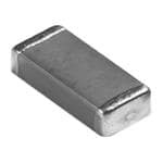
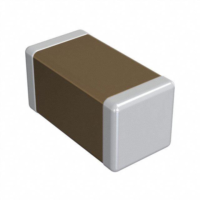
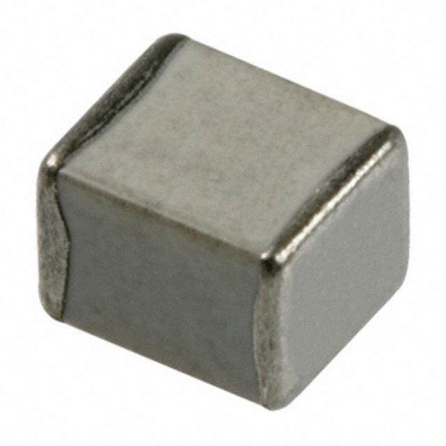
| 描述 | CAP CER 100PF 1KV 5% NPO 1206 |
| 产品分类 | |
| 品牌 | Yageo |
| 数据手册 | |
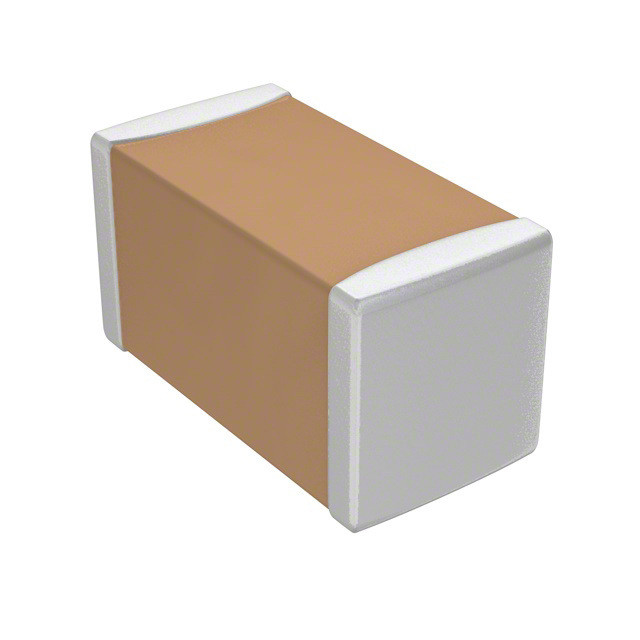
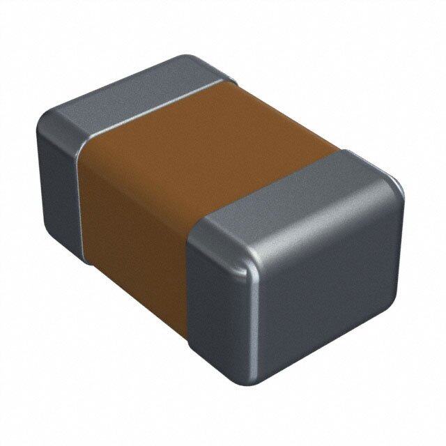
| 产品图片 |
|
| 产品型号 | CC1206JKNPOCBN101 |
| rohs | 无铅 / 符合限制有害物质指令(RoHS)规范要求 |
| 产品系列 | CC |
| 其它名称 | 311-1493-1 |
| 包装 | 剪切带 (CT) |
| 厚度(最大值) | 0.057"(1.45mm) |
| 大小/尺寸 | 0.126" 长 x 0.063" 宽(3.20mm x 1.60mm) |
| 安装类型 | 表面贴装,MLCC |
| 容差 | ±5% |
| 封装/外壳 | 1206(3216 公制) |
| 工作温度 | -55°C ~ 125°C |
| 应用 | 通用 |
| 引线形式 | - |
| 引线间距 | - |
| 标准包装 | 1 |
| 温度系数 | C0G,NP0 |
| 特性 | - |
| 电压-额定 | 1000V(1kV) |
| 电容 | 100pF |
| 等级 | - |
| 高度-安装(最大值) | - |


- 商务部:美国ITC正式对集成电路等产品启动337调查
- 曝三星4nm工艺存在良率问题 高通将骁龙8 Gen1或转产台积电
- 太阳诱电将投资9.5亿元在常州建新厂生产MLCC 预计2023年完工
- 英特尔发布欧洲新工厂建设计划 深化IDM 2.0 战略
- 台积电先进制程称霸业界 有大客户加持明年业绩稳了
- 达到5530亿美元!SIA预计今年全球半导体销售额将创下新高
- 英特尔拟将自动驾驶子公司Mobileye上市 估值或超500亿美元
- 三星加码芯片和SET,合并消费电子和移动部门,撤换高东真等 CEO
- 三星电子宣布重大人事变动 还合并消费电子和移动部门
- 海关总署:前11个月进口集成电路产品价值2.52万亿元 增长14.8%

PDF Datasheet 数据手册内容提取
DATA SHEET SURFACE-MOUNT CERAMIC MULTILAYER CAPACITORS High-Voltage NP0/X7R 1 KV TO 3 KV 10 pF to 33 nF RoHS compliant & Halogen Free 1 1 V. 8 1 0 2 3, 1 y ul J – n o ti a c cifi e p S t c u d o Pr
Product specification 2 S urface-Mount Ceramic Multilayer Capacitors High-Vo ltage NP0/ X7R 1 KV to 3 KV 13 SCOPE ORDERING INFORMATION - GLOBAL PART NUMBER, PHYCOMP This specification describes High- CTC & 12NC Voltage NP0/X7R series chip All part numbers are identified by the series, size, tolerance, TC material, capacitors wi th lead-free packing style, voltage, process code, termination and capacitance value. terminations. YYAAGGEEOO BBRRAANNDD oorrddeerriinngg ccooddee GLOBAL PART NUMBER (PREFERRED) APPLICATIONS PCs, Hard disk, Game PCs CC XXXX X X XXX X B X XXX (1) (2) (3) (4) (5) (6) (7) Power supplies LCD panel (1) SIZE – INCH BASED (METRIC) ADSL, Modem 0805 (2012) / 1206 (3216) / 1210 (3225) / 1808 (4520) / 1812 (4532) (2) TOLERANCE FEATURES C = ±0.25 pF Supplied in tape on reel D = ±0.5 pF Nickel-barrier end termination G = ±2% RoHS compliant J = ±5% Halogen Free compliant K = ±10% M = ±20% (3) PACKING STYLE R = Paper/PE taping reel; Reel 7 inch K = Blister taping reel; Reel 7 inch P = Paper/PE taping reel; Reel 13 inch F = Blister taping reel; Reel 13 inch C = Bulk case (4) TC MATERIAL NPO X7R (5) RATED VOLTAGE C = 1 KV D = 2 KV S = 2.5KV E = 3 KV (6) PROCESS N = NP0 B = Class 2 MLCC (7) CAPACITANCE VALUE 2 significant digits+number of zeros The 3rd digit signifies the multiplying factor, and letter R is decimal point Example: 121 = 12 x 101 = 120 pF www.yageo.com Jul. 13, 2018 V.11
Product specification 3 S urface-Mount Ceramic Multilayer Capacitors High-Vo ltage NP0/ X7R 1 KV to 3 KV 13 CONSTRUCTION The capacitor consists of a rectangular block of ceramic dielectric in w hich a number of interleaved m etal electrodes are contained. This structure gives rise to a high capacitance per unit volume. The inner electrodes are connected to the two end terminations and finally covered with a layer of plated tin (NiSn). The terminations are lead-free. A cross section of the structure is Fig. 1 Surface mounted multilayer cerami c capacitor construction shown in Fig.1. D IMENSION Table 1 For outlines see fig. 2 OOUUTTLLIINNEESS L / L (mm) L (mm) TY PE L1 (mm) W (mm) T (MM) m2in. 3 max. 4 min. F or dimension see Table 1 0805 2.0 ±0.20 1.25 ±0.20 0.25 0.75 0.70 1206 3.2 ±0.30 1.6 ±0.20 0.25 0.75 1.40 1210 3.2 ±0.30 2.5 ±0.20 Refer to 0.25 0.75 1.40 table 2 to 4 1808 4.5 ±0.40 2.0 ±0.30 0.25 0.75 2.20 1812 4.5 ±0.40 3.2 ±0.20 0.25 0.75 2.20 Fig. 2 cSeurrafamceic mcao puanctiteodr mdiumlteilnayseiorn www.yageo.com Jul. 13, 2018 V.11
Product specification 4 S urface-Mount Ceramic Multilayer Capacitors High-Vo ltage NP0/ X7R 1 KV to 3 KV 13 C APACITANCE RANGE & THICKNESS FOR NP0 Table 2 Sizes from 0805 to 1812 CA P. 08 05 1206 1210 1808 1812 1 KV 1 KV 2 KV 3 KV 1 KV 2 KV 1 KV 2 KV 3 KV 1 KV 2 KV 3 KV 10 pF 0.85± 0.1 1.25±0.2 1.25±0.2 1.25±0.2 1.6±0.2 1.25±0.2 1.25±0.2 1.25±0.2 12 pF 0.85±0.1 1.25±0.2 1.25±0.2 1.25±0.2 1.6±0.2 1.25±0.2 1.25±0.2 1.25±0.2 15 pF 0.85±0.1 1.25±0.2 1.25±0.2 1.25±0.2 1.6±0.2 1.25±0.2 1.25±0.2 1.25±0.2 18 pF 0.85±0.1 1.25±0.2 1.25±0.2 1.25±0.2 1.6±0.2 1.25±0.2 1.25±0.2 1.25±0.2 22 pF 0.85±0.1 1.25±0.2 1.25±0.2 1.25±0.2 1.6±0.2 1.25±0.2 1.25±0.2 1.25±0.2 27 pF 0.85±0.1 1.25±0.2 1.25±0.2 1.25±0.2 1.6±0.2 1.25±0.2 1.25±0.2 1.25±0.2 33 pF 0.85±0.1 1.25±0.2 1.25±0.2 1.25±0.2 1.25±0.2 1.25±0.2 1.25±0.2 1.25±0.2 1.6±0.2 1.25±0.2 1.25±0.2 1.25±0.2 39 pF 0.85±0.1 1.25±0.2 1.25±0.2 1.25±0.2 1.25±0.2 1.25±0.2 1.25±0.2 1.25±0.2 1.6±0.2 1.25±0.2 1.25±0.2 1.25±0.2 47 pF 0.85±0.1 1.25±0.2 1.25±0.2 1.25±0.2 1.25±0.2 1.25±0.2 1.25±0.2 1.25±0.2 1.6±0.2 1.25±0.2 1.25±0.2 1.25±0.2 56 pF 1.25±0.2 1.25±0.2 1.25±0.2 1.25±0.2 1.25±0.2 1.25±0.2 1.6±0.2 1.25±0.2 1.25±0.2 1.25±0.2 68 pF 1.25±0.2 1.25±0.2 1.25±0.2 1.25±0.2 1.25±0.2 1.25±0.2 1.6±0.2 1.25±0.2 1.25±0.2 1.25±0.2 82 pF 1.25±0.2 1.25±0.2 1.25±0.2 1.25±0.2 1.25±0.2 1.25±0.2 1.6±0.2 1.25±0.2 1.25±0.2 1.25±0.2 100 pF 1.25±0.2 1.25±0.2 1.25±0.2 1.25±0.2 1.25±0.2 1.25±0.2 1.6±0.2 1.25±0.2 1.25±0.2 1.25±0.2 120 pF 1.25±0.2 1.25±0.2 1.25±0.2 1.25±0.2 1.25±0.2 1.25±0.2 1.25±0.2 1.25±0.2 1.25±0.2 150 pF 1.25±0.2 1.25±0.2 1.25±0.2 1.25±0.2 1.25±0.2 1.25±0.2 1.25±0.2 1.25±0.2 1.25±0.2 180 pF 1.25±0.2 1.25±0.2 1.25±0.2 1.25±0.2 1.25±0.2 1.25±0.2 1.25±0.2 1.25±0.2 1.25±0.2 220 pF 1.25±0.2 1.25±0.2 1.25±0.2 1.25±0.2 1.25±0.2 1.25±0.2 1.25±0.2 1.25±0.2 1.25±0.2 270 pF 1.25±0.2 1.25±0.2 1.25±0.2 1.25±0.2 1.25±0.2 1.25±0.2 330 pF 1.25±0.2 1.25±0.2 1.25±0.2 1.25±0.2 1.25±0.2 1.25±0.2 390 pF 1.25±0.2 1.25±0.2 1.25±0.2 1.25±0.2 1.25±0.2 1.25±0.2 470 pF 1.25±0.2 1.25±0.2 1.25±0.2 1.25±0.2 1.25±0.2 1.25±0.2 560 pF 1.25±0.2 1.25±0.2 1.25±0.2 1.25±0.2 1.25±0.2 1.25±0.2 680 pF 1.25±0.2 1.25±0.2 1.25±0.2 1.25±0.2 1.25±0.2 820 pF 1.25±0.2 1.25±0.2 1.25±0.2 1.25±0.2 1.0 nF 1.25±0.2 1.25±0.2 1.25±0.2 1.25±0.2 1.2 nF 1.25±0.2 1.5 nF 1.25±0.2 1.8 nF 2.2 nF 2.7 nF 3.3 nF NOTE 1. Values in shaded cells indicate thickness class in mm 2. Capacitance value of non E-12 series is on request www.yageo.com Jul. 13, 2018 V.11
Product specification 5 S urface-Mount Ceramic Multilayer Capacitors High-Vo ltage NP0/ X7R 1 KV to 3 KV 13 C APACITANCE RANGE & THICKNESS FOR X7R Table 3 Sizes from 0805 to 1812 CA P. 08 05 1206 1210 1808 1812 1 KV 1 KV 2 KV 2.5KV 1 KV 2 KV 1 KV 2 KV 3 KV 1 KV 2 KV 3 KV 100 pF 150 pF 0.85±0.1 1.6±0.2 220 pF 0.85±0.1 1.25±0.2 1.25±0.2 1.25±0.2 1.25±0.2 1.6±0.2 330 pF 0.85±0.1 1.25±0.2 1.25±0.2 1.25±0.2 1.25±0.2 1.35±0.15 1.6±0.2 470 pF 0.85±0.1 1.25±0.2 1.25±0.2 1.25±0.2 1.25±0.2 1.35±0.15 1.35±0.15 1.6±0.2 680 pF 0.85±0.1 1.25±0.2 1.25±0.2 1.25±0.2 1.25±0.2 1.35±0.15 1.35±0.15 1.6±0.2 1.0 nF 0.85±0.1 1.25±0.2 1.25±0.2 1.6±0.2 1.25±0.2 1.25±0.2 1.35±0.15 1.35±0.15 2.0±0.2 1.35±0.15 1.35±0.15 1.6±0.2 1.5 nF 1.25±0.2 1.25±0.2 1.25±0.2 1.25±0.2 1.35±0.15 1.35±0.15 2.0±0.2 1.35±0.15 1.35±0.15 2.2 nF 1.25±0.2 1.25±0.2 1.60±0.2 1.35±0.15 1.6±0.2 1.35±0.15 1.35±0.15 3.3 nF 1.25±0.2 1.25±0.2 1.35±0.15 1.35±0.15 1.35±0.15 4.7 nF 1.25±0.2 1.25±0.2 1.35±0.15 1.35±0.15 1.35±0.15 6.8 nF 1.25±0.2 1.25±0.2 1.6±0.2 1.35±0.15 10 nF 1.25±0.2 1.25±0.2 1.6±0.2 1.35±0.15 15 nF 1.25±0.2 1.35±0.15 22 nF 1.6±0.2 1.35±0.15 33 nF 1.6±0.2 47 nF 68 nF 100 nF N OTE 1 . Values in shaded cells indicate thickness class in mm 2. Capacitance value of non E-6 series is on request 3 . For products with 5% tolerance, please contact local sales force before ordering www.yageo.com Jul. 13, 2018 V.11
Product specification 6 S urface-Mount Ceramic Multilayer Capacitors High-Vo ltage NP0/ X7R 1 KV to 3 KV 13 THICKNESS CLASSES AND PACKING QUANTITY Table 5 SIZ E THICKNESS TAPE WIDTH Ø180 MM / 7 INCH Ø 330 MM / 13 INCH QUANTITY Paper Blister Paper Blister CODE CLASSIFICATION QUANTITY PER REEL PER BULK CASE 0201 0.3 ±0.03 mm 8 mm 15,000 --- 50,000 --- --- 0402 0.5 ±0.05 mm 8 mm 10,000 --- 50,000 --- 50,000 0603 0.8 ±0.1 mm 8 mm 4,000 --- 15,000 --- 15,000 0.6 ±0.1 mm 8 mm 4,000 --- 20,000 --- 10,000 0.8 / 0.85 ±0.1 mm 8 mm 4,000 --- 15,000 --- 8,000 0805 1.00 ±0.1 mm 8 mm --- 3,000 --- 10,000 --- 1.25 ±0.2 mm 8 mm --- 3,000 --- 10,000 5,000 0.6 ±0.1 mm 8 mm 4,000 --- 20,000 --- --- 0.8 / 0.85 ±0.1 mm 8 mm 4,000 --- 15,000 --- --- 1.00 / 1.15 ±0.1 mm 8 mm --- 3,000 --- 10,000 --- 1206 1.25 ±0.2 mm 8 mm --- 3,000 --- 10,000 --- 1.6 ±0.15 mm 8 mm --- 2,500 --- 10,000 --- 1.6 ±0.2 mm 8 mm --- 2,000 --- 8,000 --- 0.6 / 0.7 ±0.1 mm 8 mm --- 4,000 --- 15,000 --- 0.85 ±0.1 mm 8 mm --- 4,000 --- 10,000 --- 1.15 ±0.1 mm 8 mm --- 3,000 --- 10,000 --- 1.15 ±0.15 mm 8 mm --- 3,000 --- 10,000 --- 1.25 ±0.2 mm 8 mm --- 3,000 --- --- --- 1210 1.5 ±0.1 mm 8 mm --- 2,000 --- --- --- 1.6 / 1.9 ±0.2 mm 8 mm --- 2,000 --- --- --- 2,000 2.0 ±0.2 mm 8 mm --- --- --- --- 1,000 1,000 2.5 ±0.2 mm 8 mm --- --- --- --- 500 1.15 ±0.15 mm 12 mm --- 3,000 --- --- --- 1.25 ±0.2 mm 12 mm --- 3,000 --- --- --- 1.35 ±0.15 mm 12 mm --- 2,000 --- --- --- 1808 1.5 ±0.1 mm 12 mm --- 2,000 --- --- --- 1.6 ±0.2 mm 12 mm --- 2,000 --- --- --- 2.0 ±0.2 mm 12 mm --- 2,000 --- --- --- 0.6 / 0.85 ±0.1 mm 12 mm --- 2,000 --- --- --- 1.15 ±0.1 mm 12 mm --- 1,000 --- --- --- 1.15 ±0.15 mm 12 mm --- 1,000 --- --- --- 1.25 ±0.2 mm 12 mm --- 1,000 --- --- --- 1812 1.35 ±0.15 mm 12 mm --- 1,000 --- --- --- 1.5 ±0.1 mm 12 mm --- 1,000 --- --- --- 1.6 ±0.2 mm 12 mm --- 1,000 --- --- --- 2.0 ±0.2 mm 12 mm --- 1,000 --- --- --- 2.5 ±0.2 mm 12 mm --- 500 --- --- --- www.yageo.com Jul. 13, 2018 V.11
Product specification 7 S urface-Mount Ceramic Multilayer Capacitors High-Vo ltage NP0/ X7R 1 KV to 3 KV 13 ELECTRICAL CHARACTERISTICS NNPP00//XX77RR DDIIEELLEECCTTRRIICC CCAAPPAACCIITTOORRSS;; NNIISSNN TTEERRMMIINNAATTIIOONNSS Unless other wise stated all electrical values apply at an ambient temperature of 20±1 °C, an atmospheric pressure of 8 6 to 106 kPa, and a relative humidity of 63 to 67%. Table 6 DESCRIPTION VALUE Capacitance range 10 pF to 33 nF Capacitance tolerance NP0 C < 10 pF ±0.25 pF, ±0.5 pF C ≥ 10 pF ±2%, ±5% X7R ±5% (1), ±10% Dissipation factor (D.F.) NP0 C < 30 pF ≤ 1 / ( 400 + 20C ) C ≥ 30 pF ≤ 0.1 % X7R ≤ 2.5 % Insulation resistance after 1 minute at Ur (DC) Rins ≥ 10 GΩ or Rins × C ≥ 500 seconds whichever is less Maximum capacitance change as a function of temperature (temperature characteristic/coefficient): NP0 ±30 ppm/°C X7R ±15% Operating temperature range: NP0/X7R –55 °C to +125 °C NOTE 1. ±5% tolerance of capacitance value isn't available for X7R full product range, please contact local sales force before ordering www.yageo.com Jul. 13, 2018 V.11
Product specification 8 S urface-Mount Ceramic Multilayer Capacitors High-Vo ltage NP0/ X7R 1 KV to 3 KV 13 HIGH-VOLTAGE NP0 Sample limits (b roken lines). Requirement levels (dotted lines) Fig. 3 Typical temperature coefficient as a function of Fig. 4 Typical tan δ as a function of temperature temperature HIGH-VOLTAGE X7R X Fig. 5 Typical capacitance change as a function of Fig. 6 Typical tan δ as a function of temperature temperature www.yageo.com Jul. 13, 2018 V.11
Product specification 9 S urface-Mount Ceramic Multilayer Capacitors High-Vo ltage NP0/ X7R 1 KV to 3 KV 13 SOLDERING RECOMMENDATION Table 7 SOLDERING SIZE MET HOD 0402 0603 0805 1206 ≥ 1210 Reflow Reflow only ≥ 1.0 µF ≥ 2.2 µF ≥ 4.7 µF Reflow only Reflow/Wave --- < 1.0 µF < 2.2 µF < 4.7 µF --- T ESTS AND REQUIREMENTS Table 8 Test procedures and requirements TEST TEST METHOD PROCEDURE REQUIREMENTS Mounting IEC 60384- 4.3 The capacitors may be mounted on printed-circuit boards or No visible damage 21/22 ceramic substrates Visual 4.4 Any applicable method using × 10 magnification In accordance with specification Inspection and Dimension Check Capacitance 4.5.1 Class 1: Within specified tolerance f = 1 MHz for C ≤ 1 nF, measuring at voltage 1 V at 20 °C rms f = 1 KHz for C > 1 nF, measuring at voltage 1 V at 20 °C rms Class 2: f = 1 KHz for C ≤ 10 µF, measuring at voltage 1 V at 20 °C rms Dissipation 4.5.2 Class 1: In accordance with specification Factor (D.F.) f = 1 MHz for C ≤ 1 nF , measuring at voltage 1 V at 20 °C rms f = 1 KHz for C > 1 nF, measuring at voltage 1 V at 20 °C rms Class 2: f = 1 KHz for C ≤ 10 µF, measuring at voltage 1 V at 20 °C rms Insulation 4.5.3 U ≤ 500 V: At Ur for 1 minute In accordance with specification r Resistance U > 500 V: At 500 V for 1 minute r www.yageo.com Jul. 13, 2018 V.11
Product specification 10 S urface-Mount Ceramic Multilayer Capacitors High-Vo ltage NP0/ X7R 1 KV to 3 KV 13 TEST TEST METHOD PROCEDURE REQUIREMENTS Temperature 4.6 Capacitance shall be measured by the steps shown <General purpose series> Coefficient in the following table. Class1: ∆ C/C: ±30ppm The capacitance change should be measured after 5 min at each specified temperature stage. Class2: X7R: ∆ C/C: ±15% Step Temperature(℃) Y5V: ∆ C/C: 22~-82% a 25±2 <High Capacitance series> b Lower temperature±3℃ Class2: c 25±2 X7R/X5R: ∆ C/C: ±15% Y5V: ∆ C/C: 22~-82% d Upper Temperature±2℃ e 25±2 (1) Class I Temperature Coefficient shall be calculated from the formula as below C2-C1 Temp, Coefficient = 106 [ppm/℃] C1 xΔT C1: Capacitance at step c C2: Capacitance at 125℃ ∆T: 100℃(=125℃-25℃) (2) Class II Capacitance Change shall be calculated from the formula as below C2-C1 ∆C = x 100% C1 C1: Capacitance at step c C2: Capacitance at step b or d Adhesion IEC 60384- 4.7 A force applied for 10 seconds to the line joining Force 21/22 the terminations and in a plane parallel to the size ≥ 0603: 5N substrate Bending 4.8 Mounting in accordance with IEC 60384-22 No visible damage Strength paragraph 4.3 Conditions: bending 1 mm at a rate of 1 mm/s, ∆C/C radius jig 5 mm Class 1: NP0: within ±1% or 0.5 pF, whichever is greater Class2: X7R: ±10% www.yageo.com Jul. 13, 2018 V.11
Product specification 11 S urface-Mount Ceramic Multilayer Capacitors High-Vo ltage NP0/ X7R 1 KV to 3 KV 13 TEST TEST METHOD PROCEDURE REQUIREMENTS Resistance to 4.9 Precondition: 150 +0/–10 °C for 1 hour, then Dissolution of the end face plating shall not Soldering keep for 24 ±1 hours at room temperature exceed 25% of the length of the edge Heat Preheating: for size ≤ 1206: 120 °C to 150 °C for concerned 1 minute ∆C/C Preheating: for size >1206: 100 °C to 120 °C for Class 1: 1 minute and 170 °C to 200 °C for 1 minute NP0: within ±0.5% or 0.5 pF, whichever is greater Solder bath temperature: 260 ±5 °C Class2: Dipping time: 10 ±0.5 seconds X7R: ±10% Recovery time: 24 ±2 hours D.F. within initial specified value R within initial specified value ins Solderability 4.10 Preheated to a temperature of 80 °C to 140 °C The solder should cover over 95% of the critical and maintained for 30 seconds to 60 seconds. area of each termination 1. Temperature: 235±5°C / Dipping time: 2 ±0.5 s 2. Temperature: 245±5°C / Dipping time: 3 ±0.5 s (lead free)Depth of immersion: 10mm Rapid Change IEC 60384- 4.11 Preconditioning; No visual damage of 21/22 150 +0/–10 °C for 1 hour, then keep for Temperature 24 ±1 hours at room temperature ∆C/C Class 1: 5 cycles with following detail: NP0: within ±1% or 1 pF, whichever is greater 30 minutes at lower category temperature Class2: 30 minutes at upper category temperature X7R: ±15% Recovery time 24 ±2 hours D.F. meet initial specified value R meet initial specified value ins Damp Heat 4.13 1. Preconditioning, class 2 only: No visual damage after recovery 150 +0/-10 °C /1 hour, then keep for ∆C/C 24 ±1 hour at room temp Class 1: 2. Initial measure: NP0: within ±2% or 1 pF, whichever is greater Spec: refer to initial spec C, D, IR Class2: 3. Damp heat test: 500 ±12 hours at 40 ±2 °C; X7R: ±15% 90 to 95% R.H. D.F. 4. Recovery: Class 1: Class 1: 6 to 24 hours NP0: ≤ 2 x specified value Class 2: 24 ±2 hours Class2: 5. Final measure: C, D, IR X7R: ≥ 25 V: ≤ 5% R ins P.S. If the capacitance value is less than the Class 1: minimum value permitted, then after the other NP0: ≥ 2,500 MΩ or R x C ≥ 25s whichever is ins r measurements have been made the capacitor shall less be preconditioned according to “IEC 60384 4.1” Class2: and then the requirement shall be met. X7R: ≥ 500 MΩ or R x C ≥ 25s whichever is ins r less www.yageo.com Jul. 13, 2018 V.11
Product specification 12 S urface-Mount Ceramic Multilayer Capacitors High-Vo ltage NP0/ X7R 1 KV to 3 KV 13 TEST TEST METHOD PROCEDURE REQUIREMENTS Endurance IEC 60384- 4.14 1. Preconditioning, class 2 only: No visual damage 21/22 150 +0/-10 °C /1 hour, then keep for 24 ±1 hour at room temp ∆C/C 2. Initial measure: Class1: Spec: refer to initial spec C, D, IR NP0: within ±2% or 1 pF, whichever is greater Class2: Endurance test: Temperature: NP0/X7R: 125 °C X7R: ±15% Specified stress voltage applied for 1,000 hours. D.F. High-Voltage series follows the stress conditions Class1: below: NP0: ≤ 2 x specified value Voltage NPO X7R Class2: X7R: ≥ 25 V: ≤ 5% ≤ 100V 2.0 x Ur 2.0 x Ur 200/250V 1.5 x Ur 1.5 x Ur Rins Class1: 500/630V 1.3 x Ur 1.2 x Ur NP0: ≥ 4,000 MΩ or ≥ 1KV 1.2 x Ur 1.1 x Ur R x C ≥ 40s whichever is less ins r 3. Recovery time: 24 ±2 hours Class2: 4. Final measure: C, D, IR X7R: ≥ 1,000 MΩ or Rins x Cr ≥ 50s whichever is less P.S. If the capacitance value is less than the minimum value permitted, then after the other measurements have been made the capacitor shall be preconditioned according to “IEC 60384 4.1” and then the requirement shall be met. Voltage Proof Specified stress voltage applied for 1~5 seconds No breakdown or flashover Ur ≤ 100 V: series applied 2.5 Ur 100 V < Ur ≤ 200 V series applied (1.5 Ur + 100) 200 V < Ur ≤ 500 V series applied (1.3 Ur + 100) Ur > 500 V: 1.3 Ur Ur ≥ 1KV: 1.2 Ur Charge/Discharge current less than 50mA www.yageo.com Jul. 13, 2018 V.11
Product specification 13 S urface-Mount Ceramic Multilayer Capacitors High-Vo ltage NP0/ X7R 1 KV to 3 KV 13 REVISION HISTORY REVISION DATE CHANGE NOTIFICATION DESCRIPTION Version 11 Jul . 13, 2018 - - Add NPO/1206/10pF to 47pF/3KV Version 10 Mar. 7, 2017 - - 0805 L4 spec updated Version 9 Jan. 16, 2017 - - Product range updated Version 8 Oct. 12, 2015 - - Product range updated Version 7 May 21, 2014 - - Product range updated Version 6 Jun. 17, 2012 - - Product range updated Version 5 Sep 25, 2012 - - Product range updated Version 4 Aug 08, 2011 - - Product range updated Version 3 Jan 19, 2011 - - Dimension updated - Add NP0 0805 1KV Version 2 Feb 02, 2010 - - Change to dual brand datasheet that describe High-Voltage NP0/X7R series with RoHS compliant - Replace the high voltage part of pdf files: UP-NP0X7R_HV_1K-to-4KV_1 and UY-NP0X7R_HV_1K-to-4KV_1 - Description of "Halogen Free compliant" added - Product range updated - Define global part number - Test method and procedure updated Version 1 Sep 30, 2005 - - Thickness revised Version 0 Sep 12, 2005 - - New www.yageo.com Jul. 13, 2018 V.11
Mouser Electronics Authorized Distributor Click to View Pricing, Inventory, Delivery & Lifecycle Information: Y ageo: CC1206KKX7RCBB102 CC1206JKNPODBN101 CC1808KKX7RDBB152 CC1812JKNPOEBN470 CC1812JKNPOEBN680 CC1812KKX7RDBB102 CC1812KKX7RCBB102 CC1812KKX7RDBB332 CC1812JKNPOCBN471 CC1812JKNPOCBN681 CC1812JKNPOCBN821 CC1812JKNPOEBN101 CC1812JKNPOEBN220 CC1812JKNPOEBN221 CC1812JKNPOEBN330 CC1808KKX7RDBB102 CC1812KKX7RCBB103 CC1812KKX7RDBB472 CC1206KKX7RDBB102 CC1812KKX7RCBB333 CC1812JKNPOEBN100 CC1808JKNPOEBN220 CC1206JKNPOCBN101 CC1206JKNPOCBN102 CC1206JKNPOCBN121 CC1206JKNPOCBN181 CC1206JKNPOCBN221 CC1206JKNPODBN470 CC1206KKX7RCBB472 CC1210JKNPOCBN471 CC1210KKX7RCBB102 CC1210KKX7RCBB103 CC1808JKNPOEBN100 CC1808JKNPOEBN101 CC1808JKNPOEBN270 CC1808JKNPOEBN330 CC1808JKNPOEBN680 CC1812JKNPOCBN101 CC1812JKNPOCBN102 CC1812JKNPOCBN151 CC1812JKNPOCBN152 CC1812JKNPOCBN221 CC1812JKNPOCBN331 CC1812JKNPODBN101 CC1812KKX7RCBB153 CC1812KKX7RCBB222 CC1812KKX7RCBB332 CC1812KKX7RCBB472 CC1812KKX7RDBB152 CC1812KKX7RDBB222 CC1206JRNPOCBN101 CC1206KKX7RCBB152 CC1206KKX7RCBB222 CC1808KKX7RDBB222 CC1206KKX7RCBB103 CC1206JKNPODBN330 CC1210KKX7RCBB223 CC1812KKX7RDBB103 CC1206JKNPOCBN151 CC1206JKNPOCBN220 CC1206JKNPOCBN330 CC1206JKNPOCBN331 CC1206JKNPOCBN470 CC1206JKNPOCBN471 CC1206JKNPOCBN560 CC1206JKNPOCBN680 CC1206JKNPOCBN681 CC1206JKNPOCBN821 CC1206JKNPODBN100 CC1206JKNPODBN121 CC1206JKNPODBN150 CC1206JKNPODBN181 CC1206JKNPODBN220 CC1206JKNPODBN221 CC1206JKNPODBN680 CC1206JKX7RDBB102 CC1206JRNPOCBN100 CC1206JRNPOCBN220 CC1206KKX7RCBB221 CC1206KKX7RCBB331 CC1206KKX7RCBB332 CC1206KKX7RCBB471 CC1206KKX7RCBB681 CC1206KKX7RCBB682 CC1206KKX7RDBB152 CC1206KKX7RDBB221 CC1206KKX7RDBB471 CC1206MKX7RDBB102 CC1210JKNPOCBN102 CC1210JKNPODBN101 CC1210JKNPODBN221 CC1210KKX7RCBB333 CC1210KKX7RCBB472 CC1210KKX7RDBB102 CC1210KKX7RDBB222 CC1808CKNPOEBN5R0 CC1808JKNPOCBN102 CC1808JKNPOCBN470 CC1808JKNPOCBN471 CC1808JKNPODBN221