ICGOO在线商城 > 集成电路(IC) > 逻辑 - 信号开关,多路复用器,解码器 > CBT3253APW,112
 Datasheet下载
- 型号: CBT3253APW,112
- 制造商: NXP Semiconductors
- 库位|库存: xxxx|xxxx
- 要求:
| 数量阶梯 | 香港交货 | 国内含税 |
| +xxxx | $xxxx | ¥xxxx |
查看当月历史价格
查看今年历史价格
CBT3253APW,112产品简介:
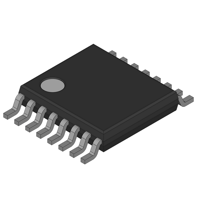
ICGOO电子元器件商城为您提供CBT3253APW,112由NXP Semiconductors设计生产,在icgoo商城现货销售,并且可以通过原厂、代理商等渠道进行代购。 CBT3253APW,112价格参考¥4.65-¥4.65。NXP SemiconductorsCBT3253APW,112封装/规格:逻辑 - 信号开关,多路复用器,解码器, 多路复用器/多路分解器 2 x 4:1 16-TSSOP。您可以下载CBT3253APW,112参考资料、Datasheet数据手册功能说明书,资料中有CBT3253APW,112 详细功能的应用电路图电压和使用方法及教程。
| 参数 | 数值 |
| 产品目录 | 集成电路 (IC)半导体 |
| 描述 | IC 1:4 FET MUX/DEMUX DL 16TSSOP编码器、解码器、复用器和解复用器 DUAL1OF4 FET |
| 产品分类 | |
| 品牌 | NXP Semiconductors |
| 产品手册 | |
| 产品图片 |
|
| rohs | 符合RoHS无铅 / 符合限制有害物质指令(RoHS)规范要求 |
| 产品系列 | 逻辑集成电路,编码器、解码器、复用器和解复用器,NXP Semiconductors CBT3253APW,11274CBT |
| 数据手册 | |
| 产品型号 | CBT3253APW,112 |
| 产品 | Multiplexers |
| 产品培训模块 | http://www.digikey.cn/PTM/IndividualPTM.page?site=cn&lang=zhs&ptm=24983 |
| 产品种类 | 编码器、解码器、复用器和解复用器 |
| 传播延迟时间 | 0.25 ns |
| 供应商器件封装 | 16-TSSOP |
| 其它名称 | 568-3629-5 |
| 包装 | 管件 |
| 商标 | NXP Semiconductors |
| 安装类型 | 表面贴装 |
| 安装风格 | SMD/SMT |
| 封装 | Tube |
| 封装/外壳 | 16-TSSOP(0.173",4.40mm 宽) |
| 封装/箱体 | TSSOP-16 |
| 工作温度 | -40°C ~ 85°C |
| 工厂包装数量 | 2400 |
| 最大工作温度 | + 85 C |
| 最小工作温度 | - 40 C |
| 标准包装 | 96 |
| 独立电路 | 1 |
| 电压-电源 | 4.5 V ~ 5.5 V |
| 电压源 | 单电源 |
| 电流-输出高,低 | - |
| 电源电压-最大 | 5.5 V |
| 电源电压-最小 | 4.5 V |
| 电路 | 2 x 4:1 |
| 类型 | FET 多路复用器/多路分解器 |
| 输入/输出线数量 | 8 / 2 |
| 输入线路数量 | 8 |
| 输出线路数量 | 2 |
| 逻辑系列 | CBT |
| 零件号别名 | CBT3253APW |


- 商务部:美国ITC正式对集成电路等产品启动337调查
- 曝三星4nm工艺存在良率问题 高通将骁龙8 Gen1或转产台积电
- 太阳诱电将投资9.5亿元在常州建新厂生产MLCC 预计2023年完工
- 英特尔发布欧洲新工厂建设计划 深化IDM 2.0 战略
- 台积电先进制程称霸业界 有大客户加持明年业绩稳了
- 达到5530亿美元!SIA预计今年全球半导体销售额将创下新高
- 英特尔拟将自动驾驶子公司Mobileye上市 估值或超500亿美元
- 三星加码芯片和SET,合并消费电子和移动部门,撤换高东真等 CEO
- 三星电子宣布重大人事变动 还合并消费电子和移动部门
- 海关总署:前11个月进口集成电路产品价值2.52万亿元 增长14.8%


PDF Datasheet 数据手册内容提取
CBT3253A Dual 1-of-4 FET multiplexer/demultiplexer Rev. 5 — 9 May 2017 Product data sheet 1 General description The CBT3253A is a dual 1-of-4 high-speed TTL-compatible FET multiplexer/ demultiplexer. The low ON-resistance of the switch allows inputs to be connected to outputs without adding propagation delay or generating additional ground bounce noise. When the output enable input (nOE) is LOW, the 1-of-4 multiplexer/demultiplexer is enabled. The data path is selected by the select control inputs (S0, S1). When nOE is HIGH, the 1-of-4 multiplexer/demultiplexer is disabled. The switch terminals are in the high impedance OFF-state, independent of S0 and S1. The CBT3253A is characterized for operation from -40 °C to +85 °C. 2 Features and benefits • 5 Ω switch connection between two ports • TTL-compatible input levels • Minimal propagation delay through the switch • Latch-up protection exceeds 100 mA per JEDEC standard JESD78 class II level A • ESD protection: –HBM JESD22-A114E exceeds 2000 V –MM JESD22-A115-A exceeds 200 V –CDM JESD22-C101C exceeds 1000 V • Multiple package options • Specified from -40 °C to +85 °C 3 Ordering information Table 1. Ordering information Type number Temperature range Package Name Description Version CBT3253AD -40 °C to +85 °C SO16 plastic small outline package; 16 leads; SOT109-1 body width 3.9 mm CBT3253ADB -40 °C to +85 °C SSOP16 plastic shrink small outline package; 16 leads; SOT338-1 body width 5.3 mm [1] CBT3253ADS -40 °C to +85 °C SSOP16 plastic shrink small outline package; 16 leads; SOT519-1 body width 3.9 mm; lead pitch 0.635 mm CBT3253APW -40 °C to +85 °C TSSOP16 plastic thin shrink small outline package; 16 leads; SOT403-1 body width 4.4 mm [1] Also known as QSOP16.
Nexperia CBT3253A Dual 1-of-4 FET multiplexer/demultiplexer 4 Functional diagram 7 6 1A 1B1 5 1B2 4 1B3 3 1B4 9 10 2A 2B1 11 2B2 12 2B3 13 2B4 14 S0 2 S1 1 1OE 15 2OE aaa-015421 Figure 1. Logic diagram CBT3253A All information provided in this document is subject to legal disclaimers. © Nexperia B.V. 2017. All rights reserved. Product data sheet Rev. 5 — 9 May 2017 2 / 15
Nexperia CBT3253A Dual 1-of-4 FET multiplexer/demultiplexer 5 Pinning information 5.1 Pinning CBT3253A 1OE 1 16 VCC S1 2 15 2OE CBT3253A 1B4 3 14 S0 1OE 1 16 VCC 1B3 4 13 2B4 S1 2 15 2OE 1B4 3 14 S0 1B2 5 12 2B3 1B3 4 13 2B4 1B1 6 11 2B2 1B2 5 12 2B3 1B1 6 11 2B2 1A 7 10 2B1 1A 7 10 2B1 GND 8 9 2A GND 8 9 2A 002aab824 002aab827 Figure 2. Pin configuration SOT109-1 (SO16) and Figure 3. Pin configuration SOT338-1 (SSOP16) and SOT519-1 (SSOP16) SOT403-1 (TSSOP16) 5.2 Pin description Table 2. Pin description Symbol Pin Description 1OE, 2OE 1, 15 output enable (active LOW) S1, S0 2, 14 select control input 1B4, 1B3, 1B2, 1B1 3, 4, 5, 6 1B outputs/inputs 1A 7 1A input/output GND 8 ground (0 V) 2A 9 2A input/output 2B1, 2B2, 2B3, 2B4 10, 11, 12, 13 2B outputs/inputs V 16 positive supply voltage CC CBT3253A All information provided in this document is subject to legal disclaimers. © Nexperia B.V. 2017. All rights reserved. Product data sheet Rev. 5 — 9 May 2017 3 / 15
Nexperia CBT3253A Dual 1-of-4 FET multiplexer/demultiplexer 6 Functional description [1] Table 3. Function selection Inputs Switch 1OE 2OE S1 S0 X H X X disconnect 2A to 2Bn H X X X disconnect 1A to 1Bn L L L L 1A to 1B1 and 2A to 2B1 L L L H 1A to 1B2 and 2A to 2B2 L L H L 1A to 1B3 and 2A to 2B3 L L H H 1A to 1B4 and 2A to 2B4 [1] H = HIGH voltage level; L = LOW voltage level; X = Don’t care. 7 Limiting values Table 4. Limiting values In accordance with the Absolute Maximum Rating System (IEC 60134). Voltages are referenced to GND (ground = 0 V). Symbol Parameter Conditions Min Max Unit V supply voltage -0.5 +7.0 V CC [1] V input voltage -0.5 +7.0 V I I switch current continuous current through each switch - 128 mA SW I input clamping current V < 0 V -50 - mA IK I T storage temperature -65 +150 °C stg P total power dissipation T = -40 °C to +85 °C tot amb [2] SO16 package - 500 mW [3] SSOP16 package - 500 mW [3] TSSOP16 package - 500 mW [1] The input and output negative voltage ratings may be exceeded if the input and output clamp current ratings are observed. [2] For SO16 package: Ptot derates linearly with 8 mW/K above 70 °C. [3] For SSOP16 and TSSOP16 package: Ptot derates linearly with 5.5 mW/K above 70 °C. 8 Recommended operating conditions Table 5. Operating conditions All unused control inputs of the device must be held at V or GND to ensure proper device operation. CC Symbol Parameter Conditions Min Max Unit V supply voltage 4.5 5.5 V CC V HIGH-level input voltage 2.0 - V IH V LOW-level input voltage - 0.8 V IL T ambient temperature operating in free-air -40 +85 °C amb CBT3253A All information provided in this document is subject to legal disclaimers. © Nexperia B.V. 2017. All rights reserved. Product data sheet Rev. 5 — 9 May 2017 4 / 15
Nexperia CBT3253A Dual 1-of-4 FET multiplexer/demultiplexer 9 Static characteristics Table 6. Static characteristics At recommended operating conditions. Voltages are referenced to GND (ground = 0 V). T = -40 °C to +85 °C. amb [1] Symbol Parameter Conditions Min Typ Max Unit V input clamping voltage V = 4.5 V; I = -18 mA - - -1.2 V IK CC I V pass voltage V = V = 5.0 V; I = -100 μA 3.6 3.9 4.2 V pass I CC O I input leakage current V = 5.5 V; V = GND or 5.5 V - - ±1 μA I CC I I supply current V = 5.5 V; I = 0 mA;V = V or GND - - 3 μA CC CC O I CC [2] ΔI additional supply current per input; V = 5.5 V; one input at 3.4 V, - - 2.5 mA CC CC other inputs at V or GND CC C input capacitance control pins; V = 3 V or 0 V - 4.5 - pF I I C off-state input/output A port; V = 3 V or 0 V; nOE = V - 11.4 - pF io(off) O CC capacitance B port; V = 3 V or 0 V; nOE = V - 3.8 - pF O CC C on-state input/output A port and B port - 18.6 - pF io(on) capacitance [3] R ON resistance V = 4.5 V ON CC V = 0 V; I = 64 mA - 5 7 Ω I I V = 0 V; I = 30 mA - 5 7 Ω I I V = 2.4 V; I = -15 mA - 10 15 Ω I I [1] All typical values are measured at VCC = 5 V; Tamb = 25 °C. [2] This is the increase in supply current for each input that is at the specified TTL voltage level rather than VCC or GND. [3] Measured by the voltage drop between the A and the B terminals at the indicated current through the switch. The lowest voltage of the two (A or B) terminals determines the ON resistance. 10 Dynamic characteristics Table 7. Dynamic characteristics T = -40 °C to +85 °C; V = 4.5 V to 5.5 V; for test circuit, see Figure 6. amb CC Symbol Parameter Conditions Min Max Unit [1][2] t propagation delay Sn to nA; see Figure 4 1.2 6.2 ns pd [1][2] nA to nBn or nBn to nA; see Figure 4 - 0.25 ns [3] t enable time Sn to nBn; see Figure 5 1.3 6.3 ns en [3] nOE to nA or nBn; see Figure 5 1.4 6.4 ns [4] t disable time Sn to nBn; see Figure 5 1.1 7.2 ns dis [4] nOE to nA or nBn; see Figure 5 1.0 7 ns [1] This parameter is warranted but not production tested. The propagation delay is based on the RC time constant of the typical ON resistance of the switch and a load capacitance, when driven by an ideal voltage source (zero output impedance). [2] tPLH and tPHL are the same as tpd. [3] tPZL and tPZH are the same as ten. [4] tPLZ and tPHZ are the same as tdis. CBT3253A All information provided in this document is subject to legal disclaimers. © Nexperia B.V. 2017. All rights reserved. Product data sheet Rev. 5 — 9 May 2017 5 / 15
Nexperia CBT3253A Dual 1-of-4 FET multiplexer/demultiplexer 10.1 Waveforms and test circuit VI input VM VM 0V tPHL tPLH VOH output VM VM VOL 001aai367 Measurement points are given in Table 8. V and V are typical voltage output levels that occur with the output load. OL OH Figure 4. The input (nA; nBn) to output (nBn; nA) or input (Sn) to output (nA) propagation delay times VI nOE,Sninput VM VM GND tPLZ tPZL VCC output LOW-to-OFF VM OFF-to-LOW VOL VX tPHZ tPZH VOH VY output HIGH-to-OFF VM OFF-to-HIGH GND switch switch switch enabled disabled enabled 001aal212 Measurement points are given in Table 8. V and V are typical voltage output levels that occur with the output load. OL OH Figure 5. Enable and disable times Table 8. Measurement points Supply voltage Input Output V V V V V V CC I M M X Y 4.5 V to 5.5 V GND to 3.0 V 1.5 V 1.5 V V + 0.3 V V - 0.3 V OL OH CBT3253A All information provided in this document is subject to legal disclaimers. © Nexperia B.V. 2017. All rights reserved. Product data sheet Rev. 5 — 9 May 2017 6 / 15
Nexperia CBT3253A Dual 1-of-4 FET multiplexer/demultiplexer tW VI 90% negative pulse VM VM 10% 0V tf tr tr tf VI 90% positive pulse VM VM 10% 0V tW VEXT VCC RL VI VO G DUT RT CL RL 001aae331 Test data is given in Table 9. Definitions for test circuit: R = Load resistance. L C = Load capacitance including jig and probe capacitance. L R = Termination resistance should be equal to the output impedance Z of the pulse generator. T o V = External voltage for measuring switching times. EXT Figure 6. Test circuit for measuring switching times Table 9. Test data Supply voltage Input Load V EXT V V t, t C R t , t t , t t , t CC I r f L L PLH PHL PLZ PZL PHZ PZH 4.5 V to 5.5 V GND to 3.0 V ≤ 2.5 ns 50 pF 500 Ω open 7.0 V open CBT3253A All information provided in this document is subject to legal disclaimers. © Nexperia B.V. 2017. All rights reserved. Product data sheet Rev. 5 — 9 May 2017 7 / 15
Nexperia CBT3253A Dual 1-of-4 FET multiplexer/demultiplexer 11 Package outline SO16:plasticsmalloutlinepackage;16leads;bodywidth3.9mm SOT109-1 D E A X c y HE v M A Z 16 9 Q A2 A1 (A3) A pin1index θ Lp 1 8 L e w M detailX bp 0 2.5 5mm scale DIMENSIONS(inchdimensionsarederivedfromtheoriginalmmdimensions) UNIT mAax. A1 A2 A3 bp c D(1) E(1) e HE L Lp Q v w y Z(1) θ 0.25 1.45 0.49 0.25 10.0 4.0 6.2 1.0 0.7 0.7 mm 1.75 0.25 1.27 1.05 0.25 0.25 0.1 0.10 1.25 0.36 0.19 9.8 3.8 5.8 0.4 0.6 0.3 8o 0.010 0.057 0.019 0.0100 0.39 0.16 0.244 0.039 0.028 0.028 0o inches 0.069 0.01 0.05 0.041 0.01 0.01 0.004 0.004 0.049 0.014 0.0075 0.38 0.15 0.228 0.016 0.020 0.012 Note 1.Plasticormetalprotrusionsof0.15mm(0.006inch)maximumpersidearenotincluded. OUTLINE REFERENCES EUROPEAN ISSUEDATE VERSION IEC JEDEC JEITA PROJECTION 99-12-27 SOT109-1 076E07 MS-012 03-02-19 Figure 7. Package outline SOT109-1 (SO16) CBT3253A All information provided in this document is subject to legal disclaimers. © Nexperia B.V. 2017. All rights reserved. Product data sheet Rev. 5 — 9 May 2017 8 / 15
Nexperia CBT3253A Dual 1-of-4 FET multiplexer/demultiplexer SSOP16:plasticshrinksmalloutlinepackage;16leads;bodywidth5.3mm SOT338-1 D E A X c y HE v M A Z 16 9 Q A2 A1 (A3) A pin1index θ Lp L 1 8 detailX w M e bp 0 2.5 5mm scale DIMENSIONS(mmaretheoriginaldimensions) UNIT mAax. A1 A2 A3 bp c D(1) E(1) e HE L Lp Q v w y Z(1) θ 0.21 1.80 0.38 0.20 6.4 5.4 7.9 1.03 0.9 1.00 8o mm 2 0.05 1.65 0.25 0.25 0.09 6.0 5.2 0.65 7.6 1.25 0.63 0.7 0.2 0.13 0.1 0.55 0o Note 1.Plasticormetalprotrusionsof0.25mmmaximumpersidearenotincluded. OUTLINE REFERENCES EUROPEAN ISSUEDATE VERSION IEC JEDEC JEITA PROJECTION 99-12-27 SOT338-1 MO-150 03-02-19 Figure 8. Package outline SOT338-1 (SSOP16) CBT3253A All information provided in this document is subject to legal disclaimers. © Nexperia B.V. 2017. All rights reserved. Product data sheet Rev. 5 — 9 May 2017 9 / 15
Nexperia CBT3253A Dual 1-of-4 FET multiplexer/demultiplexer SSOP16:plasticshrinksmalloutlinepackage;16leads;bodywidth3.9mm;leadpitch0.635mm SOT519-1 D E A X c y HE v M A Z 16 9 A2 A A1 (A3) θ Lp L 1 8 detailX e w M bp 0 2.5 5mm scale DIMENSIONS(mmaretheoriginaldimensions) UNIT mAax. A1 A2 A3 bp c D(1) E(1) e HE L Lp v w y Z(1) θ mm 1.73 00..2150 11..5450 0.25 00..3210 00..2158 54..08 43..08 0.635 65..28 1 00..8491 0.2 0.18 0.09 00..1085 80oo Note 1.Plasticormetalprotrusionsof0.2mmmaximumpersidearenotincluded. OUTLINE REFERENCES EUROPEAN ISSUEDATE VERSION IEC JEDEC JEITA PROJECTION 99-05-04 SOT519-1 03-02-18 Figure 9. Package outline SOT519-1 (SSOP16) CBT3253A All information provided in this document is subject to legal disclaimers. © Nexperia B.V. 2017. All rights reserved. Product data sheet Rev. 5 — 9 May 2017 10 / 15
Nexperia CBT3253A Dual 1-of-4 FET multiplexer/demultiplexer TSSOP16:plasticthinshrinksmalloutlinepackage;16leads;bodywidth4.4mm SOT403-1 D E A X c y HE v M A Z 16 9 Q A2 (A3) A pin1index A1 θ Lp L 1 8 detailX w M e bp 0 2.5 5mm scale DIMENSIONS(mmaretheoriginaldimensions) UNIT mAax. A1 A2 A3 bp c D(1) E(2) e HE L Lp Q v w y Z(1) θ 0.15 0.95 0.30 0.2 5.1 4.5 6.6 0.75 0.4 0.40 8o mm 1.1 0.05 0.80 0.25 0.19 0.1 4.9 4.3 0.65 6.2 1 0.50 0.3 0.2 0.13 0.1 0.06 0o Notes 1.Plasticormetalprotrusionsof0.15mmmaximumpersidearenotincluded. 2.Plasticinterleadprotrusionsof0.25mmmaximumpersidearenotincluded. OUTLINE REFERENCES EUROPEAN ISSUEDATE VERSION IEC JEDEC JEITA PROJECTION 99-12-27 SOT403-1 MO-153 03-02-18 Figure 10. Package outline SOT403-1 (TSSOP16) CBT3253A All information provided in this document is subject to legal disclaimers. © Nexperia B.V. 2017. All rights reserved. Product data sheet Rev. 5 — 9 May 2017 11 / 15
Nexperia CBT3253A Dual 1-of-4 FET multiplexer/demultiplexer 12 Abbreviations Table 10. Abbreviations Acronym Description CDM Charged Device Model DUT Device Under Test ESD ElectroStatic Discharge HBM Human Body Model MM Machine Model TTL Transistor-Transistor Logic 13 Revision history Table 11. Revision history Document ID Release date Data sheet status Change notice Supersedes CBT3253A v.5 20170509 Product data sheet - CBT3253A v.4 Modifications: • The format of this data sheet has been redesigned to comply with the identity guidelines of Nexperia. • Legal texts have been adapted to the new company name where appropriate. CBT3253A v.4 20141031 Product data sheet - CBT3253A v.3 Modifications: • Section 1: text changed to align with the function of the device. • Figure 1: schematic changed.. • Section 6: switch description changed to align with the function of the device. • Table 7: typo corrected, the conditions for enable and disable times are swapped. CBT3253A v.3 20130924 Product data sheet - CBT3253A v.2 Modifications: Section 9 values for pass voltage modified. CBT3253A v.2 20070208 Product data sheet - CBT3253A v.1 CBT3253A v.1 20051024 Product data sheet - - CBT3253A All information provided in this document is subject to legal disclaimers. © Nexperia B.V. 2017. All rights reserved. Product data sheet Rev. 5 — 9 May 2017 12 / 15
Nexperia CBT3253A Dual 1-of-4 FET multiplexer/demultiplexer 14 Legal information 14.1 Data sheet status Document status[1][2] Product status[3] Definition Objective [short] data sheet Development This document contains data from the objective specification for product development. Preliminary [short] data sheet Qualification This document contains data from the preliminary specification. Product [short] data sheet Production This document contains the product specification. [1] Please consult the most recently issued document before initiating or completing a design. [2] The term 'short data sheet' is explained in section "Definitions". [3] The product status of device(s) described in this document may have changed since this document was published and may differ in case of multiple devices. The latest product status information is available on the Internet at URL http://www.nexperia.com. systems or equipment, nor in applications where failure or malfunction of an Nexperia product can reasonably be expected to result in personal 14.2 Definitions injury, death or severe property or environmental damage. Nexperia and its suppliers accept no liability for inclusion and/or use of Nexperia products in Draft — The document is a draft version only. The content is still under such equipment or applications and therefore such inclusion and/or use is at internal review and subject to formal approval, which may result in the customer’s own risk. modifications or additions. Nexperia does not give any representations or warranties as to the accuracy or completeness of information included herein Applications — Applications that are described herein for any of these and shall have no liability for the consequences of use of such information. products are for illustrative purposes only. Nexperia makes no representation or warranty that such applications will be suitable for the specified use Short data sheet — A short data sheet is an extract from a full data sheet without further testing or modification. Customers are responsible for the with the same product type number(s) and title. A short data sheet is design and operation of their applications and products using Nexperia intended for quick reference only and should not be relied upon to contain products, and Nexperia accepts no liability for any assistance with detailed and full information. For detailed and full information see the applications or customer product design. It is customer’s sole responsibility relevant full data sheet, which is available on request via the local Nexperia to determine whether the Nexperia product is suitable and fit for the sales office. In case of any inconsistency or conflict with the short data sheet, customer’s applications and products planned, as well as for the planned the full data sheet shall prevail. application and use of customer’s third party customer(s). Customers should provide appropriate design and operating safeguards to minimize the risks Product specification — The information and data provided in a Product associated with their applications and products. Nexperia does not accept data sheet shall define the specification of the product as agreed between any liability related to any default, damage, costs or problem which is based Nexperia and its customer, unless Nexperia and customer have explicitly on any weakness or default in the customer’s applications or products, or agreed otherwise in writing. In no event however, shall an agreement be the application or use by customer’s third party customer(s). Customer is valid in which the Nexperia product is deemed to offer functions and qualities responsible for doing all necessary testing for the customer’s applications beyond those described in the Product data sheet. and products using Nexperia products in order to avoid a default of the applications and the products or of the application or use by customer’s third party customer(s). Nexperia does not accept any liability in this respect. 14.3 Disclaimers Limiting values — Stress above one or more limiting values (as defined in the Absolute Maximum Ratings System of IEC 60134) will cause permanent Limited warranty and liability — Information in this document is believed damage to the device. Limiting values are stress ratings only and (proper) to be accurate and reliable. However, Nexperia does not give any operation of the device at these or any other conditions above those representations or warranties, expressed or implied, as to the accuracy given in the Recommended operating conditions section (if present) or the or completeness of such information and shall have no liability for the Characteristics sections of this document is not warranted. Constant or consequences of use of such information. Nexperia takes no responsibility repeated exposure to limiting values will permanently and irreversibly affect for the content in this document if provided by an information source outside the quality and reliability of the device. of Nexperia. In no event shall Nexperia be liable for any indirect, incidental, punitive, special or consequential damages (including - without limitation - lost profits, lost savings, business interruption, costs related to the removal Terms and conditions of commercial sale — Nexperia products are or replacement of any products or rework charges) whether or not such sold subject to the general terms and conditions of commercial sale, as damages are based on tort (including negligence), warranty, breach of published at http://www.nexperia.com/profile/terms, unless otherwise agreed contract or any other legal theory. Notwithstanding any damages that in a valid written individual agreement. In case an individual agreement is customer might incur for any reason whatsoever, Nexperia's aggregate and concluded only the terms and conditions of the respective agreement shall cumulative liability towards customer for the products described herein shall apply. Nexperia hereby expressly objects to applying the customer’s general be limited in accordance with the Terms and conditions of commercial sale of terms and conditions with regard to the purchase of Nexperia products by Nexperia. customer. Right to make changes — Nexperia reserves the right to make changes No offer to sell or license — Nothing in this document may be interpreted to information published in this document, including without limitation or construed as an offer to sell products that is open for acceptance or specifications and product descriptions, at any time and without notice. This the grant, conveyance or implication of any license under any copyrights, document supersedes and replaces all information supplied prior to the patents or other industrial or intellectual property rights. publication hereof. Export control — This document as well as the item(s) described herein Suitability for use — Nexperia products are not designed, authorized or may be subject to export control regulations. Export might require a prior warranted to be suitable for use in life support, life-critical or safety-critical authorization from competent authorities. CBT3253A All information provided in this document is subject to legal disclaimers. © Nexperia B.V. 2017. All rights reserved. Product data sheet Rev. 5 — 9 May 2017 13 / 15
Nexperia CBT3253A Dual 1-of-4 FET multiplexer/demultiplexer Non-automotive qualified products — Unless this data sheet expressly design and use of the product for automotive applications beyond Nexperia's states that this specific Nexperia product is automotive qualified, the standard warranty and Nexperia's product specifications. product is not suitable for automotive use. It is neither qualified nor tested in accordance with automotive testing or application requirements. Nexperia Translations — A non-English (translated) version of a document is for accepts no liability for inclusion and/or use of non-automotive qualified reference only. The English version shall prevail in case of any discrepancy products in automotive equipment or applications. In the event that customer between the translated and English versions. uses the product for design-in and use in automotive applications to automotive specifications and standards, customer (a) shall use the product without Nexperia's warranty of the product for such automotive applications, use and specifications, and (b) whenever customer uses the product for 14.4 Trademarks automotive applications beyond Nexperia's specifications such use shall be solely at customer’s own risk, and (c) customer fully indemnifies Nexperia Notice: All referenced brands, product names, service names and for any liability, damages or failed product claims resulting from customer trademarks are the property of their respective owners. CBT3253A All information provided in this document is subject to legal disclaimers. © Nexperia B.V. 2017. All rights reserved. Product data sheet Rev. 5 — 9 May 2017 14 / 15
Nexperia CBT3253A Dual 1-of-4 FET multiplexer/demultiplexer Contents 1 General description ............................................1 2 Features and benefits .........................................1 3 Ordering information ..........................................1 4 Functional diagram .............................................2 5 Pinning information ............................................3 5.1 Pinning ...............................................................3 5.2 Pin description ...................................................3 6 Functional description ........................................4 7 Limiting values ....................................................4 8 Recommended operating conditions ................4 9 Static characteristics ..........................................5 10 Dynamic characteristics .....................................5 10.1 Waveforms and test circuit ................................6 11 Package outline ...................................................8 12 Abbreviations ....................................................12 13 Revision history ................................................12 14 Legal information ..............................................13 Please be aware that important notices concerning this document and the product(s) described herein, have been included in section 'Legal information'. © Nexperia B.V. 2017. All rights reserved. For more information, please visit: http://www.nexperia.com For sales office addresses, please send an email to: salesaddresses@nexperia.com Date of release: 9 May 2017 Document identifier: CBT3253A