ICGOO在线商城 > 集成电路(IC) > PMIC - 监控器 > CAT811TTBI-T3

 Datasheet下载
- 型号: CAT811TTBI-T3
- 制造商: ON Semiconductor
- 库位|库存: xxxx|xxxx
- 要求:
| 数量阶梯 | 香港交货 | 国内含税 |
| +xxxx | $xxxx | ¥xxxx |
查看当月历史价格
查看今年历史价格
CAT811TTBI-T3产品简介:
ICGOO电子元器件商城为您提供CAT811TTBI-T3由ON Semiconductor设计生产,在icgoo商城现货销售,并且可以通过原厂、代理商等渠道进行代购。 CAT811TTBI-T3价格参考。ON SemiconductorCAT811TTBI-T3封装/规格:PMIC - 监控器, Supervisor Push-Pull, Totem Pole 1 Channel SOT-143。您可以下载CAT811TTBI-T3参考资料、Datasheet数据手册功能说明书,资料中有CAT811TTBI-T3 详细功能的应用电路图电压和使用方法及教程。
| 参数 | 数值 |
| 产品目录 | 集成电路 (IC)半导体 |
| 描述 | IC SUPERVISOR PP ACT LO SOT143-4监控电路 3.08V Push-Pull Low |
| 产品分类 | |
| 品牌 | ON Semiconductor |
| 产品手册 | |
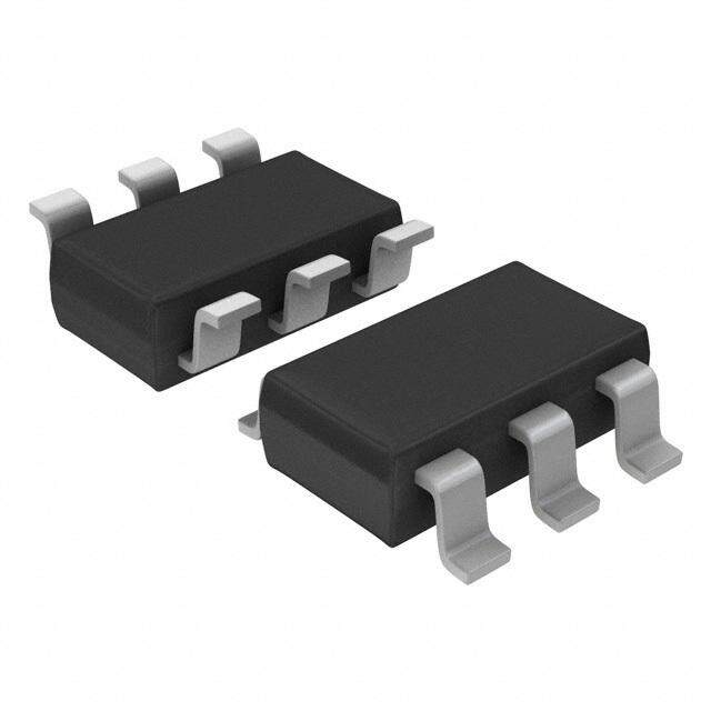
| 产品图片 |
|
| rohs | 符合RoHS无铅 / 符合限制有害物质指令(RoHS)规范要求 |
| 产品系列 | 电源管理 IC,监控电路,ON Semiconductor CAT811TTBI-T3- |
| NumberofInputsMonitored | 1 Input |
| 数据手册 | |
| 产品型号 | CAT811TTBI-T3 |
| 产品目录页面 | |
| 产品种类 | 监控电路 |
| 人工复位 | Manual Reset |
| 供应商器件封装 | SOT-143 |
| 其它名称 | CAT811TTBI-T3DKR |
| 功率失效检测 | No |
| 包装 | Digi-Reel® |
| 受监控电压数 | 1 |
| 商标 | ON Semiconductor |
| 复位 | 低有效 |
| 复位超时 | 最小为 140 ms |
| 安装类型 | 表面贴装 |
| 安装风格 | SMD/SMT |
| 封装 | Reel |
| 封装/外壳 | TO-253-4,TO-253AA |
| 封装/箱体 | SOT-143-4 |
| 工作温度 | -40°C ~ 85°C |
| 工作电源电流 | 8 uA |
| 工厂包装数量 | 3000 |
| 最大功率耗散 | 320 mW |
| 最大工作温度 | + 85 C |
| 最小工作温度 | - 40 C |
| 标准包装 | 1 |
| 欠电压阈值 | 3.08 V |
| 电压-阈值 | 3.08V |
| 电池备用开关 | No Backup |
| 电源电压-最大 | 5 V, 3.3 V, 3 V, 2.5 V |
| 电源电压-最小 | - 0.3 V |
| 监视器 | No Watchdog |
| 类型 | Voltage Supervisory |
| 系列 | CAT811 |
| 芯片启用信号 | No Chip Enable |
| 被监测输入数 | 1 Input |
| 输出 | 推挽式,图腾柱 |
| 输出类型 | Active Low, Push-Pull |
| 过电压阈值 | 3.11 V |
| 重置延迟时间 | 240 ms |
| 阈值电压 | 2.5 V, 3 V, 3.3 V, 5 V |


- 商务部:美国ITC正式对集成电路等产品启动337调查
- 曝三星4nm工艺存在良率问题 高通将骁龙8 Gen1或转产台积电
- 太阳诱电将投资9.5亿元在常州建新厂生产MLCC 预计2023年完工
- 英特尔发布欧洲新工厂建设计划 深化IDM 2.0 战略
- 台积电先进制程称霸业界 有大客户加持明年业绩稳了
- 达到5530亿美元!SIA预计今年全球半导体销售额将创下新高
- 英特尔拟将自动驾驶子公司Mobileye上市 估值或超500亿美元
- 三星加码芯片和SET,合并消费电子和移动部门,撤换高东真等 CEO
- 三星电子宣布重大人事变动 还合并消费电子和移动部门
- 海关总署:前11个月进口集成电路产品价值2.52万亿元 增长14.8%


PDF Datasheet 数据手册内容提取
CAT811 4-Pin Microprocessor Power Supply Supervisor with Manual Reset Description The CAT811 is a microprocessor supervisory circuit that monitors power supplies. The CAT811 is a direct replacement for the MAX811 www.onsemi.com in applications operating over the industrial temperature range and has a manual reset input. These devices generate a reset signal, which is asserted while the power supply voltage is below a preset threshold level and for at least 140ms after the power supply level has risen above that level. The underlying floating gate technology, Analog EEPROM used by SOT−143 ONSemiconductor, makes it possible to offer any custom reset BI SUFFIX CASE 527AF threshold value. Seven industry standard threshold levels are offered to support +5.0 V, +3.3 V, +3.0 V and +2.5 V systems. The CAT811 features a RESET push−pull output (active LOW). PIN CONFIGURATION Fast transients on the power supply are ignored and the output is guaranteed to be in the correct state at Vcc levels as low as 1.0 V. 1 4 (−4T0h°eC C AtoT 88151° Cis) fualnlyd sipse caivfiaeidla obvlee r itnh ea i ncdoumstpriaaclt te4m−ppeinra tSuOreT r−a1n4g3e GND VCC package. Features 2 3 • RESET MR Precision Monitoring of +5.0 V (± 5%, ± 10%, ± 20%), +3.3 V (± 5%, ± 10%) (Top View) • Manual Reset Input • Output Configuration: Active LOW Reset MARKING DIAGRAM • Direct Replacements for the MAX811 in Applications Operating over the Industrial Temperature Range • XXXM(cid:2) Reset Valid down to V = 1.0 V CC (cid:2) • 6 (cid:2)A Power Supply Current • Power Supply Transient Immunity 1 • Available in SOT−143 Packages with Sn or NiPdAu Green Lead XXX = Specific Device Code Finishes M = Month Code • Industrial Temperature Range: −40°C to +85°C (cid:2) = Pb−Free Package • (Note: Microdot may be in either location) These Devices are Pb−Free, Halogen Free/BFR Free and are RoHS Compliant Applications ORDERING INFORMATION • Computers, Servers, Laptops and Cable Modems See detailed ordering and shipping information in the package • dimensions section on page 9 of this data sheet. Wireless Communications • Embedded Control Systems • White Goods, Power Meters • Intelligent Instruments • PDAs and Handheld Equipment © Semiconductor Components Industries, LLC, 2015 1 Publication Order Number: July, 2015 − Rev. 3 CAT811/D
CAT811 Table 1. THRESHOLD SUFFIX SELECTOR DESCRIPTION Nominal Threshold Voltage Threshold Suffix Designation 4.63 V L 3.08 V T 2.93 V S Table 2. PIN DESCRIPTION Pin Number Pin Name Description 1 GND Ground. 2 RESET Active LOW reset. RESET is asserted if VCC falls below the reset threshold and remains low for at least 140 ms after VCC rises above the reset threshold. 3 MR Manual Reset Input. A logic LOW on MR asserts RESET. RESET remains active as long as MR is LOW and for 140 ms after MR returns HIGH. The active low input has an internal 20 k(cid:3) pull−up resis- tor. The input should be left open if not used. 4 VCC Power supply voltage that is monitored. MR VCC VCC RESET VCC TOLEBRIAASNCE + DIG&ITAL RESET DELAY – VOLTAGE REFERENCE CAT811 GND Figure 1. Block Diagrams www.onsemi.com 2
CAT811 Table 3. ABSOLUTE MAXIMUM RATINGS Parameters Ratings Units Any pin with respect to ground −0.3 to +6.0 V Input Current, VCC 20 mA Output Current RESET 20 mA Rate of Raise, VCC 100 V/(cid:2)s Continuous Power Dissipations 320 mW Derate 4 mW/°C above +70°C (SOT−143) Storage Temperature Range −65 to +105 °C Operating Ambient Temperature Range −40 to +85 °C Lead Soldering Temperature (10 seconds) +300 °C Stresses exceeding those listed in the Maximum Ratings table may damage the device. If any of these limits are exceeded, device functionality should not be assumed, damage may occur and reliability may be affected. Table 4. ELECTRICAL OPERATING CHARACTERISTICS (VCC = Full range, TA = −40°C to +85°C unless otherwise noted. Typical values at TA = +25°C and VCC = 5 V for the L version, VCC = 3.3 V for the T/S versions.) Parameter Symbol Conditions Min Typ Max Units VCC Range TA = 0°C to +70°C 1.0 5.5 V TA = −40°C to +85°C 1.2 5.5 Supply Current ICC TA = −40°C to +85°C VCC < 5.5 V, L 8 20 (cid:2)A VCC < 3.6 V, S/T 6 15 Reset Threshold VTH L Threshold TA = +25°C 4.56 4.63 4.70 V Voltage TA = −40°C to +85°C 4.50 4.75 T Threshold TA = +25°C 3.04 3.08 3.11 TA = −40°C to +85°C 3.00 3.15 S Threshold TA = +25°C 2.89 2.93 2.96 TA = −40°C to +85°C 2.85 3.00 Reset Threshold 30 ppm/°C Tempco VCC to Reset Delay VCC = VTH to (VTH − 100 mV) 20 (cid:2)s (Note 3) Reset Active TA = −40°C to +85°C 140 240 400 ms Timeout Period 1. Production testing done at TA = +25°C; limits over temperature guaranteed by design only. 2. Glitches of 100 ns or less typically will not generate a reset pulse. 3. RESET output for the CAT811. www.onsemi.com 3
CAT811 Table 4. ELECTRICAL OPERATING CHARACTERISTICS (VCC = Full range, TA = −40°C to +85°C unless otherwise noted. Typical values at TA = +25°C and VCC = 5 V for the L version, VCC = 3.3 V for the T/S versions.) Parameter Symbol Conditions Min Typ Max Units RESET Output VOL VCC = VTH min, ISINK = 1.2 mA CAT811S/T 0.3 V Voltage Low (Push−pull, active VCC = VTH min, ISINK = 3.2 mA CAT811L 0.4 LOW, CAT811) VCC > 1.0 V, ISINK = 50 (cid:2)A 0.3 RESET Output VOH VCC = VTH max, ISOURCE = 500 (cid:2)A CAT811S/T 0.8VCC V Voltage High (PLuOsWh−, pCuAllT, a8c1t1iv)e VCC = VTH max, ISOURCE = 800 (cid:2)A CAT811L VCC − 1.5 V MR Minimum Pulse tMR 10 (cid:2)s Width MR Glitch Immunity (Note 2) 100 ns MR to RESET tMD (Note 3) 0.5 (cid:2)s Propagation Delay MR Input Threshold VIH VCC > VTH (MAX), CAT811L 2.3V V VIL 0.8 VIH VCC > VIH (MAX), CAT811S/T 0.7VCC VIL 0.25VCC MR Pull−up 10 20 75 k(cid:3) Resistance 1. Production testing done at TA = +25°C; limits over temperature guaranteed by design only. 2. Glitches of 100 ns or less typically will not generate a reset pulse. 3. RESET output for the CAT811. www.onsemi.com 4
CAT811 TYPICAL OPERATING CHARACTERISTICS (VCC = Full range, TA = −40°C to +85°C unless otherwise noted. Typical values at TA = +25°C and VCC = 5 V for the L version, VCC = 3.3 V for the T/S versions.) 260 12 s) m MEOUT ( 240 VCC = 5 V (cid:2)NT (A) 108 VCC = 5.5 V TI 220 E T R SE VCC = 2.5 V UR 6 VCC = 3.6 V E C R 200 Y UP PL 4 R− UP WE 180 S 2 O P 160 0 −50 0 50 100 150 −50 0 50 100 150 TEMPERATURE (°C) TEMPERATURE (°C) Figure 2. Power−Up Reset Timeout vs. Figure 3. Supply Current vs. Temperature Temperature (No Load, CAT811S/T) 14 1.0002 s) Y ( 12 D1.0000 A L L O DE 10 H0.9998 T ES E R S 8 H0.9996 E T WN R 6 ZED 0.9994 O LI D A − 4 M0.9992 R R E O W 2 N0.9990 O P 0 0.9988 −50 0 50 100 150 0 20 40 60 80 100 120 TEMPERATURE (°C) TEMPERATURE (°C) Figure 4. Power−Down Reset Delay vs. Figure 5. Normalized Reset Threshold vs. Temperature (CAT811S/T) Temperature www.onsemi.com 5
CAT811 DETAILED DESCRIPTION Reset Timing The reset signal is asserted LOW for the CAT811 when the power supply voltage falls below the threshold trip voltage and remains asserted for at least 140 ms after the power supply voltage has risen above the threshold. Threshold Voltage 5 V VCC 0 V Reset 140 ms Timeout Period 5 V minimum CAT811 RESET 0 V VCC CAT812 RESET 0 V Figure 6. Reset Timing Diagram V Transient Response Valid Reset with V under 1.0 V CC CC The CAT811 protect (cid:2)Ps against brownout failure. Short To ensure that the CAT811 RESET pin is in a known state duration transients of 4 (cid:2)s or less and 100 mV amplitude when V is under 1.0 V, a 100 k(cid:3) pull−down resistor CC typically do not cause a false RESET. between RESET pin and GND is recommended; the value Figure 7 shows the maximum pulse duration of is not critical. negative−going V transients that do not cause a reset CC condition. As the amplitude of the transient goes further Power Supply below the threshold (increasing V − V ), the maximum TH CC pulse duration decreases. In this test, the V starts from an VCC CC initial voltage of 0.5 V above the threshold and drops below it by the amplitude of the overdrive voltage (V − V ). CAT811 TH CC 30 MR RESET TAMB = 25°C GND 100 k(cid:3) s)25 m N ( O20 TI A CAT811Z R U15 Figure 8. RESET Valid with VCC Under 1.0 V D T N CAT811M SIE10 N A R 5 T 0 1 10 100 1000 RESET OVERDRIVE VTH − VCC (mV) Figure 7. Maximum Transient Duration without Causing a Reset Pulse vs. Reset Comparator Overdrive www.onsemi.com 6
CAT811 Bi−directional Reset Pin Interfacing The CAT811 can interface with (cid:2)P/(cid:2)C bi−directional reset pins by connecting a 4.7 k(cid:3) resistor in series with the CAT811 reset output and the (cid:2)P/(cid:2)C bi−directional reset pin. BUF Buffered RESET Power Supply CAT811 VCC (for example: 68HC11) 4.7 k(cid:3) (cid:2)P MR RESET RESET INPUT GND CAT811 GND Bi−directional I/O Pin Figure 9. Bi−directional Reset Pin Interfacing Table 5. OTHER SUPERVISORY PRODUCTS Function CAT1161/3 CAT1162 CAT809 CAT810 CAT811 (cid:2) (cid:2) With 16k Bit Serial EEPROM Memory (cid:2) Watchdog Timer (cid:2) (cid:2) (cid:2) Manual Reset Input (cid:2) (cid:2) Active Low Reset (cid:2) Active High Reset (cid:2) (cid:2) Dual Polarity Reset Outputs Package 8−pin DIP 8−pin DIP 3−pin SOT−23 3−pin SOT−23 4−pin and SOIC and SOIC and SC70 and SC70 SOT−143 www.onsemi.com 7
CAT811 PACKAGE DIMENSIONS SOT−143, 4 Lead CASE 527AF−01 ISSUE A SYMBOL MIN NOM MAX A 0.80 1.22 D A1 0.05 0.15 e A2 0.75 0.90 1.07 b 0.30 0.50 4 3 b2 0.76 0.89 c 0.08 0.20 D 2.80 2.90 3.04 E1 E E 2.10 2.64 E1 1.20 1.30 1.40 e 1.92 BSC 1 2 e1 0.20 BSC L 0.40 0.50 0.60 e1 b L1 0.54 REF L2 0.25 TOP VIEW θ 0° 8° A2 A (cid:4) c L2 b2 L A1 L1 SIDE VIEW END VIEW Notes: (1) All dimensions are in millimeters. Angles in degrees. (2) Complies with JEDEC TO-253. www.onsemi.com 8
CAT811 ORDERING INFORMATION Order Number Top Mark (Note 4) Quantity per Reel NiPdAu Voltage NiPdAu Output Reset Package (Note 5) CAT811LTBI−GT3 4.63 V VEA CAT811MTBI−GT3 4.38 V VEA CAT811JTBI−GT3 4.00 V VEA Manual CAT811TTBI−GT3 3.08 V VEA LOW SOT−143−4 3,000 Reset CAT811STBI−GT3 2.93 V VEA CAT811RTBI−GT3 2.63 V VEA CAT811ZTBI−GT3 2.32 V VEA 4. Threshold and full part numbers will be provided on box and reel labels as well as all Shipping documents. 5. For information on tape and reel specifications, including part orientation and tape sizes, please refer to our Tape and Reel Packaging Specifications Brochure, BRD8011/D. 6. For detailed information and a breakdown of device nomenclature and numbering systems, please see the ON Semiconductor Device Nomenclature document, TND310/D, available at www.onsemi.com ON Semiconductor and are registered trademarks of Semiconductor Components Industries, LLC (SCILLC). SCILLC reserves the right to make changes without further notice to any products herein. SCILLC makes no warranty, representation or guarantee regarding the suitability of its products for any particular purpose, nor does SCILLC assume any liability arising out of the application or use of any product or circuit, and specifically disclaims any and all liability, including without limitation special, consequential or incidental damages. “Typical” parameters which may be provided in SCILLC data sheets and/or specifications can and do vary in different applications and actual performance may vary over time. All operating parameters, including “Typicals” must be validated for each customer application by customer’s technical experts. SCILLC does not convey any license under its patent rights nor the rights of others. SCILLC products are not designed, intended, or authorized for use as components in systems intended for surgical implant into the body, or other applications intended to support or sustain life, or for any other application in which the failure of the SCILLC product could create a situation where personal injury or death may occur. Should Buyer purchase or use SCILLC products for any such unintended or unauthorized application, Buyer shall indemnify and hold SCILLC and its officers, employees, subsidiaries, affiliates, and distributors harmless against all claims, costs, damages, and expenses, and reasonable attorney fees arising out of, directly or indirectly, any claim of personal injury or death associated with such unintended or unauthorized use, even if such claim alleges that SCILLC was negligent regarding the design or manufacture of the part. SCILLC is an Equal Opportunity/Affirmative Action Employer. This literature is subject to all applicable copyright laws and is not for resale in any manner. PUBLICATION ORDERING INFORMATION LITERATURE FULFILLMENT: N. American Technical Support: 800−282−9855 Toll Free ON Semiconductor Website: www.onsemi.com Literature Distribution Center for ON Semiconductor USA/Canada P.O. Box 5163, Denver, Colorado 80217 USA Europe, Middle East and Africa Technical Support: Order Literature: http://www.onsemi.com/orderlit Phone: 303−675−2175 or 800−344−3860 Toll Free USA/Canada Phone: 421 33 790 2910 Fax: 303−675−2176 or 800−344−3867 Toll Free USA/Canada Japan Customer Focus Center For additional information, please contact your local Email: orderlit@onsemi.com Phone: 81−3−5817−1050 Sales Representative www.onsemi.com CAT811/D 9