 Datasheet下载
- 型号: CAT24C512LI-G
- 制造商: ON Semiconductor
- 库位|库存: xxxx|xxxx
- 要求:
| 数量阶梯 | 香港交货 | 国内含税 |
| +xxxx | $xxxx | ¥xxxx |
查看当月历史价格
查看今年历史价格
CAT24C512LI-G产品简介:
ICGOO电子元器件商城为您提供CAT24C512LI-G由ON Semiconductor设计生产,在icgoo商城现货销售,并且可以通过原厂、代理商等渠道进行代购。 CAT24C512LI-G价格参考。ON SemiconductorCAT24C512LI-G封装/规格:存储器, EEPROM 存储器 IC 512Kb (64K x 8) I²C 1MHz 400ns 8-PDIP。您可以下载CAT24C512LI-G参考资料、Datasheet数据手册功能说明书,资料中有CAT24C512LI-G 详细功能的应用电路图电压和使用方法及教程。
| 参数 | 数值 |
| 产品目录 | 集成电路 (IC)半导体 |
| 描述 | IC EEPROM 512KBIT 1MHZ 8DIP电可擦除可编程只读存储器 512KB I2C SER 电可擦除可编程只读存储器 |
| 产品分类 | |
| 品牌 | ON Semiconductor |
| 产品手册 | |
| 产品图片 |
|
| rohs | 符合RoHS无铅 / 符合限制有害物质指令(RoHS)规范要求 |
| 产品系列 | 内存,电可擦除可编程只读存储器,ON Semiconductor CAT24C512LI-G- |
| 数据手册 | |
| 产品型号 | CAT24C512LI-G |
| 产品种类 | 电可擦除可编程只读存储器 |
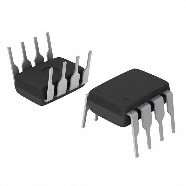
| 供应商器件封装 | 8-PDIP |
| 其它名称 | CAT24C512LI-G-ND |
| 包装 | 管件 |
| 商标 | ON Semiconductor |
| 存储器类型 | EEPROM |
| 存储容量 | 512K (64K x 8) |
| 安装风格 | Through Hole |
| 封装 | Tube |
| 封装/外壳 | 8-DIP(0.300",7.62mm) |
| 封装/箱体 | PDIP-8 |
| 工作温度 | -40°C ~ 85°C |
| 工作电流 | 2.5 mA |
| 工作电源电压 | 2.5 V, 3.3 V, 5 V |
| 工厂包装数量 | 50 |
| 接口 | I²C,2 线串口 |
| 接口类型 | Serial |
| 数据保留 | 100 yr |
| 最大工作温度 | + 85 C |
| 最大工作电流 | 5 uA |
| 最大时钟频率 | 400 kHz |
| 最小工作温度 | - 40 C |
| 标准包装 | 50 |
| 格式-存储器 | EEPROMs - 串行 |
| 电压-电源 | 1.8 V ~ 5.5 V |
| 电源电压-最大 | 5.5 V |
| 电源电压-最小 | 1.8 V |
| 系列 | CAT24C512 |
| 组织 | 64 k x 8 |
| 访问时间 | 900 ns |
| 速度 | 100kHz,400kHz,1MHz |


PDF Datasheet 数据手册内容提取
CAT24C512 EEPROM Serial 512-Kb I2C Description The CAT24C512 is a EERPOM Serial 512−Kb I2C internally organized as 65,536 words of 8 bits each. It features a 128−byte page write buffer and supports the Standard (100kHz), Fast (400 kHz) and Fast−Plus (1 MHz) I2C protocol. www.onsemi.com Write operations can be inhibited by taking the WP pin High (this protects the entire memory). External address pins make it possible to address up to eight CAT24C512 devices on the same bus. On−Chip ECC (Error Correction Code) makes the device suitable TSSOP−8 UDFN−8 SOIC−8 Y SUFFIX HU5 SUFFIX X SUFFIX for high reliability applications. CASE 948AL CASE 517BU CASE 751BE Features • Supports Standard, Fast and Fast−Plus I2C Protocol • 1.8 V to 5.5 V Supply Voltage Range • SOIC−8 SOIC−8 WIDE WLCSP−8 128−Byte Page Write Buffer • W SUFFIX X SUFFIX C8A SUFFIX Hardware Write Protection for Entire Memory CASE 751BD CASE 751BE CASE 567JL • Schmitt Triggers and Noise Suppression Filters on I2C Bus Inputs (SCL and SDA) • Low Power CMOS Technology • 1,000,000 Program/Erase Cycles PIN CONFIGURATIONS • Pin A1 100 Year Data Retention A0 VCC Reference • 1 Industrial and Extended Temperature Range A1 WP • 8−pin, SOIC, TSSOP, 8−pad UDFN and 8−ball WLCSP Packages • A2 SCL SDA VCC These Devices are Pb−Free, Halogen Free/BFR Free and are RoHS VSS SDA Compliant SCL SOIC (W, X), TSSOP (Y), A2 WP VCC UDFN (HU5) A1 (Top View) VSS A0 SCL For the location of Pin 1, please consult the corresponding WLCSP (C8A) A2, A1, A0 CAT24C512 SDA package drawing. (Top View) WP PIN FUNCTION Pin Name Function VSS A0, A1, A2 Device Address SDA Serial Data Figure 1. Functional Symbol SCL Serial Clock WP Write Protect VCC Power Supply VSS Ground ORDERING INFORMATION See detailed ordering and shipping information in the package dimensions section on page 10 of this data sheet. © Semiconductor Components Industries, LLC, 2015 1 Publication Order Number: May, 2018 − Rev. 8 CAT24C512/D
CAT24C512 MARKING DIAGRAMS 24512A = Specific Device Code A = Assembly Location Code 24512A Y = Production Year (Last Digit) AYMXXX M = Production Month (1−9, O, N, D) (cid:2) XXX = Last Three Digits of Assembly Lot Number (cid:2) = Pb−Free Microdot SOIC−8 (W, X) C9L = Specific Device Code C9L A = Assembly Location Code ALL LL = Last Two Digits of Assembly Lot Number YM Y = Production Year (Last Digit) (cid:2) M = Production Month (1−9, O, N, D) (cid:2) = Pb−Free Microdot UDFN−8 (HU5) C12A = Specific Device Code A = Assembly Location Code C12A Y = Production Year (Last Digit) AYMXXX M = Production Month (1−9, O, N, D) (cid:2) XXX = Last Three Digits of Assembly Lot Number (cid:2) = Pb−Free Microdot TSSOP−8 (Y) C9A C9A = Specific Device Code AYW A = Assembly Location Y = Production Year WLCSP (C8A) W = Production Week www.onsemi.com 2
CAT24C512 Table 1. ABSOLUTE MAXIMUM RATINGS Parameters Ratings Units Storage Temperature –65 to +150 °C Voltage on any Pin with Respect to Ground (Note 1) –0.5 to +6.5 V Stresses exceeding those listed in the Maximum Ratings table may damage the device. If any of these limits are exceeded, device functionality should not be assumed, damage may occur and reliability may be affected. 1. The DC input voltage on any pin should not be lower than −0.5 V or higher than VCC + 0.5 V. During transitions, the voltage on any pin may undershoot to no less than −1.5 V or overshoot to no more than VCC + 1.5 V, for periods of less than 20 ns. Table 2. RELIABILITY CHARACTERISTICS (Note 2) Symbol Parameter Min Units NEND (Notes 3, 4) Endurance 1,000,000 Program/Erase Cycles TDR Data Retention 100 Years 2. These parameters are tested initially and after a design or process change that affects the parameter according to appropriate AEC−Q100 and JEDEC test methods. 3. Page Mode, VCC = 5 V, 25°C. 4. The device uses ECC (Error Correction Code) logic with 6 ECC bits to correct one bit error in 4 data bytes. Therefore, when a single byte has to be written, 4 bytes (including the ECC bits) are re-programmed. It is recommended to write by multiple of 4 bytes in order to benefit from the maximum number of write cycles. Table 3. D.C. OPERATING CHARACTERISTICS VCC = 1.8 V to 5.5 V, TA = −40°C to +85°C and VCC = 2.5 V to 5.5 V, TA = −40°C to +125°C, unless otherwise specified. Symbol Parameter Test Conditions Min Max Units ICCR Read Current Read, fSCL = 400 kHz/1 MHz 1 mA ICCW Write Current VCC = 1.8 V 1.8 mA VCC = 5.5 V 2.5 ISB Standby Current All I/O Pins at GND or VCC TA = −40°C to +85°C 2 (cid:2)A TA = −40°C to +125°C 5 IL I/O Pin Leakage Pin at GND or VCC TA = −40°C to +85°C 1 (cid:2)A TA = −40°C to +125°C 2 VIL1 Input Low Voltage 2.5 V ≤ VCC ≤ 5.5 V −0.5 0.3 VCC V VIL2 Input Low Voltage 1.8 V ≤ VCC < 2.5 V −0.5 0.25 VCC V VIH1 Input High Voltage 2.5 V ≤ VCC ≤ 5.5 V 0.7 VCC VCC + 0.5 V VIH2 Input High Voltage 1.8 V ≤ VCC < 2.5 V 0.75 VCC VCC + 0.5 V VOL1 Output Low Voltage VCC ≥ 2.5 V, IOL = 3.0 mA 0.4 V VOL2 Output Low Voltage VCC < 2.5 V, IOL = 1.0 mA 0.2 V Product parametric performance is indicated in the Electrical Characteristics for the listed test conditions, unless otherwise noted. Product performance may not be indicated by the Electrical Characteristics if operated under different conditions. Table 4. PIN IMPEDANCE CHARACTERISTICS VCC = 1.8 V to 5.5 V, TA = −40°C to +85°C and VCC = 2.5 V to 5.5 V, TA = −40°C to +125°C, unless otherwise specified. Symbol Parameter Conditions Max Units CIN (Note 5) SDA I/O Pin Capacitance VIN = 0 V 8 pF CIN (Note 5) Input Capacitance (other pins) VIN = 0 V 6 pF IWP, IA (Note 6) WP Input Current, Address Input VIN < VIH, VCC = 5.5 V 75 (cid:2)A Current (A0, A1, A2) VIN < VIH, VCC = 3.3 V 50 VIN < VIH, VCC = 1.8 V 25 VIN > VIH 2 5. These parameters are tested initially and after a design or process change that affects the parameter according to appropriate AEC−Q100 and JEDEC test methods. 6. When not driven, the WP, A0, A1, A2 pins are pulled down to GND internally. For improved noise immunity, the internal pull−down is relatively strong; therefore the external driver must be able to supply the pull−down current when attempting to drive the input HIGH. To conserve power, as the input level exceeds the trip point of the CMOS input buffer (~ 0.5 x VCC), the strong pull−down reverts to a weak current source. www.onsemi.com 3
CAT24C512 Table 5. A.C. CHARACTERISTICS (Note 7) VCC = 1.8 V to 5.5 V, TA = −40°C to +85°C and VCC = 2.5 V to 5.5 V, TA = −40°C to +125°C, unless otherwise specified. Fast−Plus Standard Fast VCC = 2.5 V − 5.5 V VCC = 1.8 V − 5.5 V VCC = 1.8 V − 5.5 V TA = −40(cid:2)C to +85(cid:2)C Symbol Parameter Min Max Min Max Min Max Units FSCL Clock Frequency 100 400 1,000 kHz tHD:STA START Condition Hold Time 4 0.6 0.25 (cid:2)s tLOW Low Period of SCL Clock 4.7 1.3 0.45 (cid:2)s tHIGH High Period of SCL Clock 4 0.6 0.40 (cid:2)s tSU:STA START Condition Setup Time 4.7 0.6 0.25 (cid:2)s tHD:DAT Data In Hold Time 0 0 0 (cid:2)s tSU:DAT Data In Setup Time 250 100 50 ns tR (Note 8) SDA and SCL Rise Time 1,000 300 100 ns tF (Note 8) SDA and SCL Fall Time 300 300 100 ns tSU:STO STOP Condition Setup Time 4 0.6 0.25 (cid:2)s tBUF Bus Free Time Between 4.7 1.3 0.5 (cid:2)s STOP and START tAA SCL Low to Data Out Valid 3.5 0.9 0.40 (cid:2)s tDH Data Out Hold Time 50 50 50 ns Ti (Note 8) Noise Pulse Filtered at SCL 50 50 50 ns and SDA Inputs tSU:WP WP Setup Time 0 0 0 (cid:2)s tHD:WP WP Hold Time 2.5 2.5 1 (cid:2)s tWR Write Cycle Time 5 5 5 ms tPU (Notes 8, 9) Power-up to Ready Mode 1 1 0.1 1 ms 7. Test conditions according to “A.C. Test Conditions” table. 8. Tested initially and after a design or process change that affects this parameter. 9. tPU is the delay between the time VCC is stable and the device is ready to accept commands. Table 6. A.C. TEST CONDITIONS Input Levels 0.2 x VCC to 0.8 x VCC Input Rise and Fall Times ≤ 50 ns Input Reference Levels 0.3 x VCC, 0.7 x VCC Output Reference Levels 0.5 x VCC Output Load Current Source: IL = 3 mA (VCC ≥ 2.5 V); IL = 1 mA (VCC < 2.5 V); CL = 100 pF www.onsemi.com 4
CAT24C512 Power-On Reset (POR) device pulls down the SDA line to ‘transmit’ a ‘0’ and The CAT24C512 incorporates Power−On Reset (POR) releases it to ‘transmit’ a ‘1’. circuitry which protects the internal logic against powering Data transfer may be initiated only when the bus is not up in the wrong state. busy (see A.C. Characteristics). The device will power up into Standby mode after V During data transfer, the SDA line must remain stable CC exceeds the POR trigger level and will power down into while the SCL line is HIGH. An SDA transition while SCL Reset mode when V drops below the POR trigger level. is HIGH will be interpreted as a START or STOP condition CC (Figure2). This bi−directional POR behavior protects the device against brown−out failure, following a temporary loss of START power. The START condition precedes all commands. It consists of a HIGH to LOW transition on SDA while SCL is HIGH. Pin Description The START acts as a ‘wake−up’ call to all receivers. Absent SCL: The Serial Clock input pin accepts the Serial Clock a START, a Slave will not respond to commands. signal generated by the Master. SDA: The Serial Data I/O pin receives input data and STOP transmits data stored in EEPROM. In transmit mode, this pin The STOP condition completes all commands. It consists is open drain. Data is acquired on the positive edge, and is of a LOW to HIGH transition on SDA while SCL is HIGH. delivered on the negative edge of SCL. The STOP starts the internal Write cycle (when following a Write command) or sends the Slave into standby mode A , A and A : The Address pins accept the device address. 0 1 2 (when following a Read command). These pins have on−chip pull−down resistors. WP: The Write Protect input pin inhibits all write Device Addressing operations, when pulled HIGH. This pin has an on−chip The Master initiates data transfer by creating a START pull−down resistor. condition on the bus. The Master then broadcasts an 8−bit serial Slave address. The first 4 bits of the Slave address are Functional Description set to 1010, for normal Read/Write operations (Figure 3). The CAT24C512 supports the Inter−Integrated Circuit The next 3 bits, A , A and A , select one of 8 possible Slave 2 1 0 (I2C) Bus data transmission protocol, which defines a device devices. The last bit, R/W, specifies whether a Read (1) or that sends data to the bus as a transmitter and a device Write (0) operation is to be performed. receiving data as a receiver. Data flow is controlled by a Master device, which generates the serial clock and all Acknowledge START and STOP conditions. The CAT24C512 acts as a After processing the Slave address, the Slave responds Slave device. Master and Slave alternate as either with an acknowledge (ACK) by pulling down the SDA line transmitter or receiver. Up to 8 devices may be connected to during the 9th clock cycle (Figure 4). The Slave will also the bus as determined by the device address inputs A , A , acknowledge the byte address and every data byte presented 0 1 and A . in Write mode. In Read mode the Slave shifts out a data byte, 2 and then releases the SDA line during the 9th clock cycle. If I2C Bus Protocol the Master acknowledges the data, then the Slave continues The I2C bus consists of two ‘wires’, SCL and SDA. The transmitting. The Master terminates the session by not two wires are connected to the V supply via pull−up CC acknowledging the last data byte (NoACK) and by sending resistors. Master and Slave devices connect to the 2−wire a STOP to the Slave. Bus timing is illustrated in Figure 5. bus via their respective SCL and SDA pins. The transmitting www.onsemi.com 5
CAT24C512 SCL SDA START STOP CONDITION CONDITION Figure 2. Start/Stop Timing 1 0 1 0 A2 A1 A0 R/W DEVICE ADDRESS Figure 3. Slave Address Bits BUS RELEASE DELAY (TRANSMITTER) BUS RELEASE DELAY (RECEIVER) SCL FROM 1 8 9 MASTER DATA OUTPUT FROM TRANSMITTER DATA OUTPUT FROM RECEIVER START ACK SETUP (≥ tSU:DAT) ACK DELAY (≤ tAA) Figure 4. Acknowledge Timing tF tHIGH tR tLOW tLOW SCL tSU:STA tHD:DAT tHD:STA tSU:DAT tSU:STO SDA IN tAA tDH tBUF SDA OUT Figure 5. Bus Timing www.onsemi.com 6
CAT24C512 WRITE OPERATIONS Acknowledge Polling Acknowledge polling can be used to determine if the Byte Write CAT24C512 is busy writing or is ready to accept commands. In Byte Write mode the Master sends a START, followed Polling is implemented by interrogating the device with a by Slave address, two byte address and data to be written ‘Selective Read’ command (see READ OPERATIONS). (Figure6). The Slave acknowledges all 4 bytes, and the The CAT24C512 will not acknowledge the Slave address, Master then follows up with a STOP, which in turn starts the as long as internal Write is in progress. internal Write operation (Figure 7). During internal Write, the Slave will not acknowledge any Read or Write request Hardware Write Protection from the Master. With the WP pin held HIGH, the entire memory is protected against Write operations. If the WP pin is left Page Write floating or is grounded, it has no impact on the operation of The CAT24C512 contains 65,536 bytes of data, arranged the CAT24C512. The state of the WP pin is strobed on the in 512 pages of 128 bytes each. A two byte address word, last falling edge of SCL immediately preceding the first data following the Slave address, points to the first byte to be byte (Figure 9). If the WP pin is HIGH during the strobe written. The most significant 9 bits (A to A ) identify the 15 7 interval, the CAT24C512 will not acknowledge the data byte page and the last 7 bits identify the byte within the page. Up and the Write request will be rejected. to 128 bytes can be written in one Write cycle (Figure 8). The internal byte address counter is automatically Delivery State incremented after each data byte is loaded. If the Master The CAT24C512 is shipped erased, i.e., all bytes are FFh. transmits more than 128 data bytes, then earlier bytes will be overwritten by later bytes in a ‘wrap−around’ fashion (within the selected page). The internal Write cycle starts immediately following the STOP. www.onsemi.com 7
CAT24C512 S T S BUS ACTIVITY: A SLAVE BYTE ADDRESS T MASTER RT ADDRESS A15 − A8 A7 − A0 DATA OP SDA LINE S P A A A A C C C C K K K K Figure 6. Byte Write Timing SCL SDA 8th Bit ACK Byte n tWR STOP START ADDRESS CONDITION CONDITION Figure 7. Write Cycle Timing S BUS T S ACTIVITY: A SLAVE BYTE ADDRESS T MASTER RT ADDRESS A15 − A8 A7 − A0 DATA DATA n DATA n+127 OP SDA LINE S P A A A A A A A C C C C C C C K K K K K K K Figure 8. Page Write Timing ADDRESS DATA BYTE BYTE 1 8 9 1 8 SCL SDA a7 a0 d7 d0 tSU:WP WP tHD:WP Figure 9. WP Timing www.onsemi.com 8
CAT24C512 READ OPERATIONS The address counter can be initialized by performing a ‘dummy’ Write operation (Figure 11). Here the START is Immediate Address Read followed by the Slave address (with the R/W bit set to ‘0’) In standby mode, the CAT24C512 internal address and the desired two byte address. Instead of following up counter points to the data byte immediately following the with data, the Master then issues a 2nd START, followed by last byte accessed by a previous operation. If that ‘previous’ the ‘Immediate Address Read’ sequence, as described byte was the last byte in memory, then the address counter earlier. will point to the 1st memory byte, etc. When, following a START, the CAT24C512 is presented Sequential Read with a Slave address containing a ‘1’ in the R/W bit position If the Master acknowledges the 1st data byte transmitted (Figure10), it will acknowledge (ACK) in the 9th clock cycle, by the CAT24C512, then the device will continue and will then transmit data being pointed at by the internal transmitting as long as each data byte is acknowledged by address counter. The Master can stop further transmission by the Master (Figure 12). If the end of memory is reached issuing a NoACK, followed by a STOP condition. during sequential Read, then the address counter will ‘wrap−around’ to the beginning of memory, etc. Sequential Selective Read Read works with either ‘Immediate Address Read’ or The Read operation can also be started at an address ‘Selective Read’, the only difference being the starting byte different from the one stored in the internal address counter. address. S T S BUS ACTIVITY: A SLAVE T MASTER R ADDRESS O T P SDA LINE S P A N C DATA O K A C K SCL 8 9 SDA 8th Bit DATA OUT NO ACK STOP Figure 10. Immediate Address Read Timing S S T T S BUS ACTIVITY: A SLAVE BYTE ADDRESS A SLAVE T MASTER RT ADDRESS A15 − A8 A7 − A0 RT ADDRESS DATA OP SDA LINE S S P A A A A N C C C C O K K K K A C Figure 11. Selective Read Timing K S BUS ACTIVITY: SLAVE T MASTER ADDRESS DATA n DATA n+1 DATA n+2 DATA n+x O P SDA LINE P A A A A N C C C C O K K K K A C K Figure 12. Sequential Read Timing www.onsemi.com 9
CAT24C512 ORDERING INFORMATION (Notes 10, 11) Specific Device Lead Device Order Number Marking Package Type Temperature Range Finish Shipping† CAT24C512WI−GT3 24512A SOIC−8, JEDEC −40°C to +85°C NiPdAu Tape & Reel, 3,000 Units / Reel CAT24C512XI−T2 24512A SOIC−8, EIAJ −40°C to +85°C Matte−Tin Tape & Reel, 2,000 Units / Reel CAT24C512YI−GT3 C12A TSSOP−8 −40°C to +85°C NiPdAu Tape & Reel, 3,000 Units / Reel CAT24C512HU5EGT3 C9L UDFN8 −40°C to +125°C NiPdAu Tape & Reel, 3,000 Units / Reel CAT24C512HU5IGT3 C9L UDFN8 −40°C to +85°C NiPdAu Tape & Reel, 3,000 Units / Reel CAT24C512C8ATR C9A WLCSP−8 −40°C to +85°C SnAgCu Tape & Reel, 5,000 Units / Reel †For information on tape and reel specifications, including part orientation and tape sizes, please refer to our Tape and Reel Packaging Specifications Brochure, BRD8011/D. 10.All packages are RoHS-compliant (Lead-free, Halogen-free). 11.For detailed information and a breakdown of device nomenclature and numbering systems, please see the ON Semiconductor Device Nomenclature document, TND310/D, availablse at www.onsemi.com ON Semiconductor is licensed by the Philips Corporation to carry the I2C bus protocol. www.onsemi.com 10
MECHANICAL CASE OUTLINE PACKAGE DIMENSIONS UDFN8 3.0x2.0, 0.5P CASE 517BU−01 ISSUE O DATE 06 APR 2011 SCALE 4:1 D A B NOTES: 1. DIMENSIONING AND TOLERANCING PER ASME Y14.5M, 1994. (0.065) 2. CONTROLLING DIMENSION: MILLIMETERS. 3. DIMENSIONS b APPLIES TO PLATED ÍÍÍ TERMINAL AND IS MEASURED BETWEEN E 0.15 AND 0.25 MM FROM TERMINAL TIP. REFEREPNINC 1E ÍÍÍ (0.127) 4. CPAODP LAASN WAREILTLY A ASP TPHLEIE TSE TROM TINHAEL ESX.POSED DETAIL A ÍÍÍ MILLIMETERS 0.15 C DIM MIN MAX A 0.45 0.55 A1 0.00 0.05 0.15 C TOP VIEW b 0.20 0.30 D 2.00 BSC D2 1.35 1.45 DETAIL A E 3.00 BSC 0.05 C E2 0.85 0.95 A e 0.50 BSC L 0.35 0.45 0.05 C A1 NOTE 4 GENERIC SIDE VIEW C SPELAATNIENG MARKING DIAGRAM* 0.10 M C A B XXX D2 ALL 8XL YM 1 4 (cid:2) 0.10 M C A B XXX= Specific Device Code A = Assembly Location Code LL = Assembly Lot E2 Y = Year M = Month 8 5 (cid:2) = Pb−Free Package 8Xb e 0.10 M C A B *This information is generic. Please refer to device data sheet for actual part marking. BOTTOM VIEW 0.05 M C D NOTE 3 Pb−Free indicator, “G” or microdot “ (cid:2)”, may or may not be present. RECOMMENDED MOUNTING FOOTPRINT 1.56 8X0.63 1.06 3.30 PKG OUTLINE 1 8X 0.32 0.50 PITCH DIMENSIONS: MILLIMETERS Electronic versions are uncontrolled except when accessed directly from the Document Repository. DOCUMENT NUMBER: 98AON55336E Printed versions are uncontrolled except when stamped “CONTROLLED COPY” in red. DESCRIPTION: UDFN8 3.0 X 2.0, 0.5P PAGE 1 OF 1 ON Semiconductor and are trademarks of Semiconductor Components Industries, LLC dba ON Semiconductor or its subsidiaries in the United States and/or other countries. ON Semiconductor reserves the right to make changes without further notice to any products herein. ON Semiconductor makes no warranty, representation or guarantee regarding the suitability of its products for any particular purpose, nor does ON Semiconductor assume any liability arising out of the application or use of any product or circuit, and specifically disclaims any and all liability, including without limitation special, consequential or incidental damages. ON Semiconductor does not convey any license under its patent rights nor the rights of others. © Semiconductor Components Industries, LLC, 2019 www.onsemi.com
MECHANICAL CASE OUTLINE PACKAGE DIMENSIONS SOIC 8, 150 mils CASE 751BD−01 ISSUE O DATE 19 DEC 2008 SYMBOL MIN NOM MAX A 1.35 1.75 A1 0.10 0.25 b 0.33 0.51 c 0.19 0.25 E1 E D 4.80 5.00 E 5.80 6.20 E1 3.80 4.00 e 1.27 BSC h 0.25 0.50 L 0.40 1.27 PIN # 1 IDENTIFICATION θ 0º 8º TOP VIEW D h A1 θ A c e b L SIDE VIEW END VIEW Notes: (1) All dimensions are in millimeters. Angles in degrees. (2) Complies with JEDEC MS-012. DOCUMENT NUMBER: 98AON34272E Electronic versions are uncontrolled except when accessed directly from the Document Repository. Printed STATUS: ON SEMICONDUCTOR STANDARD versions are uncontrolled except when stamped “CONTROLLED COPY” in red. REFERENCE: © Semiconductor Components Industries, LLC, 2002 http://onsemi.com Case Outline Number: October, D20E0S2C −R RIePvT. I0ON: SOIC 8, 150 MILS 1 PAGE 1 OFX 2XX
DOCUMENT NUMBER: 98AON34272E PAGE 2 OF 2 ISSUE REVISION DATE O RELEASED FOR PRODUCTION FROM POD #SOIC8−002−01 TO ON 19 DEC 2008 SEMICONDUCTOR. REQ. BY B. BERGMAN. ON Semiconductor and are registered trademarks of Semiconductor Components Industries, LLC (SCILLC). SCILLC reserves the right to make changes without further notice to any products herein. SCILLC makes no warranty, representation or guarantee regarding the suitability of its products for any particular purpose, nor does SCILLC assume any liability arising out of the application or use of any product or circuit, and specifically disclaims any and all liability, including without limitation special, consequential or incidental damages. “Typical” parameters which may be provided in SCILLC data sheets and/or specifications can and do vary in different applications and actual performance may vary over time. All operating parameters, including “Typicals” must be validated for each customer application by customer’s technical experts. SCILLC does not convey any license under its patent rights nor the rights of others. SCILLC products are not designed, intended, or authorized for use as components in systems intended for surgical implant into the body, or other applications intended to support or sustain life, or for any other application in which the failure of the SCILLC product could create a situation where personal injury or death may occur. Should Buyer purchase or use SCILLC products for any such unintended or unauthorized application, Buyer shall indemnify and hold SCILLC and its officers, employees, subsidiaries, affiliates, and distributors harmless against all claims, costs, damages, and expenses, and reasonable attorney fees arising out of, directly or indirectly, any claim of personal injury or death associated with such unintended or unauthorized use, even if such claim alleges that SCILLC was negligent regarding the design or manufacture of the part. SCILLC is an Equal Opportunity/Affirmative Action Employer. This literature is subject to all applicable copyright laws and is not for resale in any manner. © Semiconductor Components Industries, LLC, 2008 Case Outline Number: December, 2008 − Rev. 01O 751BD
MECHANICAL CASE OUTLINE PACKAGE DIMENSIONS SOIC−8, 208 mils CASE 751BE−01 ISSUE O DATE 19 DEC 2008 SYMBOL MIN NOM MAX A 2.03 A1 0.05 0.25 b 0.36 0.48 c 0.19 0.25 E1 E D 5.13 5.33 E 7.75 8.26 E1 5.13 5.38 e 1.27 BSC L 0.51 0.76 θ 0º 8º PIN#1 IDENTIFICATION TOP VIEW D A (cid:2) e b L c A1 SIDE VIEW END VIEW Notes: (1) All dimensions are in millimeters. Angles in degrees. (2) Complies with EIAJ EDR-7320. DOCUMENT NUMBER: 98AON34273E Electronic versions are uncontrolled except when accessed directly from the Document Repository. Printed STATUS: ON SEMICONDUCTOR STANDARD versions are uncontrolled except when stamped “CONTROLLED COPY” in red. REFERENCE: © Semiconductor Components Industries, LLC, 2002 http://onsemi.com Case Outline Number: October, D20E0S2C −R RIePvT. I0ON: SOIC−8, 208 MILS 1 PAGE 1 OFX 2XX
DOCUMENT NUMBER: 98AON34273E PAGE 2 OF 2 ISSUE REVISION DATE O RELEASED FOR PRODUCTION FROM POD #SOIK8−031−01 TO ON 19 DEC 2008 SEMICONDUCTOR. REQ. BY B. BERGMAN. ON Semiconductor and are registered trademarks of Semiconductor Components Industries, LLC (SCILLC). SCILLC reserves the right to make changes without further notice to any products herein. SCILLC makes no warranty, representation or guarantee regarding the suitability of its products for any particular purpose, nor does SCILLC assume any liability arising out of the application or use of any product or circuit, and specifically disclaims any and all liability, including without limitation special, consequential or incidental damages. “Typical” parameters which may be provided in SCILLC data sheets and/or specifications can and do vary in different applications and actual performance may vary over time. All operating parameters, including “Typicals” must be validated for each customer application by customer’s technical experts. SCILLC does not convey any license under its patent rights nor the rights of others. SCILLC products are not designed, intended, or authorized for use as components in systems intended for surgical implant into the body, or other applications intended to support or sustain life, or for any other application in which the failure of the SCILLC product could create a situation where personal injury or death may occur. Should Buyer purchase or use SCILLC products for any such unintended or unauthorized application, Buyer shall indemnify and hold SCILLC and its officers, employees, subsidiaries, affiliates, and distributors harmless against all claims, costs, damages, and expenses, and reasonable attorney fees arising out of, directly or indirectly, any claim of personal injury or death associated with such unintended or unauthorized use, even if such claim alleges that SCILLC was negligent regarding the design or manufacture of the part. SCILLC is an Equal Opportunity/Affirmative Action Employer. This literature is subject to all applicable copyright laws and is not for resale in any manner. © Semiconductor Components Industries, LLC, 2008 Case Outline Number: December, 2008 − Rev. 01O 751BE
MECHANICAL CASE OUTLINE PACKAGE DIMENSIONS TSSOP8, 4.4x3 CASE 948AL−01 ISSUE O DATE 19 DEC 2008 b SYMBOL MIN NOM MAX A 1.20 A1 0.05 0.15 A2 0.80 0.90 1.05 b 0.19 0.30 E1 E c 0.09 0.20 D 2.90 3.00 3.10 E 6.30 6.40 6.50 E1 4.30 4.40 4.50 e 0.65 BSC L 1.00 REF L1 0.50 0.60 0.75 θ 0º 8º e TOP VIEW D A2 A (cid:2)1 c A1 L1 L SIDE VIEW END VIEW Notes: (1) All dimensions are in millimeters. Angles in degrees. (2) Complies with JEDEC MO-153. DOCUMENT NUMBER: 98AON34428E Electronic versions are uncontrolled except when accessed directly from the Document Repository. Printed STATUS: ON SEMICONDUCTOR STANDARD versions are uncontrolled except when stamped “CONTROLLED COPY” in red. REFERENCE: © Semiconductor Components Industries, LLC, 2002 http://onsemi.com Case Outline Number: October, D20E0S2C −R RIePvT. I0ON: TSSOP8, 4.4X3 1 PAGE 1 OFX 2XX
DOCUMENT NUMBER: 98AON34428E PAGE 2 OF 2 ISSUE REVISION DATE O RELEASED FOR PRODUCTION FROM POD #TSSOP8−004−01 TO ON 19 DEC 2008 SEMICONDUCTOR. REQ. BY B. BERGMAN. ON Semiconductor and are registered trademarks of Semiconductor Components Industries, LLC (SCILLC). SCILLC reserves the right to make changes without further notice to any products herein. SCILLC makes no warranty, representation or guarantee regarding the suitability of its products for any particular purpose, nor does SCILLC assume any liability arising out of the application or use of any product or circuit, and specifically disclaims any and all liability, including without limitation special, consequential or incidental damages. “Typical” parameters which may be provided in SCILLC data sheets and/or specifications can and do vary in different applications and actual performance may vary over time. All operating parameters, including “Typicals” must be validated for each customer application by customer’s technical experts. SCILLC does not convey any license under its patent rights nor the rights of others. SCILLC products are not designed, intended, or authorized for use as components in systems intended for surgical implant into the body, or other applications intended to support or sustain life, or for any other application in which the failure of the SCILLC product could create a situation where personal injury or death may occur. Should Buyer purchase or use SCILLC products for any such unintended or unauthorized application, Buyer shall indemnify and hold SCILLC and its officers, employees, subsidiaries, affiliates, and distributors harmless against all claims, costs, damages, and expenses, and reasonable attorney fees arising out of, directly or indirectly, any claim of personal injury or death associated with such unintended or unauthorized use, even if such claim alleges that SCILLC was negligent regarding the design or manufacture of the part. SCILLC is an Equal Opportunity/Affirmative Action Employer. This literature is subject to all applicable copyright laws and is not for resale in any manner. © Semiconductor Components Industries, LLC, 2008 Case Outline Number: December, 2008 − Rev. 01O 948AL
MECHANICAL CASE OUTLINE PACKAGE DIMENSIONS WLCSP8, 1.39x1.65 CASE 567JL ISSUE B SCALE 4:1 DATE 06 MAY 2015 E A B PIN A1 ÈÈ N1O.TDEISM:ENSIONING AND TOLERANCING PER REFERENCE ASME Y14.5M, 1994. ÈÈ 2. CONTROLLING DIMENSION: MILLIMETERS. 3. COPLANARITY APPLIES TO THE SPHERICAL D CROWNS OF THE SOLDER BALLS. 4. DATUM C, THE SEATING PLANE, IS DEFINED BY THE SPHERICAL CROWNS OF THE SOL- 2X 0.10 C DER BALLS. 5. DIMENSION b IS MEASURED AT THE MAXIMUM SOLDER BALL DIAMETER PARALLEL TO DA- 2X 0.10 C TOP VIEW TUM C. MILLIMETERS A2 DIM MIN MAX A −−− 0.60 0.10 C A A1 0.16 0.22 A2 0.35 REF b 0.22 0.32 D 1.39 BSC 0.08 C E 1.65 BSC A1 NOTE 3 SIDE VIEW C SPELAATNIENG ee1 00..45303 BBSSCC GENERIC e/2 e MARKING DIAGRAM* 8X b e1 XXX 0.05 C A B AYW 0.03 C C B XXX= Specific Device Code A = Assembly Location A Y = Year 1 2 3 4 5 W = Work Week BOTTOM VIEW *This information is generic. Please refer to device data sheet for actual part marking. Pb−Free indicator, “G” or microdot “ (cid:2)”, may or may not be present. RECOMMENDED SOLDERING FOOTPRINT* 0.500 PITCH 0.433 A1 PITCH PACKAGE OUTLINE 8X 0.27 0.25 PITCH DIMENSIONS: MILLIMETERS *For additional information on our Pb−Free strategy and soldering details, please download the ON Semiconductor Soldering and Mounting Techniques Reference Manual, SOLDERRM/D. DOCUMENT NUMBER: 98AON80360F Electronic versions are uncontrolled except when accessed directly from the Document Repository. Printed STATUS: ON SEMICONDUCTOR STANDARD versions are uncontrolled except when stamped “CONTROLLED COPY” in red. REFERENCE: © Semiconductor Components Industries, LLC, 2002 http://onsemi.com Case Outline Number: October, D20E0S2C −R RIePvT. I0ON: WLCSP8, 1.39X1.65 1 PAGE 1 OFX 2XX
DOCUMENT NUMBER: 98AON80360F PAGE 2 OF 2 ISSUE REVISION DATE O RELEASED FOR PRODUCTION. REQ. BY V. CRACIUNOIU 03 JAN 2014 A CHANGED PACKAGE DIMENSIONS FROM 1.38X1.64 TO 1.39X1.65X0.60. REQ. 10 APR 2015 BY E. IONESCU. B CORRECTED MARKING DIAGRAM CODE INFORMATION. REQ. BY E. IONESCU. 06 MAY 2015 ON Semiconductor and are registered trademarks of Semiconductor Components Industries, LLC (SCILLC). SCILLC reserves the right to make changes without further notice to any products herein. SCILLC makes no warranty, representation or guarantee regarding the suitability of its products for any particular purpose, nor does SCILLC assume any liability arising out of the application or use of any product or circuit, and specifically disclaims any and all liability, including without limitation special, consequential or incidental damages. “Typical” parameters which may be provided in SCILLC data sheets and/or specifications can and do vary in different applications and actual performance may vary over time. All operating parameters, including “Typicals” must be validated for each customer application by customer’s technical experts. SCILLC does not convey any license under its patent rights nor the rights of others. SCILLC products are not designed, intended, or authorized for use as components in systems intended for surgical implant into the body, or other applications intended to support or sustain life, or for any other application in which the failure of the SCILLC product could create a situation where personal injury or death may occur. Should Buyer purchase or use SCILLC products for any such unintended or unauthorized application, Buyer shall indemnify and hold SCILLC and its officers, employees, subsidiaries, affiliates, and distributors harmless against all claims, costs, damages, and expenses, and reasonable attorney fees arising out of, directly or indirectly, any claim of personal injury or death associated with such unintended or unauthorized use, even if such claim alleges that SCILLC was negligent regarding the design or manufacture of the part. SCILLC is an Equal Opportunity/Affirmative Action Employer. This literature is subject to all applicable copyright laws and is not for resale in any manner. © Semiconductor Components Industries, LLC, 2015 Case Outline Number: May, 2015 − Rev. B 567JL
ON Semiconductor and are trademarks of Semiconductor Components Industries, LLC dba ON Semiconductor or its subsidiaries in the United States and/or other countries. ON Semiconductor owns the rights to a number of patents, trademarks, copyrights, trade secrets, and other intellectual property. A listing of ON Semiconductor’s product/patent coverage may be accessed at www.onsemi.com/site/pdf/Patent−Marking.pdf. ON Semiconductor reserves the right to make changes without further notice to any products herein. ON Semiconductor makes no warranty, representation or guarantee regarding the suitability of its products for any particular purpose, nor does ON Semiconductor assume any liability arising out of the application or use of any product or circuit, and specifically disclaims any and all liability, including without limitation special, consequential or incidental damages. Buyer is responsible for its products and applications using ON Semiconductor products, including compliance with all laws, regulations and safety requirements or standards, regardless of any support or applications information provided by ON Semiconductor. “Typical” parameters which may be provided in ON Semiconductor data sheets and/or specifications can and do vary in different applications and actual performance may vary over time. All operating parameters, including “Typicals” must be validated for each customer application by customer’s technical experts. ON Semiconductor does not convey any license under its patent rights nor the rights of others. ON Semiconductor products are not designed, intended, or authorized for use as a critical component in life support systems or any FDA Class 3 medical devices or medical devices with a same or similar classification in a foreign jurisdiction or any devices intended for implantation in the human body. Should Buyer purchase or use ON Semiconductor products for any such unintended or unauthorized application, Buyer shall indemnify and hold ON Semiconductor and its officers, employees, subsidiaries, affiliates, and distributors harmless against all claims, costs, damages, and expenses, and reasonable attorney fees arising out of, directly or indirectly, any claim of personal injury or death associated with such unintended or unauthorized use, even if such claim alleges that ON Semiconductor was negligent regarding the design or manufacture of the part. ON Semiconductor is an Equal Opportunity/Affirmative Action Employer. This literature is subject to all applicable copyright laws and is not for resale in any manner. PUBLICATION ORDERING INFORMATION LITERATURE FULFILLMENT: N. American Technical Support: 800−282−9855 Toll Free ON Semiconductor Website: www.onsemi.com Literature Distribution Center for ON Semiconductor USA/Canada 19521 E. 32nd Pkwy, Aurora, Colorado 80011 USA Europe, Middle East and Africa Technical Support: Order Literature: http://www.onsemi.com/orderlit Phone: 303−675−2175 or 800−344−3860 Toll Free USA/Canada Phone: 421 33 790 2910 Fax: 303−675−2176 or 800−344−3867 Toll Free USA/Canada For additional information, please contact your local Email: orderlit@onsemi.com Sales Representative ◊
Mouser Electronics Authorized Distributor Click to View Pricing, Inventory, Delivery & Lifecycle Information: O N Semiconductor: CAT24C512XI-T2 CAT24C512LI-G CAT24C512WI-GT3 CAT24C512YI-GT3 CAT24C512HU5IGT3 CAT24C512YI- G CAT24C512YIGT3JN