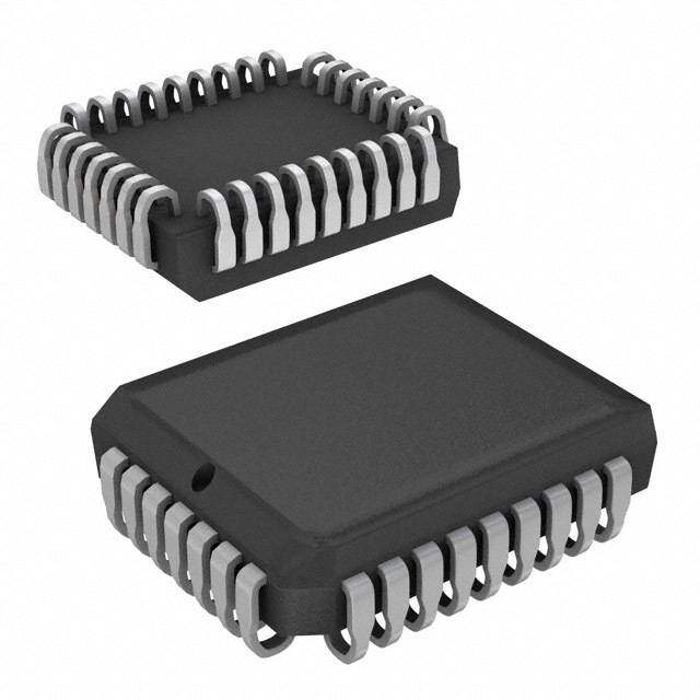
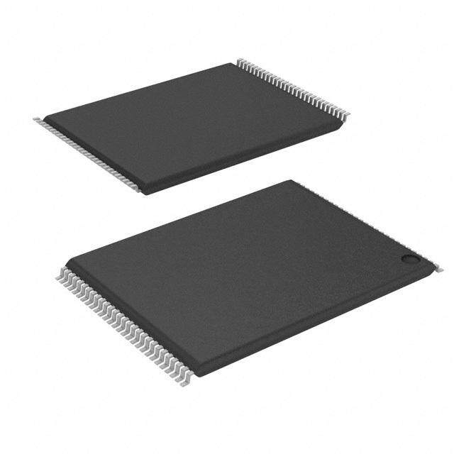
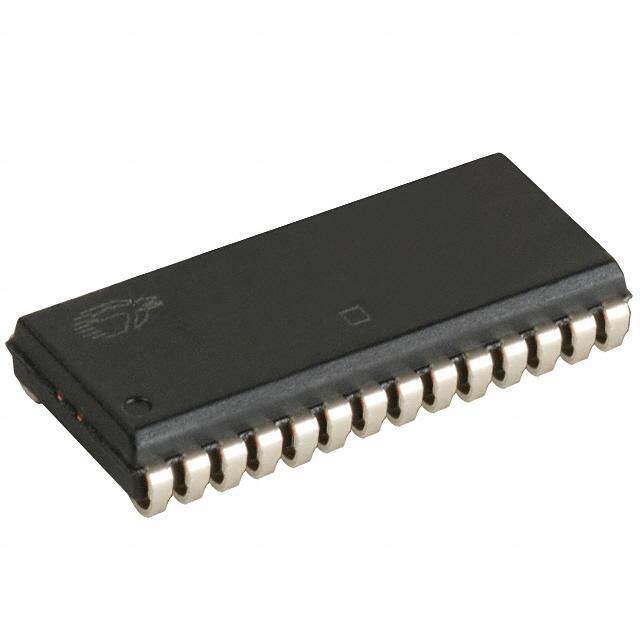
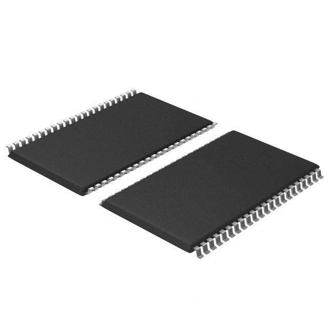
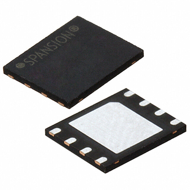
- 型号: CAT24C208WI-GT3
- 制造商: ON Semiconductor
- 库位|库存: xxxx|xxxx
- 要求:
| 数量阶梯 | 香港交货 | 国内含税 |
| +xxxx | $xxxx | ¥xxxx |
查看当月历史价格
查看今年历史价格
CAT24C208WI-GT3产品简介:
ICGOO电子元器件商城为您提供CAT24C208WI-GT3由ON Semiconductor设计生产,在icgoo商城现货销售,并且可以通过原厂、代理商等渠道进行代购。 CAT24C208WI-GT3价格参考。ON SemiconductorCAT24C208WI-GT3封装/规格:存储器, EEPROM 存储器 IC 8Kb (256 x 8 x 4) I²C 400kHz 900ns 8-SOIC。您可以下载CAT24C208WI-GT3参考资料、Datasheet数据手册功能说明书,资料中有CAT24C208WI-GT3 详细功能的应用电路图电压和使用方法及教程。
| 参数 | 数值 |
| 产品目录 | 集成电路 (IC) |
| 描述 | IC EEPROM 8KBIT 400KHZ 8SOIC |
| 产品分类 | |
| 品牌 | ON Semiconductor |
| 数据手册 | |
| 产品图片 |
|
| 产品型号 | CAT24C208WI-GT3 |
| rohs | 无铅 / 符合限制有害物质指令(RoHS)规范要求 |
| 产品系列 | - |
| 供应商器件封装 | 8-SOIC |
| 其它名称 | CAT24C208WI-GT3OSCT |
| 包装 | 剪切带 (CT) |
| 存储器类型 | EEPROM |
| 存储容量 | 8K (4 x 256 x 8) |
| 封装/外壳 | 8-SOIC(0.154",3.90mm 宽) |
| 工作温度 | -40°C ~ 85°C |
| 接口 | I²C,2 线串口 |
| 标准包装 | 1 |
| 格式-存储器 | EEPROMs - 串行 |
| 电压-电源 | 2.5 V ~ 5.5 V |
| 速度 | 400kHz |


PDF Datasheet 数据手册内容提取
CAT24C208 EEPROM Serial 8-Kb I2C Dual Port Description The CAT24C208 is an EEPROM Serial 8−Kb I2C Dual Port internally organized as 4 segments of 256 bytes each. The www.onsemi.com CAT24C208 features a 16−byte page write buffer and can be accessed from either of two separate I2C compatible ports, DSP (SDA, SCL) and DDC (SDA, SCL). Arbitration between the two interface ports is automatic and allows the appearance of individual access to the memory from each SOIC−8 interface. W SUFFIX CASE 751BD Features • Supports Standard and Fast I2C Protocol • PIN CONFIGURATION 2.5 V to 5.5 V Operation • 16−Byte Page Write Buffer DSP VCC 1 DDC VCC • Schmitt Triggers and Noise Protection Filters on I2C Bus Input DSP SCL EDID SEL • Low Power CMOS Technology DSP SDA DDC SCL • 1,000,000 Program/Erase Cycles VSS DDC SDA • 100 Year Data Retention SOIC (W) • Industrial Temperature Range (Top View) • SOIC 8−lead Package • This Device is Pb−Free, Halogen Free/BFR Free, and RoHS ORDERING INFORMATION Compliant See detailed ordering and shipping information in the package dimensions section on page 8 of this data sheet. DSP VCC DDC VCC ARBITRATION LOGIC D D E E C C 1K X 8 DSP SCL DISPLAY O O DDC DDC SCL CONTROL D MEMORY D CONTROL DSP SDA LOGIC E ARRAY E LOGIC DDC SDA R R S S CONFIGURATION EDID SEL VSS REGISTER Figure 1. Block Diagram © Semiconductor Components Industries, LLC, 2009 1 Publication Order Number: May, 2018 − Rev. 7 CAT24C208/D
CAT24C208 Table 1. PIN DESCRIPTION Pin Number Pin Name Function 1 DSP VCC Device power from display controller 2 DSP SCL The CAT24C208 DSP serial clock bidirectional pin is used to clock all data transfers into or out of the device DSP SDA pin and is also used to block DSP Port access when DDC Port is active. 3 DSP SDA DSP Serial Data/Address. The bidirectional DSP serial data/address pin is used to transfer data into and out of the device from a display controller. The DSP SDA pin is an open drain output and can be wireOR’ed with other open drain or open collector outputs. 4 VSS Device ground. 5 DDC SDA DDC Serial Data/Address. The bidirectional DDC serial data/address pin is used to transfer data into and out of the device from a DDC host. The DDC SDA pin is an open drain output and can be wire− OR’ed with other open drain or open collector outputs. 6 DDC SCL The CAT24C208 DDC serial clock bidirectional pin is used to clock all data transfers into or out of the device DDC SDA pin, and is used to block DDC Port for access when DSP Port is active. 7 EDID SEL EDID select. The CAT24C208 EDID select input selects the active bank of memory to be accessed via the DDC SDA/SCL interface as set in the configuration register. 8 DDC VCC Device power when powered from a DDC host. Table 2. ABSOLUTE MAXIMUM RATINGS Parameters Ratings Units Temperature Under Bias –55 to +125 °C Storage Temperature –65 to +150 °C Voltage on Any Pin with Respect to Ground (Note 1) –2.0 to +VCC +2.0 V VCC with Respect to Ground –2.0 to +7.0 V Package Power Dissipation Capability (TA = 25°C) 1.0 W Lead Soldering Temperature (10 secs) 300 °C Output Short Circuit Current (Note 2) 100 mA Stresses exceeding those listed in the Maximum Ratings table may damage the device. If any of these limits are exceeded, device functionality should not be assumed, damage may occur and reliability may be affected. 1. The minimum DC input voltage is –0.5 V. During transitions, inputs may undershoot to –2.0 V for periods of less than 20 ns. Maximum DC voltage on output pins is VCC + 0.5 V, which may overshoot to VCC + 2.0 V for periods of less than 20 ns. 2. Output shorted for no more than one second. No more than one output shorted at a time. Table 3. RELIABILITY CHARACTERISTICS Symbol Parameter Reference Test Method Min Units NEND (Note 3) Endurance MIL−STD−883, Test Method 1033 1,000,000 Cycles/Byte TDR (Note 3) Data Retention MIL−STD−883, Test Method 1008 100 Years VZAP (Note 3) ESD Susceptibility JEDEC Standard JESD 22 2000 Volts ILTH (Notes 3 and 4) Latch−up JEDEC Standard 17 100 mA 3. This parameter is tested initially and after a design or process change that affects the parameter. 4. Latch−up protection is provided for stresses up to 100 mA on address and data pins from –1 V to VCC +1 V. Table 4. CAPACITANCE (TA = 25°C, f = 1.0 MHz, VCC = 5 V) Symbol Parameter Conditions Min Typ Max Units CI/O (Note 5) Input/Output Capacitance (Either DSP or DDC SDA) VI/O = 0 V 8 pF CIN (Note 5) Input Capacitance (EDID, Either DSP or DDC SCL) VIN = 0 V 6 pF 5. This parameter is tested initially and after a design or process change that affects the parameter. www.onsemi.com 2
CAT24C208 Table 5. D.C. OPERATING CHARACTERISTICS (VCC = 2.5 V to 5.5 V, unless otherwise specified.) Symbol Parameter Test Conditions Min Typ Max Units ICC Power Supply Current fSCL = 100 KHz 3 mA ISB Standby Current (VCC = 5.0 V) VIN = GND or either DSP or DDC VCC 50 (cid:2)A ILI Input Leakage Current VIN = GND to either DSP or DDC VCC 10 (cid:2)A ILO Output Leakage Current VOUT = GND to either DSP or DDC VCC 10 (cid:2)A VIL Input Low Voltage −1 VCC x 0.3 V VIH Input High Voltage VCC x 0.7 VCC + 0.5 V VHYS Input Hysteresis 0.05 V VOL1 Output Low Voltage (VCC = 3 V) IOL = 3 mA 0.4 V VCCL1 Leakage DSP VCC to DDC VCC ±100 (cid:2)A VCCL2 Leakage DDC VCC to DSP VCC ±100 (cid:2)A Table 6. A.C. CHARACTERISTICS (VCC = 2.5 V to 5.5 V, unless otherwise specified.) Symbol Parameter Min Max Units READ & WRITE CYCLE LIMITS FSCL Clock Frequency 400 kHz TI (Note 6) Noise Suppression Time Constant at SCL, SDA Inputs 100 ns tAA SCL Low to SDA Data Out and ACK Out 0.9 (cid:2)s tBUF (Note 6) Time the Bus Must be Free Before a New Transmission Can Start 1.3 (cid:2)s tHD:STA Start Condition Hold Time 0.6 (cid:2)s tLOW Clock Low Period 1.3 (cid:2)s tHIGH Clock High Period 0.6 (cid:2)s tSU:STA Start Condition Setup Time (for a Repeated Start Condition) 0.6 (cid:2)s tHD:DAT Data In Hold Time 0 ns tSU:DAT Data In Setup Time 100 ns tR (Note 6) SDA and SCL Rise Time 300 ns tF (Note 6) SDA and SCL Fall Time 300 ns tSU:STO Stop Condition Setup Time 0.6 (cid:2)s tDH Data Out Hold Time 100 ns Table 7. POWER−UP TIMING (Notes 6 and 7) Symbol Parameter Min Typ Max Units tPUR Power−up to Read Operation 1 ms tPUW Power−up to Write Operation 1 ms 6. This parameter is tested initially and after a design or process change that affects the parameter. 7. tPUR and tPUW are the delays required from the time VCC is stable until the specified operation can be initiated. Table 8. WRITE CYCLE LIMITS Symbol Parameter Min Typ Max Units tWR Write Cycle Time 5 ms The write cycle time is the time from a valid stop condition of a write sequence to the end of the internal program/erase cycle. During the write cycle, the bus interface circuits are disabled, SDA is allowed to remain high, and the device does not respond to its slave address. www.onsemi.com 3
CAT24C208 Functional Description with 2 segments each 00h and 01h in the upper and lower The CAT24C208 has a total memory space of 1K bytes bank, see Figure 3. which is accessible from either of two I2C interface ports, Each bank of memory can be used to store an E−EDID (DSP_SDA and DSP_SCL) or (DDC_SDA and data structure. However, only one bank can be read through DDC_SCL), and with the use of segment pointer at address the DDC port at a time. The active bank of memory (that is, 60h. On power up and after any instruction, the segment the bank that appears at address A0h on the DDC port) is pointer will be in segment 00h for DSP and in segment 00h controlled through the configuration register at 62/63h and of the bank selected by the configuration register for DDC. the EDID_SEL pin. The entire memory appears as contiguous memory space No write operations are possible from the DDC interface from the perspective of the display interface (DSP_SDA and unless the DDC Write Enable bit is set (WE = 1) in the device DSP_SCL), see Figure 4, and Figures 14 to Figure 21 for a configuration register at device address 62h. complete description of the DSP Interface. The device automatically arbitrates between the two A configuration register at addresses 62/63h is used to interfaces to allow the appearance of individual access to the configure the operation and memory map of the device as memory from each interface. seen from the DDC interface, (DDC_SDA and DDC_SCL). In a typical E−EDID application the EDID_SEL pin is Read and write operations can be performed on any usually connected to the “Analog Cable Detect” pin of a location within the memory space from the display DSP VESA M1 compliant, dual−mode (analog and digital) interface regardless of the state of the EDID SEL pin or the display. In this manner, the E−EDID appearing at address activity on the DDC interface. From the DDC interface, the A0h on the DDC port will be either the analog or digital memory space appears as two 512 byte banks of memory, E−EDID, depending on the state of the “Analog Cable Detect” pin (pin C3 of the M1−DA connector). See Figure2. 28 DDC +5V +5V DC (SUPPLIED BY DISPLAY) R 47.5K 10K 8 1 O NNECT 22C763 DDDDCC D CALTKA 765 EEE−PERDOIDM 234 ID2CIS PTOLA PYR COOJNETCRTOOLRL/MERONITOR TO HOST O C CONTROLLER DA Fuse, Resistor or Other Current − Limiting Device Required in All 1 M M1 Displays 8 HPD RELAY CONTACTS SHOWN IN DE−ENERGIZED POSITION 2A MAX Figure 2. MEMORY ARRAY MEMORY ARRAY 01 Segment 1 11 Segment 3 256 Bytes 256 Bytes Upper Bank 00 Segment 0 00 10 Segment 2 256 Bytes 256 Bytes 01 01 Segment 1 Segment 1 256 Bytes 256 Bytes Lower Bank 00 Segment 0 00 00 Segment 0 00 256 Bytes 256 Bytes Segment Pointer Segment Pointer Address by Configuration No Segment Pointer No Segment Pointer Register (see Table 10) Figure 3. DDC Interface Figure 4. DSP Interface www.onsemi.com 4
CAT24C208 I2C Bus Protocol Acknowledge The following defines the features of the I2C bus protocol: After a successful data transfer, each receiving device is 1.Data transfer may be initiated only when the bus is required to generate an acknowledge. The acknowledging not busy. device pulls down the respective SDA line during the ninth 2.During a data transfer, the data line must remain clock cycle, signaling that it received the 8 bits of data. stable whenever the clock line is high. Any The CAT24C208 responds with an acknowledge after changes in the data line while the clock line is high receiving a START condition and its slave address. If the will be interpreted as a START or STOP condition. device has been selected along with a write operation, it responds with an acknowledge after receiving each 8−bit START Condition byte. The START Condition precedes all commands to the When the CAT24C208 is in a READ mode it transmits 8 device, and is defined as a HIGH to LOW transition of either bits of data, releases the respective SDA line, and monitors SDA when the respective SCL is HIGH. The CAT24C208 the line for an acknowledge. Once it receives this monitors the SDA and SCL lines and will not respond until acknowledge, the CAT24C208 will continue to transmit this condition is met. data. If no acknowledge is sent by the Master, the device terminates data transmission and waits for a STOP STOP Condition condition. A LOW to HIGH transition of SDA when SCL is HIGH After an unsuccessful data transfer an acknowledge will determines the STOP condition. All operations must end not be issued (NACK) by the slave (CAT24C208), and the with a STOP condition. master should abort the sequence. If continued the device will read from or write to the wrong address in the two instruction format with the segment pointers. BUS RELEASE DELAY (TRANSMITTER) BUS RELEASE DELAY (RECEIVER) SCL FROM 1 8 9 MASTER DATA OUTPUT FROM TRANSMITTER DATA OUTPUT FROM RECEIVER ACK SETUP START ACK DELAY Figure 5. Acknowledge Timing Device Addressing DDC Interface determines which of the 256 bytes within segment 00h is Both the DDC and DSP interfaces to the device are based being read. Here the segment 00h can be at the lower or on the I2C bus serial interface. All memory space operations upper bank depending on the configuration register. are done at the A0/A1 DDC address pair. As such, all write Sequential reads can be done in much the same manner by operations to the memory space are done at DDC address reading successive bytes after each acknowledge without A0h and all read operations of the memory space are done generating a stop condition. See Figure 7. The device at DDC address A1h. automatically increments the word offset value (8−bit value) Figure 6 shows the bit sequence of a random read from and with wraparound in the same segment 00h to read anywhere within the memory space. The word offset maximum of 256 bytes. www.onsemi.com 5
CAT24C208 WORD OFFSET START 1010 0000 ACK A7 − A0 ADDRESS ACK START 1010 0001 ACK DATA NOACK STOP Figure 6. Random Access Read (Segment 00h only) WORD OFFSET START 1010 0000 ACK A7 − A0 ADDRESS ACK START 1010 0001 ACK DATA0 ACK ......... DATAN NOACK STOP Figure 7. Sequential Read (Segment 00h only) Figures 8 and 9 show the byte and page write respectively. The configuration register must have the WE bit set to 1 prior to any write on DDC Port. Only the segment 00h can be accessed of either lower or upper bank. WORD OFFSET START 1010 0000 ACK A7 − A0 ADDRESS ACK DATA ACK STOP Figure 8. Byte Write (Segment 00h only) WORD OFFSET START 1010 0000 ACK A7 − A0 ADDRESS ACK DATA0 ACK ......... DATA15 ACK STOP Figure 9. Page Write (Segment 00h only) The segment pointer is at the address 60h and is segment. Note that if the segment pointer is set to 00h then write−only. This means that a memory access at 61h will the device will behave like a standard DDC2B EEPROM. give undefined results. The segment pointer is a volatile Read and write with segment pointer can expand the register. The device configuration register at 62/63 (hex) is addressable memory to 512 bytes in each bank with a non−volatile register. The configuration register will be wraparound to the next segment in the same bank only. The shipped in the erased (set to FFh) state. two banks can be individually selected by the configuration The segment pointer is used to expand the available DDC register and EDID Sel pin, as shown in Table 10. The address space while maintaining backward compatibility segments are selected by the two bits S S = 00 or 01 in the 1 0 with older DDC interfaces such as DDC2B. For each value segment address. of the 8−bit segment pointer one segment (256 bytes) is Figures 10 to 13 show the random read, sequential read, available at the A0/A1 pair. The standard DDC 8−bit address byte write and page write. is sufficient to address each of the 256 bytes within a START 0110 0000 ACK xxxx xxS1S0 Segment ADDRESS ACK START 1010 0000 ACK A7 − A0 ADDRESS ACK START 1010 0001 ACK DATA NOACK STOP Figure 10. Random Access Read START 0110 0000 ACK xxxx xxS1S0 Segment ADDRESS ACK START 1010 0000 ACK A7 − A0 ADDRESS ACK START 1010 0001 ACK DATA0 ACK ......... DATAN NOACK STOP Figure 11. Sequential Read START 0110 0000 ACK xxxx xxS1S0 Segment ADDRESS ACK START 1010 0000 ACK A7 − A0 ADDRESS ACK DATA ACK STOP Figure 12. Byte Write START 0110 0000 ACK xxxx xxS1S0 Segment ADDRESS ACK START 1010 0000 ACK A7 − A0 ADDRESS ACK DATA0 ACK ......... DATA15 ACK STOP Figure 13. Page Write www.onsemi.com 6
CAT24C208 DSP Interface The DSP interface is similar to I2C bus serial interface. sequential mode the wrap around will be in the same Without the segment pointer, the maximum accessible segment also. Figures 14 to 17 show the read and write on memory space is 256 bytes of segment 00h only. In the the DSP Port. START 1010 0000 ACK A7 − A0 ADDRESS ACK START 1010 0001 ACK DATA NOACK STOP Figure 14. Random Access Read START 1010 0000 ACK A7 − A0 ADDRESS ACK START 1010 0001 ACK DATA0 ACK ......... DATAN NOACK STOP Figure 15. Sequential Read START 1010 0000 ACK A7 − A0 ADDRESS ACK DATA ACK STOP Figure 16. Byte Write START 1010 0000 ACK A7 − A0 ADDRESS ACK DATA0 ACK ......... DATA15 ACK STOP Figure 17. Page Write The segment pointer is used to expand the available DSP by two bits S S = 00, 01, 10, 11 in the segment address. 1 0 port addressable memory to 1 k bytes, divided into four Figures 18 to 21 show the random read, sequential read, byte segments of 256 bytes each. The four segments are selected write and page write. START 0110 0000 ACK xxxx xxS1S0 Segment ADDRESS ACK START 1010 0000 ACK A7 − A0 ADDRESS ACK START 1010 0001 ACK DATA NOACK STOP Figure 18. Random Access Read START 0110 0000 ACK xxxx xxS1S0 Segment ADDRESS ACK START 1010 0000 ACK A7 − A0 ADDRESS ACK START 1010 0001 ACK DATA0 ACK ......... DATAN NOACK STOP Figure 19. Sequential Read START 0110 0000 ACK xxxx xxS1S0 Segment ADDRESS ACK START 1010 0000 ACK A7 − A0 ADDRESS ACK DATA ACK STOP Figure 20. Byte Write START 0110 0000 ACK xxxx xxS1S0 Segment ADDRESS ACK START 1010 0000 ACK A7 − A0 ADDRESS ACK DATA0 ACK ......... DATA15 ACK STOP Figure 21. Page Write www.onsemi.com 7
CAT24C208 Arbitration The device performs a simplistic arbitration between the either port, the opposite port SCL line is pulled low, holding DDC and DSP ports. While the arbitration scheme described off activity on that port. When the initiating SCL line has is not foolproof, it does prevent most errors. remained high for one full second, the arbitration logic Arbitration logic within the device monitors activity on assumes that the initiating devices is finished and releases DDC_SCL and DSP_SCL. When both I2C ports are idle, the other SCL line. If the non−initiating device has been DDC_SCL and DSP_SCL are both high and the arbitration waiting for access, it can now read or write the device. logic is inactive. When a START condition is detected on Table 9. CONFIGURATION REGISTER Register Function MSB LSB 7 6 5 4 3 2 1 0 Configuration Register X X X X WE AB1 AB0 NB Function Description NB: Number of memory banks in DDC port memory map. 0 = 2 Banks, 1 = 1 Bank AB0: Active Bank Control Bit 0 (See Table 10) AB1: Active Bank Control Bit 1 (See Table 10) WE DDC: Write Enable 0 = Write Disabled, 1= Write Enabled (Note 8) 8. WE affects only write operations from the DDC port, not the display port. The display port always has write access. Table 10. CONFIGURATION REGISTER TRUTH TABLE AB1 AB0 NB EDID Select Pin Active Bank 0 X 0 0 Lower Bank 0 X 0 1 Upper Bank 1 0 0 X Lower Bank 1 1 0 X Upper Bank X X 1 X Lower (only) Bank The configuration register is a non−volatile register and is available from either DSP or DDC port at address 62h / 63h for write and read resp. Table 11. READ CONFIGURATION REGISTER START 0110 0011 ACK DATA NO ACK STOP Table 12. WRITE CONFIGURATION REGISTER START 0110 0010 ACK DUMMY ADDRESS ACK XXXX WE AB1 AB0 NB ACK STOP ORDERING INFORMATION Specific Device Package Lead Device Order Number Marking Type Temperature Range Finish Shipping† CAT24C208WI−GT3 24C208WI SOIC−8 Industrial NiPdAu Tape & Reel, 3,000 Units / Reel †For information on tape and reel specifications, including part orientation and tape sizes, please refer to our Tape and Reel Packaging Specifications Brochure, BRD8011/D. 9. All packages are RoHS−compliant (Lead−free, Halogen−free). 10.The standard lead finish is NiPdAu. 11.For information on tape and reel specifications, including part orientation and tape sizes, please refer to our Tape and Reel Packaging Specifications Brochure, BRD8011/D. ON Semiconductor is licensed by the Philips Corporation to carry the I2C bus protocol. www.onsemi.com 8
MECHANICAL CASE OUTLINE PACKAGE DIMENSIONS SOIC 8, 150 mils CASE 751BD−01 ISSUE O DATE 19 DEC 2008 SYMBOL MIN NOM MAX A 1.35 1.75 A1 0.10 0.25 b 0.33 0.51 c 0.19 0.25 E1 E D 4.80 5.00 E 5.80 6.20 E1 3.80 4.00 e 1.27 BSC h 0.25 0.50 L 0.40 1.27 PIN # 1 IDENTIFICATION θ 0º 8º TOP VIEW D h A1 θ A c e b L SIDE VIEW END VIEW Notes: (1) All dimensions are in millimeters. Angles in degrees. (2) Complies with JEDEC MS-012. Electronic versions are uncontrolled except when accessed directly from the Document Repository. DOCUMENT NUMBER: 98AON34272E Printed versions are uncontrolled except when stamped “CONTROLLED COPY” in red. DESCRIPTION: SOIC 8, 150 MILS PAGE 1 OF 1 ON Semiconductor and are trademarks of Semiconductor Components Industries, LLC dba ON Semiconductor or its subsidiaries in the United States and/or other countries. ON Semiconductor reserves the right to make changes without further notice to any products herein. ON Semiconductor makes no warranty, representation or guarantee regarding the suitability of its products for any particular purpose, nor does ON Semiconductor assume any liability arising out of the application or use of any product or circuit, and specifically disclaims any and all liability, including without limitation special, consequential or incidental damages. ON Semiconductor does not convey any license under its patent rights nor the rights of others. © Semiconductor Components Industries, LLC, 2019 www.onsemi.com
ON Semiconductor and are trademarks of Semiconductor Components Industries, LLC dba ON Semiconductor or its subsidiaries in the United States and/or other countries. ON Semiconductor owns the rights to a number of patents, trademarks, copyrights, trade secrets, and other intellectual property. A listing of ON Semiconductor’s product/patent coverage may be accessed at www.onsemi.com/site/pdf/Patent−Marking.pdf. ON Semiconductor reserves the right to make changes without further notice to any products herein. ON Semiconductor makes no warranty, representation or guarantee regarding the suitability of its products for any particular purpose, nor does ON Semiconductor assume any liability arising out of the application or use of any product or circuit, and specifically disclaims any and all liability, including without limitation special, consequential or incidental damages. Buyer is responsible for its products and applications using ON Semiconductor products, including compliance with all laws, regulations and safety requirements or standards, regardless of any support or applications information provided by ON Semiconductor. “Typical” parameters which may be provided in ON Semiconductor data sheets and/or specifications can and do vary in different applications and actual performance may vary over time. All operating parameters, including “Typicals” must be validated for each customer application by customer’s technical experts. ON Semiconductor does not convey any license under its patent rights nor the rights of others. ON Semiconductor products are not designed, intended, or authorized for use as a critical component in life support systems or any FDA Class 3 medical devices or medical devices with a same or similar classification in a foreign jurisdiction or any devices intended for implantation in the human body. Should Buyer purchase or use ON Semiconductor products for any such unintended or unauthorized application, Buyer shall indemnify and hold ON Semiconductor and its officers, employees, subsidiaries, affiliates, and distributors harmless against all claims, costs, damages, and expenses, and reasonable attorney fees arising out of, directly or indirectly, any claim of personal injury or death associated with such unintended or unauthorized use, even if such claim alleges that ON Semiconductor was negligent regarding the design or manufacture of the part. ON Semiconductor is an Equal Opportunity/Affirmative Action Employer. This literature is subject to all applicable copyright laws and is not for resale in any manner. PUBLICATION ORDERING INFORMATION LITERATURE FULFILLMENT: TECHNICAL SUPPORT Email Requests to: orderlit@onsemi.com North American Technical Support: Europe, Middle East and Africa Technical Support: Voice Mail: 1 800−282−9855 Toll Free USA/Canada Phone: 00421 33 790 2910 ON Semiconductor Website: www.onsemi.com Phone: 011 421 33 790 2910 For additional information, please contact your local Sales Representative ◊ www.onsemi.com 1
 Datasheet下载

