ICGOO在线商城 > 集成电路(IC) > 嵌入式 - 微控制器 > C8051T605-GM

 Datasheet下载
- 型号: C8051T605-GM
- 制造商: Silicon Laboratories
- 库位|库存: xxxx|xxxx
- 要求:
| 数量阶梯 | 香港交货 | 国内含税 |
| +xxxx | $xxxx | ¥xxxx |
查看当月历史价格
查看今年历史价格
C8051T605-GM产品简介:
ICGOO电子元器件商城为您提供C8051T605-GM由Silicon Laboratories设计生产,在icgoo商城现货销售,并且可以通过原厂、代理商等渠道进行代购。 C8051T605-GM价格参考。Silicon LaboratoriesC8051T605-GM封装/规格:嵌入式 - 微控制器, 8051 微控制器 IC C8051T60x 8-位 25MHz 2KB(2K x 8) OTP 11-QFN(3x3)。您可以下载C8051T605-GM参考资料、Datasheet数据手册功能说明书,资料中有C8051T605-GM 详细功能的应用电路图电压和使用方法及教程。
| 参数 | 数值 |
| A/D位大小 | No ADC |
| 产品目录 | 集成电路 (IC)半导体 |
| 描述 | IC 8051 MCU 2K-EEPROM 11-QFN8位微控制器 -MCU 2K OTP 11Pin QFN |
| EEPROM容量 | - |
| 产品分类 | |
| I/O数 | 8 |
| 品牌 | Silicon LabsSilicon Laboratories Inc |
| 产品手册 | |
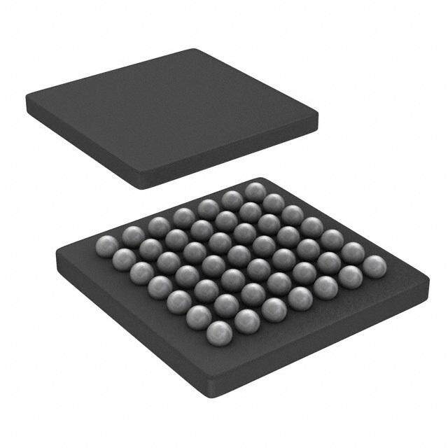
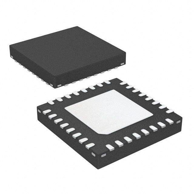
| 产品图片 |
|
| rohs | 符合RoHS无铅 / 符合限制有害物质指令(RoHS)规范要求 |
| 产品系列 | 嵌入式处理器和控制器,微控制器 - MCU,8位微控制器 -MCU,Silicon Labs C8051T605-GMC8051T60x |
| 数据手册 | |
| 产品型号 | C8051T605-GMC8051T605-GM |
| RAM容量 | 256 x 8 |
| 产品培训模块 | http://www.digikey.cn/PTM/IndividualPTM.page?site=cn&lang=zhs&ptm=25245 |
| 产品种类 | 8位微控制器 -MCU |
| 供应商器件封装 | 11-QFN(3x3) |
| 其它名称 | 336-1660-5 |
| 包装 | 管件 |
| 单位重量 | 24.090 mg |
| 可编程输入/输出端数量 | 8 |
| 商标 | Silicon Labs |
| 处理器系列 | C8051 |
| 外设 | POR,PWM,WDT |
| 安装风格 | SMD/SMT |
| 定时器数量 | 3 Timer |
| 封装 | Tube |
| 封装/外壳 | 10-VFDFN 裸露焊盘 |
| 封装/箱体 | QFN-11 |
| 工作温度 | -40°C ~ 85°C |
| 工作电源电压 | 1.8 V to 3.6 V |
| 工厂包装数量 | 122 |
| 振荡器类型 | 内部 |
| 接口类型 | I2C, SMBus, UART |
| 数据RAM大小 | 256 B |
| 数据Ram类型 | RAM |
| 数据总线宽度 | 8 bit |
| 数据转换器 | - |
| 最大工作温度 | + 85 C |
| 最大时钟频率 | 25 MHz |
| 最小工作温度 | - 40 C |
| 标准包装 | 122 |
| 核心 | 8051 |
| 核心处理器 | 8051 |
| 核心尺寸 | 8-位 |
| 片上ADC | Yes |
| 片上DAC | Without DAC |
| 电压-电源(Vcc/Vdd) | 1.8 V ~ 3.6 V |
| 电源电压-最大 | 3.6 V |
| 电源电压-最小 | 1.8 V |
| 程序存储器大小 | 2 kB |
| 程序存储器类型 | EPROMOTP |
| 程序存储容量 | 2KB(2K x 8) |
| 系列 | C8051T605 |
| 输入/输出端数量 | 8 I/O |
| 连接性 | SMBus(2 线/I²C), UART/USART |
| 速度 | 25MHz |
| 配用 | /product-detail/zh/C8051T600DK/336-1404-ND/1473874 |


- 商务部:美国ITC正式对集成电路等产品启动337调查
- 曝三星4nm工艺存在良率问题 高通将骁龙8 Gen1或转产台积电
- 太阳诱电将投资9.5亿元在常州建新厂生产MLCC 预计2023年完工
- 英特尔发布欧洲新工厂建设计划 深化IDM 2.0 战略
- 台积电先进制程称霸业界 有大客户加持明年业绩稳了
- 达到5530亿美元!SIA预计今年全球半导体销售额将创下新高
- 英特尔拟将自动驾驶子公司Mobileye上市 估值或超500亿美元
- 三星加码芯片和SET,合并消费电子和移动部门,撤换高东真等 CEO
- 三星电子宣布重大人事变动 还合并消费电子和移动部门
- 海关总署:前11个月进口集成电路产品价值2.52万亿元 增长14.8%


PDF Datasheet 数据手册内容提取
C8051T600/1/2/3/4/5/6 Mixed-Signal Byte-Programmable EPROM MCU Analog Peripherals H igh-Speed 8051μC Core s - 10-Bit ADC (‘T600/602/604 only) - Pipelined instruction architecture; executes 70% of • U p to 500ksps i nstructions in 1 or 2system clocks n • Up to 8 external inputs - U p to 25M IPS throughput with 25MHz clock • VREF external pin, Internal Regulator or VDD g • Internal or external start of conversion source - Expanded interrupt handler • Built-in temperature sensor Memory i - Comparator - 2 56 or 128Bytes internal data RAM s •• PCroongfrigaumrambaleb laes h iynsteterrreuspits o ar nrde sreets spoounrscee time - 8 , 4, 2, or 1.5kB byte-programmable EPeROM code • Low current memory On-Chip Debug Digital Peripherals D - C8051F300 can be used as code development - Up to 8 Port I/O with high sink current capability platform; complete development kit available - Hardware enhanced UART a nd SMBus™ serial - On-chip debug circuitry facilitates full speed, ports w non-intrusive in-system debug - Three general purpose 16-bit counter/timers - Provides breakpoints, single stepping, - 16-bit programmablee counter array (PCA) with three inspect/modify memory and registers capture/compare modules Supply V oltage 1.8 to 3.6V N • 8 or 16-bit PWM - On-chip LDO for internal core supply • Rising / falling edge capture - Built-in voltage supply monitor • Frequency output • Software timer T emperature Range: –40 to +85°C Clock Sourrces Package Options: - I nteronal oscillator: 24.5MHz with ±2% accuracy - 3 x 3 mm QFN11 supports crystal-less UART operation f - 2 x 2 mm QFN10 (C8051T606 Only) - External oscillator: RC, C, or CMOS Clock - MSOP10 (C8051T606 Only) d- Can switch between clock sources on-the-fly; useful - SOIC14 (C8051T600/1/2/3/4/5 Only) in power saving modes e d n e m m o c e R t o N Rev. 1.3 8/20 Copyright © 2020 by Silicon Laboratories C8051T600/1/2/3/4/5/6
C8051T600/1/2/3/4/5/6 Table of Contents 1. System Overview..................................................................................................... 13 s 2. Ordering Information............................................................................................... 16 n 3. Pin Definitions.......................................................................................................... 18 g 4. QFN-11 Package Specifications............................................................................. 23 5. SOIC-14 Package Specifications..........................................................................i.. 25 s 6. MSOP-10 Package Specifications.......................................................................... 27 e 7. QFN-10 Package Specifications............................................................................. 29 8. Electrical Characteristics.........................................................................D............... 31 8.1. Absolute Maximum Specifications..................................................................... 31 8.2. Electrical Characteristics................................................................................... 32 w 8.3. Typical Performance Curves............................................................................. 39 9. 10-Bit ADC (ADC0, C8051T600/2/4 only)...............................e................................. 41 9.1. Output Code Formatting.................................................................................... 42 N 9.2. 8-Bit Mode......................................................................................................... 42 9.3. Modes of Operation............................................. .............................................. 42 9.3.1. Starting a Conversion................................r................................................ 42 o 9.3.2. Tracking Modes......................................................................................... 43 9.3.3. Settling Time Requirements.............f......................................................... 44 9.4. Programmable Window Detector....................................................................... 48 d 9.4.1. Window Detector Example........................................................................ 50 e 9.5. ADC0 Analog Multiplexer (C8051T600/2/4 only)............................................... 51 10. Temperature Sensor (C8051T600d/2/4 only)......................................................... 53 10.1. Calibration....................................................................................................... 53 n 11. Voltage Reference Options................................................................................... 56 e 12. Voltage Regulator (REG0)..................................................................................... 58 13. Comparator0................m........................................................................................... 60 13.1. Comparator Multiplexer................................................................................... 64 14. CIP-51 Microcontmroller........................................................................................... 66 14.1. Instruction Set.................................................................................................. 67 14.1.1. Insotruction and CPU Timing.................................................................... 67 14.2. CIP-51 Register Descriptions.......................................................................... 72 c 15. Memory Organization............................................................................................ 75 e 15.1. Program Memory............................................................................................. 75 15.R2. Data Memory................................................................................................... 76 15.2.1. Internal RAM........................................................................................... 76 15.2.1.1. General Purpose Registers............................................................ 77 t o 15.2.1.2. Bit Addressable Locations.............................................................. 77 15.2.1.3. Stack ............................................................................................ 77 N 16. Special Function Registers................................................................................... 78 17. Interrupts................................................................................................................ 81 17.1. MCU Interrupt Sources and Vectors................................................................ 82 17.1.1. Interrupt Priorities.................................................................................... 82 17.1.2. Interrupt Latency..................................................................................... 82 2 Rev. 1.3
C8051T600/1/2/3/4/5/6 17.2. Interrupt Register Descriptions........................................................................ 83 17.3. INT0 and INT1 External Interrupt Sources...................................................... 88 s 18. Power Management Modes................................................................................... 90 n 18.1. Idle Mode......................................................................................................... 90 18.2. Stop Mode....................................................................................................... 91g 19. Reset Sources........................................................................................................ 93 i 19.1. Power-On Reset..........................................................................................s.... 94 19.2. Power-Fail Reset/VDD Monitor..............................................................e......... 95 19.3. External Reset................................................................................................. 95 D 19.4. Missing Clock Detector Reset......................................................................... 95 19.5. Comparator0 Reset......................................................................................... 95 19.6. PCA Watchdog Timer Reset..................................................w......................... 95 19.7. EPROM Error Reset........................................................................................ 96 e 19.8. Software Reset................................................................................................ 96 20. EPROM Memory...............................................................N...................................... 98 20.1. Programming and Reading the EPROM Memory...........................................98 20.1.1. EPROM Write Procedure........................................................................ 98 r 20.1.2. EPROM Read Procedure........................................................................ 99 o 20.2. Security Options.............................................................................................. 99 f 20.3. Program Memory CRC.................................................................................. 100 20.3.1. Performing 32-bit CRCs on Fuldl EPROM Content................................100 20.3.2. Performing 16-bit CRCs on 256-Byte EPROM Blocks..........................100 e 21. Oscillators and Clock Selection......................................................................... 101 d 21.1. System Clock Selection................................................................................. 101 21.2. Programmable Internal Hingh-Frequency (H-F) Oscillator..............................102 21.3. External Oscillator Drive Circuit..................................................................... 104 e 21.3.1. External RC Example............................................................................ 106 m 21.3.2. External Capacitor Example.................................................................. 106 22. Port Input/Output................................................................................................. 107 m 22.1. Port I/O Modes of Operation.......................................................................... 108 22.1.1. Port Pins Configured for Analog I/O...................................................... 108 o 22.1.2. Port Pins Configured For Digital I/O...................................................... 108 22.1.3.c Interfacing Port I/O to 5V Logic............................................................. 109 22.2. Assigning Port I/O Pins to Analog and Digital Functions...............................110 e 22.2.1. Assigning Port I/O Pins to Analog Functions........................................110 R 22.2.2. Assigning Port I/O Pins to Digital Functions..........................................110 22.2.3. Assigning Port I/O Pins to External Digital Event Capture Functions...111 t22.3. Priority Crossbar Decoder............................................................................. 112 o 22.4. Port I/O Initialization...................................................................................... 115 N 22.5. Special Function Registers for Accessing and Configuring Port I/O.............119 23. SMBus................................................................................................................... 121 23.1. Supporting Documents.................................................................................. 122 23.2. SMBus Configuration..................................................................................... 122 23.3. SMBus Operation.......................................................................................... 122 23.3.1. Transmitter Vs. Receiver....................................................................... 123 Rev. 1.3 3
C8051T600/1/2/3/4/5/6 23.3.2. Arbitration.............................................................................................. 123 23.3.3. Clock Low Extension............................................................................. 123 s 23.3.4. SCL Low Timeout.................................................................................. 123 n 23.3.5. SCL High (SMBus Free) Timeout......................................................... 124 23.4. Using the SMBus........................................................................................... 124g 23.4.1. SMBus Configuration Register.............................................................. 124 i 23.4.2. SMB0CN Control Register..................................................................s.. 128 23.4.3. Data Register.................................................................................e....... 131 23.5. SMBus Transfer Modes................................................................................. 132 D 23.5.1. Write Sequence (Master)...................................................................... 132 23.5.2. Read Sequence (Master)...................................................................... 133 23.5.3. Write Sequence (Slave).................................................w....................... 134 23.5.4. Read Sequence (Slave)........................................................................ 135 e 23.6. SMBus Status Decoding................................................................................ 135 24. UART0...............................................................................N.................................... 138 24.1. Enhanced Baud Rate Generation.................................................................. 139 24.2. Operational Modes........................................................................................ 140 r 24.2.1. 8-Bit UART............................................................................................ 140 o 24.2.2. 9-Bit UART............................................................................................ 141 f 24.3. Multiprocessor Communications................................................................... 142 25. Timers......................................................d............................................................. 146 25.1. Timer 0 and Timer 1...................................................................................... 148 e 25.1.1. Mode 0: 13-bit Counter/Timer............................................................... 148 d 25.1.2. Mode 1: 16-bit Counter/Timer............................................................... 149 25.1.3. Mode 2: 8-bit Countenr/Timer with Auto-Reload.....................................150 25.1.4. Mode 3: Two 8-bit Counter/Timers (Timer 0 Only)................................151 e 25.2. Timer 2.......................................................................................................... 156 m 25.2.1. 16-bit Timer with Auto-Reload............................................................... 156 25.2.2. 8-bit Timers with Auto-Reload............................................................... 157 m 26. Programmable Counter Array............................................................................. 161 26.1. PCA Counter/Timer....................................................................................... 162 o 26.2. PCA0 Interrupt Sources................................................................................. 163 26.3. Capcture/Compare Modules........................................................................... 164 26.3.1. Edge-triggered Capture Mode............................................................... 165 e 26.3.2. Software Timer (Compare) Mode.......................................................... 166 R 26.3.3. High-Speed Output Mode..................................................................... 167 26.3.4. Frequency Output Mode....................................................................... 168 t 26.3.5. 8-bit Pulse Width Modulator Mode....................................................... 169 o 26.3.6. 16-Bit Pulse Width Modulator Mode..................................................... 170 N 26.4. Watchdog Timer Mode.................................................................................. 171 26.4.1. Watchdog Timer Operation................................................................... 171 26.4.2. Watchdog Timer Usage........................................................................ 172 26.5. Register Descriptions for PCA0..................................................................... 174 27. C2 Interface.......................................................................................................... 179 27.1. C2 Interface Registers................................................................................... 179 4 Rev. 1.3
C8051T600/1/2/3/4/5/6 27.2. C2 Pin Sharing.............................................................................................. 186 Document Change List.............................................................................................. 187 s Contact Information................................................................................................... 189 n g i s e D w e N r o f d e d n e m m o c e R t o N Rev. 1.3 5
C8051T600/1/2/3/4/5/6 List of Figures 1. System Overview s F igure 1.1. C8051T600/2/4 Block Diagram ............................................................. 14 n F igure 1.2. C8051T601/3/5 Block Diagram ............................................................. 14 g F igure 1.3. C8051T606 Block Diagram ................................................................... 15 2. Ordering Information i s 3. Pin Definitions e F igure 3.1. C8051T600/1/2/3/4/5-GM QFN11 Pinout Diagram (Top View) .............20 F igure 3.2. C8051T600/1/2/3/4/5-GS SOIC14 Pinout Diagram (Top ViewD) ............20 F igure 3.3. C8051T606-GM QFN11 Pinout Diagram (Top View) ............................21 F igure 3.4. C8051T606-GT MSOP10 Pinout Diagram (Top View) ..........................21 w F igure 3.5. C8051T606-ZM QFN10 Pinout Diagram (Top View) ............................22 4. QFN-11 Package Specifications e F igure 4.1. QFN-11 Package Drawing .................................................................... 23 N F igure 4.2. QFN-11 PCB Land Pattern .................................................................... 24 5. SOIC-14 Package Specifications F igure 5.1. SOIC-14 Package Drawing ...................r................................................ 25 o F igure 5.2. SOIC-14 Recommended PCB Land Pattern .........................................26 6. MSOP-10 Package Specifications f F igure 6.1. MSOP-10 Package Drawing ................................................................. 27 d F igure 6.2. MSOP-10 PCB Land Pattern ................................................................. 28 e 7. QFN-10 Package Specifications F igure 7.1. QFN-10 Package Drawding .................................................................... 29 F igure 7.2. QFN-10 PCB Land Pattern .................................................................... 30 n 8. Electrical Characteristics e F igure 8.1. C8051T600/1/2/3/4/5 Normal Mode Supply Current vs. Frequency ( MPCE = 1) .............m........................................................................................... 39 F igure 8.2. C8051T606 Normal Mode Supply Current vs. Frequency (MPCE = 1) 39 F igure 8.3. C8051Tm600/1/2/3/4/5 Idle Mode Supply Current vs. Frequency ( MPCE = 1) ........................................................................................................ 40 F igure 8.4. C8o051T606 Idle Mode Digital Current vs. Frequency (MPCE = 1) .......40 9. 10-Bit ADC (ADC0, C8051T600/2/4 only) c F igure 9.1. ADC0 Functional Block Diagram ........................................................... 41 e F igure 9.2. 10-Bit ADC Track and Conversion Example Timing .............................43 F igRure 9.3. ADC0 Equivalent Input Circuits ............................................................. 44 F igure 9.4. ADC Window Compare Example: Right-Justified Data .........................50 F igure 9.5. ADC Window Compare Example: Left-Justified Data ...........................50 t o F igure 9.6. ADC0 Multiplexer Block Diagram .......................................................... 51 10. Temperature Sensor (C8051T600/2/4 only) N F igure 10.1. Temperature Sensor Transfer Function ..............................................53 F igure 10.2. T emperature Sensor Error with 1-Point Calibration at 0 °C ................54 11. Voltage Reference Options F igure 11.1. Voltage Reference Functional Block Diagram .....................................56 12. Voltage Regulator (REG0) 6 Rev. 1.3
C8051T600/1/2/3/4/5/6 13. Comparator0 F igure 13.1. Comparator0 Functional Block Diagram ............................................. 60 s F igure 13.2. Comparator Hysteresis Plot ................................................................ 61 n F igure 13.3. Comparator Input Multiplexer Block Diagram ......................................64 14. CIP-51 Microcontroller g F igure 14.1. CIP-51 Block Diagram ......................................................................... 66 i 15. Memory Organization s F igure 15.1. Program Memory Map ................................................................e......... 75 F igure 15.2. RAM Memory Map .............................................................................. 76 D 16. Special Function Registers 17. Interrupts 18. Power Management Modes w 19. Reset Sources e F igure 19.1. Reset Sources ..................................................................................... 93 F igure 19.2. Power-On and VDD Monitor Reset Timing ...N......................................94 20. EPROM Memory 21. Oscillators and Clock Selection r F igure 21.1. Oscillator Options .............................................................................. 101 o 22. Port Input/Output f F igure 22.1. Port I/O Functional Block Diagram .................................................... 107 F igure 22.2. Port I/O Cell Block Diagram .d............................................................. 108 F igure 22.3. Priority Crossbar Decoder Potential Pin Assignments ......................112 e F igure 22.4. Priority Crossbar Decoder Example 1 - No Skipped Pins .................113 d F igure 22.5. Priority Crossbar Decoder Example 2 - Skipping Pins ......................114 23. SMBus n F igure 23.1. SMBus Block Diagram ...................................................................... 121 e F igure 23.2. Typical SMBus Configuration ............................................................ 122 m F igure 23.3. SMBus Transaction ........................................................................... 123 F igure 23.4. Typical SMBus SCL Generation ........................................................ 125 m F igure 23.5. Typical Master Write Sequence ........................................................ 132 F igure 23.6. Typical Master Read Sequence ........................................................ 133 o F igure 23.7. Typical Slave Write Sequence .......................................................... 134 F igure 23.c8. Typical Slave Read Sequence .......................................................... 135 24. UART0 e F igure 24.1. UART0 Block Diagram ...................................................................... 138 R F igure 24.2. UART0 Baud Rate Logic ................................................................... 139 F igure 24.3. UART Interconnect Diagram ............................................................. 140 tF igure 24.4. 8-Bit UART Timing Diagram .............................................................. 140 o F igure 24.5. 9-Bit UART Timing Diagram .............................................................. 141 N F igure 24.6. UART Multi-Processor Mode Interconnect Diagram .........................142 25. Timers F igure 25.1. T0 Mode 0 Block Diagram ................................................................. 149 F igure 25.2. T0 Mode 2 Block Diagram ................................................................. 150 F igure 25.3. T0 Mode 3 Block Diagram ................................................................. 151 F igure 25.4. Timer 2 16-Bit Mode Block Diagram .................................................156 Rev. 1.3 7
C8051T600/1/2/3/4/5/6 F igure 25.5. Timer 2 8-Bit Mode Block Diagram ................................................... 157 26. Programmable Counter Array s F igure 26.1. PCA Block Diagram ........................................................................... 161 n F igure 26.2. PCA Counter/Timer Block Diagram ................................................... 162 F igure 26.3. PCA Interrupt Block Diagram ............................................................ 163g F igure 26.4. PCA Capture Mode Diagram ............................................................. 165 i F igure 26.5. PCA Software Timer Mode Diagram ...............................................s..166 F igure 26.6. PCA High-Speed Output Mode Diagram ....................................e.......167 F igure 26.7. PCA Frequency Output Mode ........................................................... 168 D F igure 26.8. PCA 8-Bit PWM Mode Diagram ........................................................ 169 F igure 26.9. PCA 16-Bit PWM Mode ..................................................................... 170 F igure 26.10. PCA Module 2 with Watchdog Timer Enabled .........w.......................171 27. C2 Interface e F igure 27.1. Typical C2 Pin Sharing ...................................................................... 186 N r o f d e d n e m m o c e R t o N 8 Rev. 1.3
C8051T600/1/2/3/4/5/6 List of Tables 1. System Overview s 2. Ordering Information n T able 2.1. Product Selection Guide ......................................................................... 16 g T able 2.2. Product Selection Guide (These OPNs are Obsolete) ...........................17 3. Pin Definitions i s T able 3.1. Pin Definitions for the C8051T600/1/2/3/4/5 ...........................................18 e T able 3.2. Pin Definitions for the C8051T606 .......................................................... 19 4. QFN-11 Package Specifications D T able 4.1. QFN-11 Package Dimensions ................................................................ 23 T able 4.2. QFN-11 PCB Land Pattern Dimensions ................................................. 24 w 5. SOIC-14 Package Specifications T able 5.1. SOIC-14 Package Dimensions ..............................e................................. 25 T able 5.2. SOIC-14 PCB Land Pattern Dimensions ................................................ 26 N 6. MSOP-10 Package Specifications T able 6.1. MSOP-10 Package Dimensions ............... .............................................. 27 T able 6.2. MSOP-10 PCB Land Pattern Dimensionsr ..............................................28 o 7. QFN-10 Package Specifications T able 7.1. QFN-10 Package Dimensions .......f......................................................... 29 T able 7.2. QFN-10 PCB Land Pattern Dimensions ................................................. 30 d 8. Electrical Characteristics e T able 8.1. Absolute Maximum Ratings .................................................................... 31 T able 8.2. Global Electrical Characdteristics ............................................................. 32 T able 8.3. Port I/O DC Electrical Characteristics ..................................................... 34 n T able 8.4. Reset Electrical Characteristics .............................................................. 35 e T able 8.5. Internal Voltage Regulator Electrical Characteristics .............................35 T able 8.6. EPROM Elecmtrical Characteristics .......................................................... 35 T able 8.7. Internal High-Frequency Oscillator Electrical Characteristics .................36 T able 8.8. Temperamture Sensor Electrical Characteristics ......................................36 T able 8.9. Voltage Reference Electrical Characteristics .........................................36 T able 8.10. AoDC0 Electrical Characteristics ............................................................ 37 T able 8.11. Comparator Electrical Characteristics .................................................. 38 c 9. 10-Bit ADC (ADC0, C8051T600/2/4 only) e 10. Temperature Sensor (C8051T600/2/4 only) 11. VoRltage Reference Options 12. Voltage Regulator (REG0) 13 . Comparator0 t o14. CIP-51 Microcontroller T able 14.1. CIP-51 Instruction Set Summary .......................................................... 68 N 15. Memory Organization 16. Special Function Registers T able 16.1. Special Function Register (SFR) Memory Map ....................................78 T able 16.2. Special Function Registers ................................................................... 78 17. Interrupts Rev. 1.3 9
C8051T600/1/2/3/4/5/6 T able 17.1. Interrupt Summary ................................................................................ 83 18. Power Management Modes s 19. Reset Sources n 20. EPROM Memory T able 20.1. Security Byte Decoding ........................................................................ 99g 21. Oscillators and Clock Selection i 22. Port Input/Output s T able 22.1. Port I/O Assignment for Analog Functions ..................................e.......110 T able 22.2. Port I/O Assignment for Digital Functions ...........................................110 D T able 22.3. Port I/O Assignment for External Digital Event Capture Functions ....111 23. SMBus T able 23.1. SMBus Clock Source Selection ...................................w....................... 125 T able 23.2. Minimum SDA Setup and Hold Times ................................................126 e T able 23.3. Sources for Hardware Changes to SMB0CN .....................................130 T able 23.4. SMBus Status Decoding .................................N.................................... 136 24. UART0 T able 24.1. Timer Settings for Standard Baud Rates r U sing The Internal 24.5 MHz Oscillator ..............................................145 o T able 24.2. Timer Settings for Standard Baud Rates f U sing an External 22.1184 MHz Oscillator .........................................145 25. Timers d 26. Programmable Counter Array e T able 26.1. PCA Timebase Input Options ............................................................. 162 d T able 26.2. PCA0CPM Bit Settings for PCA Capture/Compare Modules .............164 T able 26.3. Watchdog Timer Timneout Intervals1 ................................................... 173 27. C2 Interface e m m o c e R t o N 10 Rev. 1.3
C8051T600/1/2/3/4/5/6 List of Registers S FR Definition 9.1. ADC0CF: ADC0 Configuration ...................................................... 45 s S FR Definition 9.2. ADC0H: ADC0 Data Word MSB .................................................... 46 n S FR Definition 9.3. ADC0L: ADC0 Data Word LSB ...................................................... 46 g S FR Definition 9.4. ADC0CN: ADC0 Control ................................................................ 47 S FR Definition 9.5. ADC0GTH: ADC0 Greater-Than Data High Byte ........................i..48 s S FR Definition 9.6. ADC0GTL: ADC0 Greater-Than Data Low Byte ............................48 e S FR Definition 9.7. ADC0LTH: ADC0 Less-Than Data High Byte ................................49 S FR Definition 9.8. ADC0LTL: ADC0 Less-Than Data Low Byte ..................D...............49 S FR Definition 9.9. AMX0SL: AMUX0 Positive Channel Select ...................................52 S FR Definition 10.1. TOFFH: Temperature Offset Measurement High Byte ................55 w S FR Definition 10.2. TOFFL: Temperature Offset Measurement Low Byte .................55 S FR Definition 11.1. REF0CN: Reference Control ......................e................................. 57 S FR Definition 12.1. REG0CN: Voltage Regulator Control ..........................................59 N S FR Definition 13.1. CPT0CN: Comparator0 Control ................................................... 62 S FR Definition 13.2. CPT0MD: Comparator0 Mode Selec tion .....................................63 S FR Definition 13.3. CPT0MX: Comparator0 MUX Selerction ......................................65 o S FR Definition 14.1. DPL: Data Pointer Low Byte ........................................................ 72 S FR Definition 14.2. DPH: Data Pointer High Bytef ....................................................... 72 S FR Definition 14.3. SP: Stack Pointer ......................................................................... 73 d S FR Definition 14.4. ACC: Accumulator ....................................................................... 73 e S FR Definition 14.5. B: B Register ................................................................................ 73 S FR Definition 14.6. PSW: Program Sdtatus Word ........................................................ 74 S FR Definition 17.1. IE: Interrupt Enable ...................................................................... 84 n S FR Definition 17.2. IP: Interrupt Priority ...................................................................... 85 e S FR Definition 17.3. EIE1: Extended Interrupt Enable 1 ..............................................86 S FR Definition 17.4. EIP1: Emxtended Interrupt Priority 1 ..............................................87 S FR Definition 17.5. IT01CF: INT0/INT1 Configuration ................................................ 89 S FR Definition 18.1. PmCON: Power Control .................................................................. 92 S FR Definition 19.1. RSTSRC: Reset Source .............................................................. 97 S FR Definition 21o.1. OSCICL: Internal H-F Oscillator Calibration ..............................102 S FR Definition 21.2. OSCICN: Internal H-F Oscillator Control ...................................103 c S FR Definition 21.3. OSCXCN: External Oscillator Control ........................................105 e S FR Definition 22.1. XBR0: Port I/O Crossbar Register 0 ..........................................116 S FR DRefinition 22.2. XBR1: Port I/O Crossbar Register 1 ..........................................117 S FR Definition 22.3. XBR2: Port I/O Crossbar Register 2 ..........................................118 S F R Definition 22.4. P0: Port 0 ................................................................................... 119 t oS FR Definition 22.5. P0MDIN: Port 0 Input Mode ....................................................... 120 S FR Definition 22.6. P0MDOUT: Port 0 Output Mode ................................................120 N S FR Definition 23.1. SMB0CF: SMBus Clock/Configuration ......................................127 S FR Definition 23.2. SMB0CN: SMBus Control .......................................................... 129 S FR Definition 23.3. SMB0DAT: SMBus Data ............................................................ 131 S FR Definition 24.1. SCON0: Serial Port 0 Control .................................................... 143 S FR Definition 24.2. SBUF0: Serial (UART0) Port Data Buffer ..................................144 Rev. 1.3 11
C8051T600/1/2/3/4/5/6 S FR Definition 25.1. CKCON: Clock Control .............................................................. 147 S FR Definition 25.2. TCON: Timer Control ................................................................. 152 s S FR Definition 25.3. TMOD: Timer Mode ................................................................... 153 n S FR Definition 25.4. TL0: Timer 0 Low Byte ............................................................... 154 S FR Definition 25.5. TL1: Timer 1 Low Byte ............................................................... 154g S FR Definition 25.6. TH0: Timer 0 High Byte ............................................................. 155 i S FR Definition 25.7. TH1: Timer 1 High Byte ...........................................................s.. 155 S FR Definition 25.8. TMR2CN: Timer 2 Control ..................................................e....... 158 S FR Definition 25.9. TMR2RLL: Timer 2 Reload Register Low Byte ..........................159 D S FR Definition 25.10. TMR2RLH: Timer 2 Reload Register High Byte ......................159 S FR Definition 25.11. TMR2L: Timer 2 Low Byte ....................................................... 159 S FR Definition 25.12. TMR2H Timer 2 High Byte ................................w....................... 160 S FR Definition 26.1. PCA0CN: PCA Control .............................................................. 174 e S FR Definition 26.2. PCA0MD: PCA Mode ................................................................ 175 S FR Definition 26.3. PCA0CPMn: PCA Capture/Compare MoNde ..............................176 S FR Definition 26.4. PCA0L: PCA Counter/Timer Low Byte ......................................177 S FR Definition 26.5. PCA0H: PCA Counter/Timer High Byte .....................................177 r S FR Definition 26.6. PCA0CPLn: PCA Capture Module Low Byte .............................178 o S FR Definition 26.7. PCA0CPHn: PCA Capture Module High Byte ...........................178 f C 2 Register Definition 27.1. C2ADD: C2 Address ...................................................... 179 C 2 Register Definition 27.2. DEVICEID: C2 Ddevice ID ...............................................180 C 2 Register Definition 27.3. REVID: C2 Revision ID .................................................. 180 e C 2 Register Definition 27.4. DEVCTL: C2 Device Control ..........................................181 d C 2 Register Definition 27.5. EPCTL: EPROM Programming Control Register ...........181 C 2 Register Definition 27.6. EPDATn: C2 EPROM Data ..............................................182 C 2 Register Definition 27.7. EPSTAT: C2 EPROM Status .........................................182 e C 2 Register Definition 27.8. EPADDRH: C2 EPROM Address High Byte ..................183 m C 2 Register Definition 27.9. EPADDRL: C2 EPROM Address Low Byte ...................183 C 2 Register Definition 27.10. CRC0: CRC Byte 0 ...................................................... 184 m C 2 Register Definition 27.11. CRC1: CRC Byte 1 ...................................................... 184 C 2 Register Definition 27.12. CRC2: CRC Byte 2 ...................................................... 185 o C 2 Register Definition 27.13. CRC3: CRC Byte 3 ...................................................... 185 c e R t o N 12 Rev. 1.3
C8051T600/1/2/3/4/5/6 1. System Overview s C8051T600/1/2/3/4/5/6 devices are fully integrated, mixed-signal, system-on-a-chip MCUs. Highlighted features are listed below. Refer to Ta ble2.1 for specific product feature selection and part ordering num- n bers. g H igh-speed pipelined 8051-compatible microcontroller core (up to 25MIPS) i In-system, full-speed, non-intrusive debug interface (on-chip) s C8051F300 ISP Flash device is available for quick in-system code development e 1 0-bit 500ksps Single-ended ADC with analog multiplexer and integrated temperature sensor P recision calibrated 24.5MHz internal oscillator D 8 k, 4 k, 2k or 1.5 kB of on-chip Byte-Programmable EPROM—(512 bytes are reserved on 8k version) 256 or 128 bytes of on-chip RAM w SMBus/I2C, and ART serial interfaces implemented in hardware Three general-purpose 16-bit timers e Programmable Counter/Timer Array (PCA) with three capture/compare modules and Watchdog Timer function On-chip Power-On Reset and Supply Monitor N On-chip Voltage Comparator 8 or 6 Port I/O r o With on-chip power-on reset, V monitor, watchdog timer, and clock oscillator, the C8051T600/1/2/3/4/5/6 DD f devices are truly stand-alone, system-on-a-chip solutio ns. User software has complete control of all peripherals and may individually shut down any or all pderipherals for power savings. e Code written for the C8051T600/1/2/3/4/5/6 family of processors will run on the C8051F300 Mixed-Signal ISP Flash microcontroller, providing a quick, cdost-effective way to develop code without requiring special emulator circuitry. The C8051T600/1/2/3/4/5/6 processors include Silicon Laboratories’ 2-Wire C2 Debug n and Programming interface, which allows non-intrusive (uses no on-chip resources), full speed, in-circuit debugging using the production MCUe installed in the final application. This debug logic supports inspection of memory, viewing and modification of special function registers, setting breakpoints, single stepping, and run and halt commands. All analmog and digital peripherals are fully functional while debugging using C2. The two C2 interface pins can be shared with user functions, allowing in-system debugging without occu- pying package pins. m Each device is specified for 1.8–3.6 V operation over the industrial temperature range (–45 to + 85°C). An o internal LDO is used to supply the processor core voltage at 1 .8V. The Port I/O and RST pins are tolerant of input signals cup to 5 V. See T able2.1 for ordering information. Block diagrams of the devices in the C 8051T600/1/2/3/4/5/6 family are shown in Figure 1.1, Figure 1.2, and Figure1.3. e R t o N Rev. 1.3 13
C8051T600/1/2/3/4/5/6 s n g i s e D w e N r F igure 1.1. C8051T600/2/4 Block Diagram o f d e d n e m m o c e R F igure 1.2. C8051T601/3/5 Block Diagram t o N 14 Rev. 1.3
C8051T600/1/2/3/4/5/6 s n g i s e D w e N r F igure 1.3. C8051T606 Block Diagram o f d e d n e m m o c e R t o N Rev. 1.3 15
C8051T600/1/2/3/4/5/6 2. Ordering Information s T able 2.1. Product Selection Guide n cillator er Array 2mpliant) sig ) Os nt r s o Part Number MIPS (Peak) OTP EPROM (Bytes RAM (Bytes) Calibrated Internal 2SMBus/IC UART Timers (16-bit) Programmable Cou Digital Port I/Os 10-bit 500ksps ADC Temperature SensoeAnalog Comparator wLead-Free (ROHS C DPackagee C8051T600-GM 25 8k1 256 Y Y Y 3 Y 8 Y NY 1 Y QFN-11 C8051T600-GS 25 8k1 256 Y Y Y 3 Y 8 Y Y 1 Y SOIC-14 r C8051T604-GS 25 2k 256 Y Y Y 3 Yo8 Y Y 1 Y SOIC-14 C8051T605-GM 25 2k 256 Y Y Y 3fY 8 — — 1 Y QFN-11 C8051T605-GS 25 2k 256 Y Y Yd3 Y 8 — — 1 Y SOIC-14 e Notes: 1. 512 Bytes Reserved d 2. Lead Finish is 100% Matte Tin (Sn) n e m m o c e R t o N 16 Rev. 1.3
C8051T600/1/2/3/4/5/6 T able 2.2. Product Selection Guide (These OPNs are Obsolete) s n cillator er Array 2mpliant) ig ) Os nt r s o s Part Number MIPS (Peak) OTP EPROM (Bytes RAM (Bytes) Calibrated Internal 2SMBus/IC UARTeTimers (16-bit)tProgrammable CoueDigital Port I/Os 10-bit 500ksps ADC Temperature SensoeAnalog Comparator wLead-Free (ROHS C DPackagee C8051T601-GM 25 8k1 256 Y Y Y 3 Y 8 — — 1 Y QFN-11 l N C8051T601-GS 25 8k1 256 Y oY Y 3 Y 8 — — 1 Y SOIC-14 C8051T602-GM 25 4k 256sY Y Y 3 Y r8 Y Y 1 Y QFN-11 o C8051T602-GS 25 4k 256 Y Y Y 3 Y 8 Y Y 1 Y SOIC-14 b f C8051T603-GM 25 4k 256 Y Y Y 3 Y 8 — — 1 Y QFN-11 d O C8051T603-GS 25 4k 256 Y Y Y 3 Y 8 — — 1 Y SOIC-14 e C8051T604-GM 25 2k 256 Y Y Y 3 Y 8 Y Y 1 Y QFN-11 d C8051T606-GM 25 1.5k 128 Y Y Y 3 Y 6 — — 1 Y QFN-11 n C8051T606-GT 25 1.5k e128 Y Y Y 3 Y 6 — — 1 Y MSOP-10 C8051T606-ZM 25 1.5mk 128 Y Y Y 3 Y 6 — — 1 Y QFN-10 Notes: m 1. 512 Bytes Reserved 2. Lead Finish is 100% Matte Tin (Sn) o c e R t o N Rev. 1.3 17
C8051T600/1/2/3/4/5/6 3. Pin Definitions s n T able 3.1. P in Definitions for the C8051T600/1/2/3/4/5 g Name QFN11 SOIC14 Type Description i Pin Pin s e V 3 7 Power Supply Voltage. DD D GND 11 3 Ground. RST / 8 14 D I/O Device Reset. Open-drain output of internal P OR or V monitor. DD w e C2CK D I/O Clock signal for the C2 Debug Interface. N P0.7 / 10 2 D I/O or Port 0.7. A In r C2D D I/O Bi-directional data signoal for the C2 Debug Interface. P0.0 / 1 5 D I/O or Port 0.0. f A In d VREF A In External VeREF input. d P0.1 2 6 D I/O or Port 0.1. A In n P0.2 / 4 8 D I/O oer Port 0.2. A In m V A In V Programming Supply Voltage. PP PP m P0.3 / 5 10 D I/O or Port 0.3. A In o EXTCLK c A I/O or External Clock Pin. This pin can be used as the external clock e D In input for CMOS, capacitor, or RC oscillator configurations. P0.4R 6 12 D I/O or Port 0.4. A In tP0.5 7 13 D I/O or Port 0.5. o A In N P0.6 / 9 1 D I/O or Port 0.6. A In CNVSTR D In ADC0 External Convert Start Input. NC — 4,9,11 No Connection. 18 Rev. 1.3
C8051T600/1/2/3/4/5/6 T able 3.2. P in Definitions for the C8051T606 s n Name QFN11 MSOP10 QFN10 Type Description Pin Pin Pin g V 3 3 2 Power Supply Voltage. i DD s GND 9 9 8 Ground (Required). e GND* 11 — — Ground (Optional). D RST / 8 8 7 D I/O Device Reset. Open-drain output of internal POR or VDD monitor. w C2CK D I/O Clock signal for the C2 Debeug Interface. P0.7 / 10 10 9 D I/O or Port 0.7. N A In r C2D D I/O Bi-directional data signal for the C2 Debug Interface. o P0.1 2 2 1 D I/O or Port 0.1. f A In d P0.2 / 4 4 3 D I/O or Port 0.2. e A In d V A In V Programming Supply Voltage. PP PP n P0.3 / 5 5 4 D I/O or Port 0.3. e A In m EXTCLK A I/O or External Clock Pin. This pin can be used as the exter- m D In nal clock input for CMOS, capacitor, or RC oscillator configurations. P0.4 6 o 6 5 D I/O or Port 0.4. A In c P0.5 e7 7 6 D I/O or Port 0.5. A In R NC 1 1 10 No Connection. t o N Rev. 1.3 19
C8051T600/1/2/3/4/5/6 s n g i s e D w e N r o F igure 3.1. C8051T600/1/2/3/4/5-GM QFN11 Pinout Diagram (Top View) f d e d n e m m o c e R t o N F igure 3.2. C8051T600/1/2/3/4/5-GS SOIC14 Pinout Diagram (Top View) 20 Rev. 1.3
C8051T600/1/2/3/4/5/6 s n g i s e D w e N r o F igure 3.3. C8051T606-GM QFN11 Pfinout Diagram (Top View) d e d n e m m o c eF igure 3.4. C8051T606-GT MSOP10 Pinout Diagram (Top View) R t o N Rev. 1.3 21
C8051T600/1/2/3/4/5/6 s n g i s e D w e N r F igure 3.5. C8051T606-ZM QFN10 Pinoout Diagram (Top View) f d e d n e m m o c e R t o N 22 Rev. 1.3
C8051T600/1/2/3/4/5/6 4. QFN-11 Package Specifications s n g i s e D w e N r o F igure 4.1. QFN-11 Pacfkage Drawing d T able 4.1. QFN-11 Package Dimensions e Dimension Min Nom Mdax Dimension Min Nom Max A 0.80 0.90 1.00 E 3.00 BSC n A1 0.03 0.07 0.11 E2 2.20 2.25 2.30 e A3 0.25 REF L 0.45 0.55 0.65 b 0.18 m0.25 0.30 aaa — — 0.15 D 3.00 BSC bbb — — 0.15 D2 1.30m 1.35 1.40 ddd — — 0.05 e 0.50 BSC eee — — 0.08 Notes: o 1. All dimensions shown are in millimeters (mm) unless otherwise noted. c 2. Dimensioning and Tolerancing per ANSI Y14.5M-1994. 3. eThis drawing conforms to the JEDEC Solid State Outline MO-243, variation VEED except for custom features D2, E2, and L which are toleranced per supplier designation. R4. Recommended card reflow profile is per the JEDEC/IPC J-STD-020 specification for Small Body Components. t o N Rev. 1.3 23
C8051T600/1/2/3/4/5/6 s n g i s e D w e N r F igure 4.2. QFN-11 PCB Laond Pattern f T able 4.2. QFN-11 PCB Land Pattern Dimensions d Dimension Min Max e Dimension Min Max C1 2.75 2.85d X2 1.40 1.50 C2 2.75 2.85 Y1 0.65 0.75 n E 0.50 BSC Y2 2.30 2.40 X1 0.20 e 0.30 Notes: m General 1. All dimensions shown are in millimeters (mm) unless otherwise noted. m 2. This Land Pattern Design is based on the IPC-7351 guidelines. Solder Mask Doesign 3. All metal pads are to be non-solder mask defined (NSMD). Clearance between the solder m cask and the metal pad is to be 60m minimum, all the way around the pad. e Stencil Design R 4. A stainless steel, laser-cut and electro-polished stencil with trapezoidal walls should be used to assure good solder paste release. 5. T he stencil thickness should be 0.125mm (5 mils). 6. The ratio of stencil aperture to land pad size should be 1:1 for all perimeter pins. t o 7. A 3 x 1 array of 1.30x 0.60 mm openings on 0.80mm pitch should be used for the center pad. N Card Assembly 8. A No-Clean, Type-3 solder paste is recommended. 9. The recommended card reflow profile is per the JEDEC/IPC J-STD-020 specification for Small Body Components. 24 Rev. 1.3
C8051T600/1/2/3/4/5/6 5. SOIC-14 Package Specifications s n g i s e D w e N r o f d e F igure 5.1. SOIC-14 Package Drawing d n T able 5.1. SOIC-14 Package Dimensions e Dimension Min Nom Max Dimension Min Nom Max m A — — 1.75 L 0.40 — 1.27 A1 0.10 — 0.25 L2 0.25 BSC m b 0.33 — 0.51 0° — 8° c 0.17 — 0.25 aaa 0.10 o D 8.65 BSC bbb 0.20 E c 6.00 BSC ccc 0.10 Ee1 3.90 BSC ddd 0.25 e 1.27 BSC R Notes: 1. All dimensions shown are in millimeters (mm). t 2. Dimensioning and Tolerancing per ANSI Y14.5M-1994. o 3. This drawing conforms to JEDEC outline MS012, variation AB. 4. Recommended card reflow profile is per the JEDEC/IPC J-STD-020 specification for Small Body N Components. Rev. 1.3 25
C8051T600/1/2/3/4/5/6 s n g i s e D w e N r o F igure 5.2. SOIC-14 Recommenfded PCB Land Pattern d T able 5.2. SOIC-14 PCB Land Pattern Dimensions e Dimension Min Maxd Dimension Min Max C1 5.30 5.40 X1 0.50 0.60 n E 1.27 BSC Y1 1.45 1.55 e Notes: General m 1. All dimensions shown are in millimeters (mm) unless otherwise noted. 2. This Land Pattern Design is based on the IPC-7351 guidelines. m Solder Mask Design 3. All metoal pads are to be non-solder mask defined (NSMD). Clearance between the solder m ask and the metal pad is to be 60m minimum, all the way around the pad. c Stencil Design e 4. A stainless steel, laser-cut and electro-polished stencil with trapezoidal walls should be used R to assure good solder paste release. 5. T he stencil thickness should be 0.125mm (5 mils). 6. The ratio of stencil aperture to land pad size should be 1:1 for all perimeter pads. t o Card Assembly 7. A No-Clean, Type-3 solder paste is recommended. N 8. The recommended card reflow profile is per the JEDEC/IPC J-STD-020 specification for Small Body Components. 26 Rev. 1.3
C8051T600/1/2/3/4/5/6 6. MSOP-10 Package Specifications s n g i s e D w e N r o f d e d n F iguree 6.1. MSOP-10 Package Drawing m T able 6.1. MSOP-10 Package Dimensions m Dimension Min Nom Max Dimension Min Nom Max A — — 1.10 e 0.50 BSC o A1 0.00 — 0.15 L 0.40 0.60 0.80 c A2 0.75 0.85 0.95 L2 0.25 BSC eb 0.17 — 0.33 0° — 8° R c 0.08 — 0.23 aaa — — 0.20 D 3.00 BSC bbb — — 0.25 E 4.90 BSC ccc — — 0.10 t E1 3.00 BSC ddd — — 0.08 o Notes: N 1. All dimensions shown are in millimeters (mm). 2. Dimensioning and Tolerancing per ANSI Y14.5M-1994. 3. This drawing conforms to JEDEC outline MO-187, Variation “BA”. 4. Recommended card reflow profile is per the JEDEC/IPC J-STD-020 specification for Small Body Components. Rev. 1.3 27
C8051T600/1/2/3/4/5/6 s n g i s e D w e N F igure 6.2. MSOP-10 PCB Lanrd Pattern o f T able 6.2. MSOP-10 PCB Land Pattern Dimensions d Dimension Min Max Dimension Min Max e C1 4.40 REF X1 — 0.30 E 0.50 BSC d Y1 1.40 REF G1 3.00 — Z1 — 5.80 n Notes: e General 1. All dimensions shown are in millimeters (mm) unless otherwise noted. m 2. Dimensioning and Tolerancing per ASME Y14.5M-1994. 3. This Land Pattern Design is based on the IPC-7351 guidelines. 4. All dimensionms shown are at Maximum Material Condition (MMC). Least Material Condition (LMC) is calculated based on a Fabrication A llowance of 0.05mm. o Solder Mask Design 5. All metal pads are to be non-solder mask defined (NSMD). Clearance between the solder c m ask and the metal pad is to be 60m minimum, all the way around the pad. e Stencil Design R 6. A stainless steel, laser-cut and electro-polished stencil with trapezoidal walls should be used to assure good solder paste release. 7. T he stencil thickness should be 0.125mm (5 mils). t 8. The ratio of stencil aperture to land pad size should be 1:1 for all perimeter pads. o N Card Assembly 9. A No-Clean, Type-3 solder paste is recommended. 10. The recommended card reflow profile is per the JEDEC/IPC J-STD-020 specification for Small Body Components. 28 Rev. 1.3
C8051T600/1/2/3/4/5/6 7. QFN-10 Package Specifications s n g i s e D w e N r o f d e d n e m F igure 7.1. QFN-10 Package Drawing m T able 7.1. QFN-10 Package Dimensions o Dimension Min Nom Max Dimension Min Nom Max c A 0.70 0.75 0.80 L 0.55 0.60 0.65 e A1 0.00 — 0.05 L1 — — 0.15 R b 0.18 0.25 0.30 aaa — — 0.10 D 2.00 BSC. bbb — — 0.10 t e 0.50 BSC. ccc — — 0.05 o E 2.00 BSC. ddd — — 0.08 N Notes: 1. All dimensions shown are in millimeters (mm) unless otherwise noted. 2. Dimensioning and Tolerancing per ANSI Y14.5M-1994. 3. This drawing conforms to JEDEC outline MO-220, variation WCCD-5 except for feature L which is toleranced per supplier designation. 4. Recommended card reflow profile is per the JEDEC/IPC J-STD-020 specification for Small Body Components. Rev. 1.3 29
C8051T600/1/2/3/4/5/6 s n g i s e D w e N r o F igure 7.2. QFN-10 PCBf Land Pattern d T able 7.2. QFN-10 PCBe Land Pattern Dimensions Dimension Min Maxd Dimension Min Max e 0.50 BSCn. X1 0.20 0.30 C1 1.70 1.80 Y1 0.85 0.95 e C2 1.70 1.80 m Notes: General 1. All dimensionms shown are in millimeters (mm) unless otherwise noted. 2. Dimensioning and Tolerancing is per the ANSI Y14.5M-1994 specification. 3. This Land Pattern Design is based on IPC-SM-782 guidelines. 4. All dimoensions shown are at Maximum Material Condition (MMC). Least Material Condition (LMC) is calculated based on a Fabrication Allowance of 0.05mm. c Soldeer Mask Design 5. All metal pads are to be non-solder mask defined (NSMD). Clearance between the solder R m ask and the metal pad is to be 60m minimum, all the way around the pad. Stencil Design t 6. A stainless steel, laser-cut and electro-polished stencil with trapezoidal walls should be used o to assure good solder paste release. 7. T he stencil thickness should be 0.125mm (5 mils). N 8. The ratio of stencil aperture to land pad size should be 1:1 for the perimeter pads. Card Assembly 9. A No-Clean, Type-3 solder paste is recommended. 10. The recommended card reflow profile is per the JEDEC/IPC J-STD-020 specification for Small Body Components. 30 Rev. 1.3
C8051T600/1/2/3/4/5/6 8. Electrical Characteristics s 8.1. Absolute Maximum Specifications T able 8.1. Absolute Maximum Ratings n g Parameter Conditions Min Typ Max Units i s Ambient temperature under bias –55 — 125 °C e Storage temperature –65 — 150 °C D Voltage on RST or any Port I/O pin V > 2.2V –0.3 — 5.8 V DD (except VPP during programming) with VDD < 2.2V –0.3 — VD D+ 3.6 V respect to GND w Voltage on VPP with respect to GND VDD > 2.4 V –0.3 e — 7.0 V during a programming operation N Duration of High-voltage on V pin V > (V + 3.6V) — — 10 s PP PP DD (cumulative) r Voltage on V with respect to GND Regulator in Normal Mode –0.3 — 4.2 V DD o Regulator in Bypass Mode –0.3 — 1.98 V f Maximum total current through V or — — 500 mA DD GND d e Maximum output current sunk or — — 100 mA sourced by RST or any Port pin d Note: Stresses above those listed under “Absnolute Maximum Ratings” may cause permanent damage to the device. This is a stress rating only and functional operation of the devices at those or any other conditions above those indicated in the operation lisetings of this specification is not implied. Exposure to maximum rating conditions for extended periods may affect device reliability. m m o c e R t o N Rev. 1.3 31
C8051T600/1/2/3/4/5/6 8.2. Electrical Characteristics s T able 8.2. Global Electrical Characteristics – 40 to +85 °C, 25MHz system clock unless otherwise specified. n g Parameter Conditions Min Typ Max Units i Supply Vo ltage (Note1) Regulator in Normal Mode 1.8 3.0 3.6 sV Regulator in Bypass Mode 1.7 1.8 1.9 V e C8051T600/1/2/3/4/5 Digital Sup- VD D= 1.8V , Clock = 25MHz — 4.3 D6.0 mA ply Current with CPU Active V = 1.8V , Clock = 1MHz — 2.0 — mA D D VD D= 3.0V , Clock = 25MHz — 5 .0 6.0 mA VD D= 3.0V , Clock = 1MHz — w2.4 — mA C8051T600/1/2/3/4/5 Digital Sup- VD D= 1.8V , Clock = 25MHz —e 1.7 2.5 mA ply Current with CPU Inactive (not V = 1.8V , Clock = 1MHz — 0.5 — mA D D N accessing EPROM) V = 3.0V , Clock = 25MHz — 1.8 2.6 mA D D VD D= 3.0V , Clock = 1MHz — 0.6 — mA r C8051T600/1/2/3/4/5 Digital Sup- Oscillator not running (stop mode), — 1 — μA o ply Current (shutdown) Internal Regulator Off f Oscillator not runnin g (stop or sus- — 450 — μA pend mode), Interdnal Regulator On C8051T606 Digital Supply Current V = 1.8V , eClock = 25MHz — 4.6 6.0 mA D D with CPU Active V = 1.8V , Clock = 1MHz — 1.9 — mA D D d V = 3.0V , Clock = 25MHz — 5.0 6.0 mA D D VD Dn= 3.0V , Clock = 1MHz — 1.9 — mA e C8051T606 Digital Supply Current V = 1.8V , Clock = 25MHz — 1.7 2.5 mA D D with CPU Inactive (not accessingm VD D= 1.8V , Clock = 1MHz — 0.35 — mA EPROM) V = 3.0V , Clock = 25MHz — 1.8 2.6 mA D D m VD D= 3.0V , Clock = 1MHz — 0.36 — mA C8051T606 Digital Supply Current Oscillator not running (stop mode), — 1 — μA (shutdown) o Internal Regulator Off c Oscillator not running (stop or sus- — 300 — μA pend mode), Internal Regulator On e Digital SRupply RAM Data Retention — 1.5 — V Voltage Specified Operating Temperature –40 — +85 °C t oRange N SYSCLK (system clock frequency) ( Note2) 0 — 25 MHz Notes: 1. Analog performance is not guaranteed when V i s below 1.8V. DD 2. S YSCLK must be at least 32kHz to enable debugging. 3. Supply current parameters specified with Memory Power Controller enabled. 32 Rev. 1.3
C8051T600/1/2/3/4/5/6 T able 8.2. Global Electrical Characteristics – 40 to +85 °C, 25MHz system clock unless otherwise specified. s Parameter Conditions Min Typ Max Units n Tsysl (SYSCLK low time) 18 — — ns g i Tsysh (SYSCLK high time) 18 — — ns s Notes: e 1. Analog performance is not guaranteed when V i s below 1.8V. DD D 2. S YSCLK must be at least 32kHz to enable debugging. 3. Supply current parameters specified with Memory Power Controller enabled. w e N r o f d e d n e m m o c e R t o N Rev. 1.3 33
C8051T600/1/2/3/4/5/6 T able 8.3. Port I/O DC Electrical Characteristics s V = 1.8 to 3.6V , –40 to +85°C unless otherwise specified. DD n Parameters Conditions Min Typ Max Unitsg Output High Voltage I = –3mA, Port I/O push-pull V - 0.3 — — V OH D D i I = –10μA, Port I/O push-pull V - 0.1 — — sV OH D D I = –10mA, Port I/O push-pull — V - 0.5 — V OH D D e Output Low Voltage I = 8.5mA — — 0.6 V OL I = 10μA — — 0D.1 V OL I = 25mA — 0 .4 xV — V OL DD Input High Voltage 0 .7 xV — — V DD w Input Low Voltage — — 0.6 V Input Leakage Weak Pullup Off –1 — 1 μA e Current Weak Pullup On, V = 0V — 25 50 μA IN N r o f d e d n e m m o c e R t o N 34 Rev. 1.3
C8051T600/1/2/3/4/5/6 T able 8.4. Reset Electrical Characteristics s – 40 to +85°C unless otherwise specified. n Parameter Conditions Min Typ Max Units g RST Output Low Voltage I = 8.5mA, — — 0.6 V OL i V = 1.8 V to 3.6V DD s RST Input High Voltage 0 .75 xV — — V DD e RST Input Low Voltage — — 0.6 V D D D RST Input Pullup Current RST = 0.0V — 25 50 μA V POR Ramp Time — — 1 ms DD V Monitor Threshold (V ) 1.7 1.75w 1.8 V DD RST Missing Clock Detector Time from last system clock 400 625 900 μs e Timeout rising edge to reset initiation Reset Time Delay Delay between release of any —N — 60 μs reset source and code execution at location 0x0000 r Minimum RST Low Time to 15 — — μs o Generate a System Reset V Monitor Turn-on Time V = V - 0.1 V f — 50 — μs DD DD RST VDD Monitor Supply Current d — 20 30 μA e T able 8.5. Internal Voltage Regulatord Electrical Characteristics – 40 to +85°C unless otherwise specified. n Parameter Conditions Min Typ Max Units e Input Voltage Range 1.8 — 3.6 V m Bias Current Normal Mode — 30 50 μA m T able 8.6. EPROM Electrical Characteristics o Parameter c Conditions Min Typ Max Units EPROM Sizee C8051T600/1 8192* — — bytes C8051T602/3 4096 — — bytes R C8051T604/5 2048 — — bytes C8051T606 1536 — — bytes tWrite Cycle Time (per Byte) 105 155 205 μs o Programming Voltage (V ) C8051T600/1/2/3/4/5 6.25 6.5 6.75 V PP N Programming Voltage (V ) C8051T606 5.75 6.0 6.25 V PP Note: 512 bytes at location 0x1E00 to 0x1FFF are not available for program storage Rev. 1.3 35
C8051T600/1/2/3/4/5/6 T able 8.7. Internal High-Frequency Oscillator Electrical Characteristics s V = 1.8 to 3.6V; T = –40 to +85°C unless otherwise specified. Use factory-calibrated settings. DD A n Parameter Conditions Min Typ Max Units Oscillator Frequency IFCN = 11b 24 24.5 25 MHz g Oscillator Supply Current 2 5°C, V = 3.0V, — 450 700 μA DD i (from V ) OSCICN.2 = 1 s DD Power Supply Variance Constant Temperature — ±0.02 — %/V e Temperature Variance Constant Supply — ±20 — ppm/°C D T able 8.8. Temperature Sensor Electrical Characteristics V = 3.0V , –40 to +85°C unless otherwise specified. DD w Parameter Conditions Min Typ Max Units e Linearity — ±0.5 — °C N Slope — 3.2 — mV/°C Slope Error* — ±80 — μV/°C Offset Temp = 0 °C r— 903 — mV Offset Error* Temp = 0 °C o — ±10 — mV Note: Represents one standard deviation from the mean. f d T able 8.9. Voltage Reference Electrical Characteristics V = 3.0V; –40 to +85°C unless otherwise specified.e DD d Parameter Conditions Min Typ Max Units n Input Voltage Range 0 — V V DD Input Current S amplee Rate = 500 ksps; VREF = 2.5V — 12 — μA m m o c e R t o N 36 Rev. 1.3
C8051T600/1/2/3/4/5/6 T able 8.10. ADC0 Electrical Characteristics s V = 3.0V , VREF = 2.40V (REFSL=0), –40 to +85°C unless otherwise specified. DD n Parameter Conditions Min Typ Max Units g DC Accuracy i Resolution 10 bsits Integral Nonlinearity — ±0.5 ±1 eLSB Differential Nonlinearity Guaranteed Monotonic — ±0.5 ±1 LSB D Offset Error –2 0 2 LSB Full Scale Error –2 0 2 LSB Offset Temperature Coefficient — 45 w — ppm/°C Dy namic performance (10k Hz sine-wave single-ended input, 1d B below Full Scale, 500ksps) e Signal-to-Noise Plus Distortion 56 60 — dB N Total Harmonic Distortion Up to the 5th harmonic — 72 — dB Spurious-Free Dynamic Range — –75 — dB Conversion Rate r o SAR Conversion Clock — — 8.33 MHz Conversion Time in SAR Clocks 10-bit Mode f 13 — — clocks 8-bit Mode 11 — — clocks d Track/Hold Acquisition Time V > 2.0V 300 — — ns DD e V < 2.0V 2.0 — — μs DD Throughput Rate d — — 500 ksps Analog Inputs n ADC Input Voltage Range 0 — VREF V e Sampling Capacitance 1x Gain — 5 — pF m 0.5x Gain — 3 — pF Input Multiplexer Impedance — 5 — k Power Specifications m Power Supply Current O perating Mode, 500ksps — 600 900 μA (V supplied to ADoC0) DD Power Supply Rcejection — –70 — dB e R t o N Rev. 1.3 37
C8051T600/1/2/3/4/5/6 T able 8.11 . Comparator Electrical Characteristics s V = 3.0V , –40 to +85°C unless otherwise noted. DD n Parameter Conditions Min Typ Max Units g Response Time: C P0+ – CP0– = 100mV — 240 — ns i M ode 0, Vcm* = 1.5V C P0+ – CP0– = –100mV — 240 — sns Response Time: C P0+ – CP0– = 100mV — 400 — e ns M ode 1, Vcm* = 1.5V C P0+ – CP0– = –100mV — 400 — ns D Response Time: C P0+ – CP0– = 100mV — 650 — ns M ode 2, Vcm* = 1.5V C P0+ – CP0– = –100mV — 1100 — ns w Response Time: C P0+ – CP0– = 100mV — 2000 — ns M ode 3, Vcm* = 1.5V C P0+ – CP0– = –100mV — 5500 — ns e Common-Mode Rejection Ratio — 1 4 mV/V N Positive Hysteresis 1 CP0HYP1–0 = 00 — 0 1 mV Positive Hysteresis 2 CP0HYP1–0 = 01 2 5 8 mV Positive Hysteresis 3 CP0HYP1–0 = 10 r5 10 14 mV o Positive Hysteresis 4 CP0HYP1–0 = 11 11 20 28 mV Negative Hysteresis 1 CP0HYN1–0 = 00 f — 0 1 mV Negative Hysteresis 2 CP0HYN1–0 = 01 d 2 5 8 mV Negative Hysteresis 3 CP0HYN1–0 = 10 5 10 14 mV e Negative Hysteresis 4 CP0HYN1–0 = 11 11 20 28 mV d Inverting or Non-Inverting Input –0.25 — V + 0.25 V DD Voltage Range n Input Offset Voltage –7.5 — 7.5 mV e Power Specifications m Power Supply Rejection — 0.5 — mV/V Powerup Time m — 10 — μs Supply Current at DC Mode 0 — 26 50 μA o Mode 1 — 10 20 μA Mode 2 — 3 6 μA c Mode 3 — 0.5 2 μA e Note: Vcm is the common-mode voltage on CP0+ and CP0–. R t o N 38 Rev. 1.3
C8051T600/1/2/3/4/5/6 8.3. Typical Performance Curves s n g i s e D w e N r o f d F igure 8.1. C8051T600/1/2/3/4/5 Normal Mode Supply Current vs. Frequency ( MPeCE = 1) d n e m m o c e R t o N F igure 8.2. C8051T606 Normal Mode Supply Current vs. Frequency (MPCE = 1) Rev. 1.3 39
C8051T600/1/2/3/4/5/6 s n g i s e D w e N r o f d F igure 8.3. C8051T600/1/2/3/4/5 Idle Mode Supply Current vs. Frequency ( MPeCE = 1) d n e m m o c e R t o N F igure 8.4. C8051T606 Idle Mode Digital Current vs. Frequency (MPCE = 1) 40 Rev. 1.3
C8051T600/1/2/3/4/5/6 9. 10-Bit ADC (ADC0, C8051T600/2/4 only) s ADC0 on the C8051T600/2/4 is a 5 00ksps, 10-bit successive-approximation-register (SAR) ADC with integrated track-and-hold, a gain stage programmable to 1x or 0.5x, and a programmable window detector. n The ADC is fully configurable under software control via Special Function Registers. The ADC may be con- g figured to measure various different signals using the analog multiplexer described in Section “ 9.5.ADC0 Analog Multiplexer (C8051T600/2/4 only)” on p age51. The voltage reference for the ADC is selected as i described in Section “11 .Voltage Reference Options” on p age56. The ADC0 subsystem is enablesd only when the AD0EN bit in the ADC0 Control register (ADC0CN) is set to logic1. The ADC0 subsystem is in e l ow power shutdown when this bit is logic0. D w e N r o f d e d n e m m o c e R t F igure 9.1. ADC0 Functional Block Diagram o N Rev. 1.3 41
C8051T600/1/2/3/4/5/6 9.1. Output Code Formatting The ADC measures the input voltage with reference to GND. The registers ADC0H and ADC0L contain the s high and low bytes of the output conversion code from the ADC at the completion of each conversion. Data n can be right-justified or left-justified, depending on the setting of the AD0LJST bit. Conversion codes are represented as 10-bit unsigned integers. Inputs are measured from 0 to VREF x1023/1024. Examplge codes are shown below for both right-justified and left-justified data. Unused bits in the ADC0H and ADC0L registers are set to 0. i s e Input Voltage Right-Justified ADC0H:ADC0L Left-Justified ADC0H:ADC0L (AD0LJST = 0) (AD0LJST = 1) D VREF x 1023/1024 0x03FF 0xFFC0 VREF x 512/1024 0x0200 0x8000 w VREF x 256/1024 0x0100 0x4000 0 0x0000 0x0000 e 9.2. 8-Bit Mode N Setting the ADC08BE bit in register ADC0CF to 1 will put the ADC in 8-bit mode. In 8-bit mode, only the 8 MSBs of data are converted, and the ADC0H register holds the results. The AD0LJST bit is ignored for 8- r bit mode. 8-bit conversions take two fewer SAR clock cycles than 10-bit conversions, so the conversion is o completed faster, and a 500ksps sampling rate can be achieved with a slower SAR clock. f 9.3. Modes of Operation d ADC0 has a maximum conversion speed of 5 00ksps. The ADC0 conversion clock is a divided version of e the system clock, determined by the AD0SC bits in the ADC0CF register. d 9.3.1. Starting a Conversion n A conversion can be initiated in one of six ways, depending on the programmed states of the ADC0 Start of Conversion Mode bits (AD0CM2–0) ien register ADC0CN. Conversions may be initiated by one of the fol- lowing: m 1. Writing a 1 to the AD0BUSY bit of register ADC0CN m 2. A T imer0 overflow (i.e., timed continuous conversions) 3. A T imer2 overflow o 4. A T imer1 overflow 5. A rising edgec on the CNVSTR input signal 6. A T imer3e overflow Writing a 1 to AD0BUSY provides software control of ADC0 whereby conversions are performed "on- R demand". During conversion, the AD0BUSY bit is set to l ogic1 and reset to logic0 when the conversion is complete. The falling edge of AD0BUSY triggers an interrupt (when enabled) and sets the ADC0 interrupt ftlag (AD0INT). Note: When polling for ADC conversion completions, the ADC0 interrupt flag (AD0INT) oshould be used. Converted data is available in the ADC0 data registers, ADC0H:ADC0L, when bit AD0INT is logic1. Note that when T imer2 or T imer3 overflows are used as the conversion source, Low Byte over- N flows are used if Ti mer2/3 is in 8-bit mode. High byte overflows are used if Ti mer2/3 is in 16-bit mode. See S ection “25.Timers ” on page146 for timer configuration. Important Note About Using CNVSTR: The CNVSTR input pin also functions as a Port I/O pin. When the CNVSTR input is used as the ADC0 conversion source, the associated pin should be skipped by the Digi- tal Crossbar. See S ection “22.Port Input/Output ” on page107 for details on Port I/O configuration. 42 Rev. 1.3
C8051T600/1/2/3/4/5/6 9.3.2. Tracking Modes The AD0TM bit in register ADC0CN enables "delayed conversions", and will delay the actual conversion s start by three SAR clock cycles, during which time the ADC will continue to track the input. If AD0TM is left at logic 0, a conversion will begin immediately, without the extra tracking time. For internal start-of-conver- n sion sources, the ADC will track anytime it is not performing a conversion. When the CNVSTR signal is g used to initiate conversions, ADC0 will track either when AD0TM is logic 1, or when AD0TM is logic 0 and CNVSTR is held low. See F igure9.2 for track and convert timing details. Delayed conversion mode isi use- s ful when AMUX settings are frequently changed, due to the settling time requirements described in Section “ 9.3.3.Settling Time Requirements ” on page44. e D w e N r o f d e d n e m m o c e R t o N F igure 9.2. 10-Bit ADC Track and Conversion Example Timing Rev. 1.3 43
C8051T600/1/2/3/4/5/6 9.3.3. Settling Time Requirements A minimum tracking time is required before each conversion to ensure that an accurate conversion is per- s formed. This tracking time is determined by any series impedance, including the AMUX0 resistance, the the ADC0 sampling capacitance, and the accuracy required for the conversion. Note that in delayed track- n ing mode, three SAR clocks are used for tracking at the start of every conversion. For many applications, g these three SAR clocks will meet the minimum tracking time requirements. i s F igure9.3 shows the equivalent ADC0 input circuit. The required ADC0 settling time for a given settling accuracy (SA) may be approximated by E quation9.1. See T able8.10 for ADC0 minimum seettling time requirements as well as the mux impedance and sampling capacitor values. D n 2 w t = ln ------- R C SA TOTAL SAMPLE e E quation 9.1. ADC0 Settling Time Requirements N Where: SA is the settling accuracy, given as a fraction of an LSB (for examp le, 0.25 to settle within 1/4 LSB) r t is the required settling time in seconds o R is the sum of the AMUX0 resistance and any external source resistance. TOTAL n is the ADC resolution in bits (10). f d e d n e m m o c e F igure 9.3. ADC0 Equivalent Input Circuits R t o N 44 Rev. 1.3
C8051T600/1/2/3/4/5/6 S FR Definition 9.1. ADC0CF: ADC0 Configuration s n Bit 7 6 5 4 3 2 1 0 g Name AD0SC[4:0] AD0LJST AD08BE AMP0GN0 i s Type R/W R/W R/W R/W e Reset 1 1 1 1 1 0 0 1 D SFR Address = 0xBC Bit Name Function w 7:3 AD0SC[4:0] ADC0 SAR Conversion Clock Period Bits. e SAR Conversion clock is derived from system clock by the following equation, where AD0SC refers to the 5-bit value held in bits AD0SC4–0. SAR Conversion clock N requirements are given in the ADC specification table. SYSCLK AD0SC = ----------------------- – 1 r CLK SAR o Note: If the Memory Power Controller is efnabled (MPCE = '1'), AD0SC must be set to at least "00001" for proper ADC operation . d 2 AD0LJST ADC0 Left Justify Select. e 0: Data in ADC0H:ADC0L registers are right-justified. 1: Data in ADC0H:ADC0Ld registers are left-justified. Note: The AD0LJST bit is only valid for 10-bit mode (AD08BE = 0). n 1 AD08BE 8-Bit Mode Enable. e 0: ADC operates in 10-bit mode (normal). 1: ADC operamtes in 8-bit mode. Note: When AD08BE is set to 1, the AD0LJST bit is ignored. 0 AMP0GN0 ADC Gmain Control Bit. 0: Gain = 0.5 o1: Gain = 1 c e R t o N Rev. 1.3 45
C8051T600/1/2/3/4/5/6 S FR Definition 9.2. ADC0H: ADC0 Data Word MSB s n Bit 7 6 5 4 3 2 1 0 g Name ADC0H[7:0] i s Type R/W e Reset 0 0 0 0 0 0 0 0 D SFR Address = 0xBE Bit Name Function w 7:0 ADC0H[7:0] ADC0 Data Word High-Order Bits. For AD0LJST = 0: Bits 7–2 will read 000000b. Bits 1–0 aree the upper 2 bits of the 10- bit ADC0 Data Word. N For AD0LJST = 1: Bits 7–0 are the most-significant bits of the 10-bit ADC0 Data Word. Note: In 8-bit mode AD0LJST is ignored, and ADCr0H holds the 8-bit data word. o f S FR Definition 9.3. ADC0L: ADC0 Data Word LSB d e Bit 7 6 5 4 3 2 1 0 d Name ADC0L[7:0] n Type R/W e Reset 0 0 0 0 0 0 0 0 m SFR Address = 0xBD Bit Name m Function 7:0 ADC0L[7:0] ADC0 Data Word Low-Order Bits. o For AD0LJST = 0: Bits 7–0 are the lower 8 bits of the 10-bit Data Word. cFor AD0LJST = 1: Bits 7–6 are the lower 2 bits of the 10-bit Data Word. Bits 5–0 will read 000000b. e Note: In 8-bit mode AD0LJST is ignored, and ADC0L will read back 00000000b. R t o N 46 Rev. 1.3
C8051T600/1/2/3/4/5/6 S FR Definition 9.4. ADC0CN: ADC0 Control s n Bit 7 6 5 4 3 2 1 0 g Name AD0EN AD0TM AD0INT AD0BUSY AD0WINT AD0CM[2:0] i s Type R/W R/W R/W R/W R/W R/W e Reset 0 0 0 0 0 0 0 0 D SFR Address = 0xE8; Bit-Addressable Bit Name Function w 7 AD0EN ADC0 Enable Bit. e 0: ADC0 Disabled. ADC0 is in low-power shutdown. 1: ADC0 Enabled. ADC0 is active and ready for data Nconversions. 6 AD0TM ADC0 Track Mode Bit. 0: Normal Track Mode: When ADC0 is enabled, tracking is continuous unless a con- r version is in progress. Conversion begins immediately on start-of-conversion event, o as defined by AD0CM[2:0]. f 1: Delayed Track Mode: When ADC0 is enabled, input is tracked when a conversion is not in progress. A start-of-conversion signal initiates three SAR clocks of additional d tracking, and then begins the conversion. e 5 AD0INT ADC0 Conversion Complete Interrupt Flag. d 0: ADC0 has not completed a data conversion since AD0INT was last cleared. 1: ADC0 has completned a data conversion. 4 AD0BUSY ADC0 Busy Bit. Read: Write: e 0: ADC0 conversion is not in 0: No Effect. m progress. 1: Initiates ADC0 Conversion if 1: ADC0 conversion is in prog- AD0CM[2:0] = 000b m ress. 3 AD0WINT ADC0 Window Compare Interrupt Flag. o 0: ADC0 Window Comparison Data match has not occurred since this flag was last c cleared. 1: ADC0 Window Comparison Data match has occurred. e 2:0 AD0CM[2:0] ADC0 Start of Conversion Mode Select. R 000: ADC0 start-of-conversion source is write of 1 to AD0BUSY. 001: ADC0 start-of-conversion source is overflow of Ti mer0. t 010: ADC0 start-of-conversion source is overflow of Ti mer2. o 011: ADC0 start-of-conversion source is overflow of Ti mer1. N 100: ADC0 start-of-conversion source is rising edge of external CNVSTR. 101: ADC0 start-of-conversion source is overflow of Ti mer3. 11x: Reserved. Rev. 1.3 47
C8051T600/1/2/3/4/5/6 9.4. Programmable Window Detector The ADC Programmable Window Detector continuously compares the ADC0 output registers to user-pro- s grammed limits, and notifies the system when a desired condition is detected. This is especially effective in n an interrupt-driven system, saving code space and CPU bandwidth while delivering faster system response times. The window detector interrupt flag (AD0WINT in register ADC0CN) can also be used ign polled mode. The ADC0 Greater-Than (ADC0GTH, ADC0GTL) and Less-Than (ADC0LTH, ADC0LTL) registers hold the comparison values. The window detector flag can be programmed to indicate when imea- s sured data is inside or outside of the user-programmed limits, depending on the contents of the ADC0 Less-Than and ADC0 Greater-Than registers. e D S FR Definition 9.5. ADC0GTH: ADC0 Greater-Than Data High Byte w Bit 7 6 5 4 3 2 e 1 0 Name ADC0GTH[7:0] N Type R/W r Reset 1 1 1 1 1 1 1 1 o SFR Address = 0xC4 f Bit Name Function d 7:0 ADC0GTH[7:0] ADC0 Greater-Than Data Word High-Order Bits. e d S FR Definition 9.6. ADC0GTL: ADnC0 Greater-Than Data Low Byte e Bit 7 6 5 4 3 2 1 0 m Name ADC0GTL[7:0] m Type R/W Reset 1 o 1 1 1 1 1 1 1 SFR Address = c0xC3 Bit Neame Function 7:0 ARDC0GTL[7:0] ADC0 Greater-Than Data Word Low-Order Bits. t o N 48 Rev. 1.3
C8051T600/1/2/3/4/5/6 S FR Definition 9.7. ADC0LTH: ADC0 Less-Than Data High Byte s n Bit 7 6 5 4 3 2 1 0 g Name ADC0LTH[7:0] i s Type R/W e Reset 0 0 0 0 0 0 0 0 D SFR Address = 0xC6 Bit Name Function w 7:0 ADC0LTH[7:0] ADC0 Less-Than Data Word High-Order Bits. e N S FR Definition 9.8. ADC0LTL: ADC0 Less-Than Data Low Byte r Bit 7 6 5 4 3o 2 1 0 Name ADC0LTLf[7:0] Type dR/W e Reset 0 0 0 0 0 0 0 0 d SFR Address = 0xC5 Bit Name n Function 7:0 ADC0LTL[7:0] ADC0 Less-Tehan Data Word Low-Order Bits. m m o c e R t o N Rev. 1.3 49
C8051T600/1/2/3/4/5/6 9.4.1. Window Detector Example F igure9.4 shows two example window comparisons for right-justified data, with s ADC0LTH:ADC0LT L =0x0080 (128d) and A DC0GTH:ADC0GTL =0x0040 (64d). The input voltage can range from 0 to VREF x (1023/1024) with respect to GND, and is represented by a 10-bit unsigned integer n value. In the left example, an AD0WINT interrupt will be generated if the ADC0 conversion word g (ADC0H:ADC0L) is within the range defined by ADC0GTH:ADC0GTL and ADC0LTH:ADC0LTL ( if 0x0040 < ADC0H:ADC0L <0x0080). In the right example, and AD0WINT interrupt will be generaited if s the ADC0 conversion word is outside of the range defined by the ADC0GT and ADC0LT registers ( if ADC0H:ADC0L <0x0040 or A DC0H:ADC0L >0x0080). F igure9.5 shows an example usineg left-justi- fied data with the same comparison values. D w e N r o f d e d n F igure 9.4. ADC Window Compare Example: Right-Justified Data e m m o c e R t o N F igure 9.5. ADC Window Compare Example: Left-Justified Data 50 Rev. 1.3
C8051T600/1/2/3/4/5/6 9.5. ADC0 Analog Multiplexer (C8051T600/2/4 only) ADC0 on the C8051T600/2/4 uses an analog input multiplexer to select the positive input to the ADC. Any s of the following may be selected as the positive input: Port 0 I/O pins, the on-chip temperature sensor, or n the positive power supply (V ). The ADC0 input channel is selected in the AMX0SL register described in DD SFR Definition 9.9. g i s e D w e N r o f d e d n e m F igure 9.6. ADC0 Multiplexer Block Diagram m Important Note About ADC0 Input Configuration: Port pins selected as ADC0 inputs should be config- ured as analog inpuots and should be skipped by the Digital Crossbar. To configure a Port pin for analog input, set the corresponding bit in register PnMDIN to ‘0’. To force the Crossbar to skip a Port pin, set the c corresponding bit in register XBR0 to ‘1’. See Section “ 22.Port Input/Output” on page107 for more Port I/O configuraetion details. R t o N Rev. 1.3 51
C8051T600/1/2/3/4/5/6 S FR Definition 9.9. AMX0SL: AMUX0 Positive Channel Select s n Bit 7 6 5 4 3 2 1 0 g Name AMX0P[3:0] i s Type R/W R/W R/W R/W R/W e Reset 1 0 0 0 0 0 0 0 D SFR Address = 0xBB Bit Name Function w 7:4 Unused Unused. Read = 1000b; Write = Don’t Care. 3:0 AMX0P[3:0] AMUX0 Positive Input Selection. e 0000: P0.0 N 0001: P0.1 0010: P0.2 r 0011: P0.3 o 0100: P0.4 f 0101: P0.5 0110: P0.6 d 0111: P0.7 e 1000: Temp Sensor d 1001: V DD 1010 – 1111: nno input selected e m m o c e R t o N 52 Rev. 1.3
C8051T600/1/2/3/4/5/6 10. Temperature Sensor (C8051T600/2/4 only) s An on-chip temperature sensor is included on the C8051T600/2/4, which can be directly accessed via the ADC multiplexer. To use the ADC to measure the temperature sensor, the ADC mux channel should be n configured to connect to the temperature sensor. The temperature sensor transfer function is shown in g F igure10.1. The output voltage (V ) is the positive ADC input when the ADC multiplexer is set cor- TEMP rectly. The TEMPE bit in register REF0CN enables/disables the temperature sensor, as described ini SFR s Definition 11.1. While disabled, the temperature sensor defaults to a high impedance state and any ADC measurements performed on the sensor will result in meaningless data. Refer to T able8.8 foer the slope and offset parameters of the temperature sensor. D w e N r o f d e d n e m m o cF igure 10.1. Temperature Sensor Transfer Function e 10.1. Calibration R The uncalibrated temperature sensor output is extremely linear and suitable for relative temperature mea- su rements (see Ta ble8.8 on page36 for specifications). For absolute temperature measurements, offset atnd/or gain calibration is recommended. A single-point offset measurement of the temperature sensor is operformed on each device during production test. The registers TOFFH and TOFFL, shown in SFR Defini- tion 10.1 and SFR Definition 10.2 represent the output of the ADC when reading the temperature sensor at N 0 °C, and using the internal regulator as a voltage reference. F igure10.2 shows the typical temperature sensor error assuming a 1-point calibration at 0 °C. Parame- ters that affect ADC measurement, in particular the voltage reference value, will also affect tem- perature measurement. Rev. 1.3 53
C8051T600/1/2/3/4/5/6 s n g i s e D w e N r o f d e d n F igure 10.2. T emperature Sensor Error with 1-Point Calibration at 0 °C e m m o c e R t o N 54 Rev. 1.3
C8051T600/1/2/3/4/5/6 S FR Definition 10.1. TOFFH: Temperature Offset Measurement High Byte s n Bit 7 6 5 4 3 2 1 0 g Name TOFF[9:2] i s Type R/W e Reset Varies Varies Varies Varies Varies Varies Varies Varies D SFR Address = 0xA3 Bit Name Function w 7:0 TOFF[9:2] Temperature Sensor Offset High Order Bits. e The temperature sensor offset registers represent the output of the ADC when mea- suring the temperature sensor at 0 °C, with the voltage reference set to the internal N regulator. The temperature sensor offset information is left-justified. One LSB of this measurement is equivalent to one LSB of the ADC output under the measurement conditions. r o f S FR Definition 10.2. TOFFL: Temperature Offset Measurement Low Byte d e Bit 7 6 5 4 3 2 1 0 d Name TOFF[1:0] n Type R/W R R R R R R e Reset Varies Varies 0 0 0 0 0 0 m SFR Address = 0xA2 Bit Name m Function 7:6 TOFF[1:0] Temperature Sensor Offset Low Order Bits. o The temperature sensor offset registers represent the output of the ADC when mea- csuring the temperature sensor at 0 °C, with the voltage reference set to the internal regulator. The temperature sensor offset information is left-justified. One LSB of this e measurement is equivalent to one LSB of the ADC output under the measurement R conditions. 5:0 Unused Unused. Read = 000000b; Write = Don’t Care. t o N Rev. 1.3 55
C8051T600/1/2/3/4/5/6 11. Voltage Reference Options s The voltage reference multiplexer for the ADC is configurable for use with an externally connected voltage reference, the unregulated power supply voltage (VDD), or the regulated 1 .8V internal supply (see n F igure11.1). The REFSL bit in the Reference Control register (REF0CN, SFR Definition 11.1) selects the g reference source for the ADC. For an external source, REFSL should be set to 0 to select the VREF pin. To use V as the reference source, REFSL should be set to 1. To override this selection and use the DD i internal regulator as the reference source, the REGOVR bit can be set to 1. The electrical specificatisons for the voltage reference circuit are given in S ection “8.Electrical Characteristics ” on page31. e Important Note about the VREF Pin: When using an external voltage reference, the VREFD pin should be configured as an analog pin and skipped by the Digital Crossbar. Refer to Section “22.Port Input/Output” on p age107 for the location of the VREF pin, as well as details of how to configure th e pin in analog mode w and to be skipped by the crossbar. e N r o f d e d n e m m o c F igure 11 .1. Voltage Reference Functional Block Diagram e R t o N 56 Rev. 1.3
C8051T600/1/2/3/4/5/6 S FR Definition 11 .1. REF0CN: Reference Control s n Bit 7 6 5 4 3 2 1 0 g Name REGOVR REFSL TEMPE i s Type R R R R/W R/W R/W R R e Reset 0 0 0 0 0 0 0 0 D SFR Address = 0xD1 Bit Name Function w 7:5 Unused Unused. Read = 000b; Write = Don’t Care. 4 REGOVR Regulator Reference Override. e This bit “overrides” the REFSL bit, and allows the internNal regulator to be used as a ref- erence source. 0: The voltage reference source is selected by the REFSL bit. 1: The internal regulator is used as the voltage rreference. o 3 REFSL Voltage Reference Select. f This bit selects the ADCs voltage reference. 0: V pin used as voltage referencde. REF 1: V used as voltage reference. DD e 2 TEMPE Temperature Sensor Enable Bit. d 0: Internal Temperature Sensor off. 1: Internal Temperaturen Sensor on. 1:0 Unused Unused. Read = 00eb; Write = Don’t Care. m m o c e R t o N Rev. 1.3 57
C8051T600/1/2/3/4/5/6 12. Voltage Regulator (REG0) s C8051T600/1/2/3/4/5/6 devices include an internal voltage regulator (REG0) to regulate the internal core supply to 1 .8V from a VDD supply of 1 .8 to 3.6V. Two power-saving modes are built into the regulator to n help reduce current consumption in low-power applications. These modes are accessed through the g REG0CN register (SFR Definition 12.1). Electrical characteristics for the on-chip regulator are specified in T able 8.5 on page35. i s If an external regulator is used to power the device, the internal regulator may be put into bypeass mode using the BYPASS bit. The internal regulator should never be placed in bypass mode unless an D external 1 .8V regulator is used to supply V . Doing so could cause permanent damage to the DD device. w Under default conditions, when the device enters STOP mode the internal regulator will remain on. This allows any enabled reset source to generate a reset for the device and bring the device out of STOP mode. e For additional power savings, the STOPCF bit can be used to shut down the regulator and the internal power network of the device when the part enters STOP mode. When STNOPCF is set to 1, the RST pin or a full power cycle of the device are the only methods of generating a reset. r o f d e d n e m m o c e R t o N 58 Rev. 1.3
C8051T600/1/2/3/4/5/6 S FR Definition 12.1. REG0CN: Voltage Regulator Control s n Bit 7 6 5 4 3 2 1 0 g Name STOPCF BYPASS MPCE i s Type R/W R/W R/W R/W R/W R/W R/W R/W e Reset 0 0 0 0 0 0 0 0 D SFR Address = 0xC7 Bit Name Function w 7 STOPCF Stop Mode Configuration. e This bit configures the regulator’s behavior when the device enters STOP mode. 0: Regulator is still active in STOP mode. Any enabled Nreset source will reset the device. 1: Regulator is shut down in STOP mode. Only th e RST pin or power cycle can reset the device. r o 6 BYPASS Bypass Internal Regulator. f This bit places the regulator in bypass mode, turning off the regulator, and allowing the core to run directly from the V supply pin. DD d 0: Normal Mode—Regulator is on. e 1: Bypass Mode—Regulator is off, and the microcontroller core operates directly from the V supply voltage. DD d IMPORTANT: Bypass mode is for use with an external regulator as the supply voltage only. Never plnace the regulator in bypass mode when the V supply DD voltage is greater than the specifications given in T able8.1 on page31. Doing so e may cause permanent damage to the device. m 5:1 Reserved Reserved. Must Write 00000b. 0 MPCE Memory Power Controller Enable. m This bit can help the system save power at slower system clock frequencies (about 2 .0MHz or less) by automatically shutting down the EPROM memory between clocks o when information is not being fetched from the EPROM memory. c0: Normal Mode—Memory power controller disabled (EPROM memory is always on). 1: Low Power Mode—Memory power controller enabled (EPROM memory turns on/off e as needed). R Note: If an external clock source is used with the Memory Power Controller enabled, and the clock frequency changes from slow (<2.0 MHz) to fast (> 2.0 MHz), the EPROM power will turn on, and up to 20 clocks may be "skipped" to ensure that the EPROM power is t stable before reading memory. o N Rev. 1.3 59
C8051T600/1/2/3/4/5/6 13. Comparator0 s C8051T600/1/2/3/4/5/6 devices include an on-chip programmable voltage comparator, Comparator0, s hown in Figure13.1. n g The Comparator offers programmable response time and hysteresis, an analog input multiplexer, and two outputs that are optionally available at the Port pins: a synchronous “latched” output (CP0), or an asyn- i chronous “raw” output (CP0A). The asynchronous CP0A signal is available even when the system cslock is not active. This allows the Comparator to operate and generate an output with the device in STOP mode. e When assigned to a Port pin, the Comparator output may be configured as open drain or push-pull (see Section “ 22.4.Port I/O Initialization” on page115). Comparator0 may also be used as a resDet source (see S ection “19.5.Comparator0 Reset” on page95). w The Comparator0 inputs are selected by the comparator input multiplexer, as detailed in Section “ 13.1.Comparator Multiplexer” on page64. e N r o f d e d n e m m o c e R t o F igure 13.1. Comparator0 Functional Block Diagram N The Comparator output can be polled in software, used as an interrupt source, and/or routed to a Port pin. When routed to a Port pin, the Comparator output is available asynchronous or synchronous to the system clock; the asynchronous output is available even in STOP mode (with no system clock active). When dis- abled, the Comparator output (if assigned to a Port I/O pin via the Crossbar) defaults to the logic low state, and the power supply to the comparator is turned off. See Section “ 22.3.Priority Crossbar Decoder” on p age112 for details on configuring Comparator outputs via the digital Crossbar. Comparator inputs can be 60 Rev. 1.3
C8051T600/1/2/3/4/5/6 externally driven from – 0.25V to (V ) + 0.25V without damage or upset. The complete Comparator elec- DD trical specifications are given in S ection “8.Electrical Characteristics ” on page31. s The Comparator response time may be configured in software via the CPT0MD register (see SFR Defini- n tion 13.2). Selecting a longer response time reduces the Comparator supply current. g i s e D w e N r o f d e d n e m F igure 13.2. Comparator Hysteresis Plot m The Comparator hysteresis is software-programmable via its Comparator Control register CPT0CN. The user can program both the amount of hysteresis voltage (referred to as the input voltage) and the positive and negative-going soymmetry of this hysteresis around the threshold voltage. c The Comparator hysteresis is programmed using Bits3–0 in the Comparator Control Register CPT0CN (shown in SFeR Definition 13.1). The amount of negative hysteresis voltage is determined by the settings of the CP0HYN bits. As shown in F igure13.2, settings of 20, 10 or 5mV of negative hysteresis can be pro- R grammed, or negative hysteresis can be disabled. In a similar way, the amount of positive hysteresis is determined by the setting the CP0HYP bits. t oComparator interrupts can be generated on both rising-edge and falling-edge output transitions. (For Inter- rupt enable and priority control, see Section “ 17.1.MCU Interrupt Sources and Vectors” on p age82). The N CP0FIF flag is set to logic1 upon a Comparator falling-edge occurrence, and the CP0RIF flag is set to l ogic1 upon the Comparator rising-edge occurrence. Once set, these bits remain set until cleared by soft- ware. The output state of the Comparator can be obtained at any time by reading the CP0OUT bit. The Compar- a tor is enabled by setting the CP0EN bit to logic1 , and is disabled by clearing this bit to logic0. Rev. 1.3 61
C8051T600/1/2/3/4/5/6 Note that false rising edges and falling edges can be detected when the comparator is first powered on or if changes are made to the hysteresis or response time control bits. Therefore, it is recommended that the s rising-edge and falling-edge flags be explicitly cleared to l ogic0 a short time after the comparator is enabled or its mode bits have been changed. n g i S FR Definition 13.1. CPT0CN: Comparator0 Control s e Bit 7 6 5 4 3 2 1 0 D Name CP0EN CP0OUT CP0RIF CP0FIF CP0HYP[1:0] CP0HYN[1:0] Type R/W R R/W R/W R/W w R/W Reset 0 0 0 0 0 0 0 0 e SFR Address = 0xF8; Bit-Addressable N Bit Name Function 7 CP0EN Comparator0 Enable Bit. r 0: Comparator0 Disabled. o 1: Comparator0 Enabled. f 6 CP0OUT Comparator0 Output State Flag. d 0: Voltage on CP0+ < CP0–. 1: Voltage on CP0+ > CP0–.e 5 CP0RIF Comparator0 Rising-Eddge Flag. Must be cleared by software. 0: No Comparator0 Rising Edge has occurred since this flag was last cleared. n 1: Comparator0 Rising Edge has occurred. e 4 CP0FIF Comparator0 Falling-Edge Flag. Must be cleared by software. m 0: No Comparator0 Falling-Edge has occurred since this flag was last cleared. 1: Comparator0 Falling-Edge has occurred. m 3:2 CP0HYP[1:0] Comparator0 Positive Hysteresis Control Bits. 00: Positive Hysteresis Disabled. o 0 1: Positive Hysteresis = 5mV. c 1 0: Positive Hysteresis = 10mV. e 11 : Positive Hysteresis = 20mV. 1:0 CP0HYN[1:0] Comparator0 Negative Hysteresis Control Bits. R 00: Negative Hysteresis Disabled. 0 1: Negative Hysteresis = 5mV. t 1 0: Negative Hysteresis = 10mV. o 11 : Negative Hysteresis = 20mV. N 62 Rev. 1.3
C8051T600/1/2/3/4/5/6 S FR Definition 13.2. CPT0MD: Comparator0 Mode Selection s n Bit 7 6 5 4 3 2 1 0 g Name CP0MD[1:0] i s Type R R R R R R R/W e Reset 0 0 0 0 0 0 1 0 D SFR Address = 0x9D Bit Name Function w 7:2 Unused Unused. Read = 000000b, Write = Don’t Care. 1:0 CP0MD[1:0] Comparator0 Mode Select. e These bits affect the response time and power consNumption for Comparator0. 00: Mode 0 (Fastest Response Time, Highest Power Consumption) 01: Mode 1 10: Mode 2 r o 11: Mode 3 (Slowest Response Time, Lowest Power Consumption) f d e d n e m m o c e R t o N Rev. 1.3 63
C8051T600/1/2/3/4/5/6 13.1. Comparator Multiplexer C8051T600/1/2/3/4/5/6 devices include an analog input multiplexer to connect Port I/O pins to the compar- s ator inputs. The Comparator0 inputs are selected in the CPT0MX register (SFR Definition 13.3). The CMX- n 0P1–CMX0P0 bits select the Comparator0 positive input; the CMX0N1–CMX0N0 bits select the Comparator0 negative input. g Important Note About Comparator Inputs: The Port pins selected as comparator inputs should bei con- s figured as analog inputs in their associated Port configuration register, and configured to be skipped by the Crossbar (for details on Port configuration, see Section “ 22.5.Special Function Registers fore Accessing and Configuring Port I/O” on page119). D w e N r o f d e d n e m m F igoure 13.3. Comparator Input Multiplexer Block Diagram c e R t o N 64 Rev. 1.3
C8051T600/1/2/3/4/5/6 S FR Definition 13.3. CPT0MX: Comparator0 MUX Selection s n Bit 7 6 5 4 3 2 1 0 g Name CMX0N[1:0] CMX0P[1:0] i s Type R R R/W R R R/W e Reset 0 0 0 0 0 0 0 0 D SFR Address = 0x9F Bit Name Function w 7:6 Unused Unused. Read = 00b; Write = Don’t Care. 5:4 CMX0N[1:0] Comparator0 Negative Input MUX Selection. e 00: P0.1 N 01: P0.3 10: P0.5 r 11: P0.7 o 3:2 Unused Unused. Read = 00b; Write = Don’t Care. f 1:0 CMX0P[1:0] Comparator0 Positive Input MUX Selection. d 00: P0.0 (Available only on packages with 8 I/O pins) 01: P0.2 e 10: P0.4 d 11: P0.6 (Available only on packages with 8 I/O pins) n e m m o c e R t o N Rev. 1.3 65
C8051T600/1/2/3/4/5/6 14. CIP-51 Microcontroller s The MCU system controller core is the CIP-51 microcontroller. The CIP-51 is fully compatible with the MCS-51™ instruction set; standard 803x/805x assemblers and compilers can be used to develop soft- n ware. The MCU family has a superset of all the peripherals included with a standard 8051. The CIP-51 g also includes on-chip debug hardware (see description in Section 27), and interfaces directly with the ana- log and digital subsystems providing a complete data acquisition or control-system solution in a single inte- i grated circuit. s e The CIP-51 microcontroller core implements the standard 8051 organization and peripherals as well as additional custom peripherals and functions to extend its capability (see F igure14.1 for a bDlock diagram). The CIP-51 includes the following features: Fully Compatible with MCS-51 Instruction Set Reset Input w 25 MIPS Peak Throughput with 25MHz Clock Power Management Modes 0 to 25MHz Clock Frequency On-chip Debug Logeic Extended Interrupt Handler Program and DNata Memory Security Performance r The CIP-51 employs a pipelined architecture that greatly increaoses its instruction throughput over the stan- dard 8051 architecture. In a standard 8051, all instructions except for MUL and DIV take 12 or 24 system f clock cycles to execute, and usually have a maximum system clock of 12MHz. By contrast, the CIP-51 core executes 70% of its instructions in one or two system clock cycles, with no instructions taking more d than eight system clock cycles. e d n e m m o c e R t o N F igure 14.1. CIP-51 Block Diagram 66 Rev. 1.3
C8051T600/1/2/3/4/5/6 With the CIP-51's maximum system clock at 25MHz, it has a peak throughput of 2 5MIPS. The CIP-51 has a total of 109 instructions. The table below shows the total number of instructions that require each execu- s tion time. n Clocks to Execute 1 2 2/3 3 3/4 4 4/5 5 8 g Number of Instructions 26 50 5 14 7 3 1 2 1 i s 14.1. Instruction Set e The instruction set of the CIP-51 System Controller is fully compatible with the standard MCDS-51™ instruc- tion set. Standard 8051 development tools can be used to develop software for the CIP-51. All CIP-51 instructions are the binary and functional equivalent of their MCS-51™ counterparts , including opcodes, addressing modes and effect on PSW flags. However, instruction timing is differenwt than that of the stan- dard 8051. e 14.1.1. Instruction and CPU Timing N In many 8051 implementations, a distinction is made between machine cycles and clock cycles, with machine cycles varying from 2 to 12 clock cycles in length. However, the CIP-51 implementation is based solely on clock cycle timing. All instruction timings are specified irn terms of clock cycles. o Due to the pipelined architecture of the CIP-51, most instructions execute in the same number of clock f cycles as there are program bytes in the instruction. Conditional branch instructions take one less clock cycle to complete when the branch is not taken as oppdosed to when the branch is taken. Ta ble14.1 is the CIP-51 Instruction Set Summary, which includes the mnemonic, number of bytes, and number of clock e cycles for each instruction. d n e m m o c e R t o N Rev. 1.3 67
C8051T600/1/2/3/4/5/6 T able 14.1. C IP-51 Instruction Set Summary s Mnemonic Description Bytes Clock n Cycles g Arithmetic Operations ADD A, Rn Add register to A 1 1i s ADD A, direct Add direct byte to A 2 2 ADD A, @Ri Add indirect RAM to A 1 e 2 ADD A, #data Add immediate to A 2 2 D ADDC A, Rn Add register to A with carry 1 1 ADDC A, direct Add direct byte to A with carry 2 2 ADDC A, @Ri Add indirect RAM to A with carry w 1 2 ADDC A, #data Add immediate to A with carry 2 2 e SUBB A, Rn Subtract register from A with borrow 1 1 SUBB A, direct Subtract direct byte from A with borrow N 2 2 SUBB A, @Ri Subtract indirect RAM from A with borrow 1 2 SUBB A, #data Subtract immediate from A with borrow 2 2 INC A Increment A r 1 1 o INC Rn Increment register 1 1 INC direct Increment direct byte f 2 2 INC @Ri Increment indirect RAM 1 2 d DEC A Decrement A 1 1 DEC Rn Decrement register e 1 1 DEC direct Decrement direct byte 2 2 d DEC @Ri Decrement indirect RAM 1 2 INC DPTR Increment Dnata Pointer 1 1 MUL AB Multiply A and B 1 4 e DIV AB Divide A by B 1 8 DA A Decmimal adjust A 1 1 Logical Operations m ANL A, Rn AND Register to A 1 1 ANL A, direct AND direct byte to A 2 2 ANL A, @Ri o AND indirect RAM to A 1 2 ANL A, #data AND immediate to A 2 2 c ANL direct, A AND A to direct byte 2 2 e ANL direct, #data AND immediate to direct byte 3 3 ORL A,R Rn OR Register to A 1 1 ORL A, direct OR direct byte to A 2 2 O RL A, @Ri OR indirect RAM to A 1 2 t ORL A, #data OR immediate to A 2 2 o ORL direct, A OR A to direct byte 2 2 N ORL direct, #data OR immediate to direct byte 3 3 XRL A, Rn Exclusive-OR Register to A 1 1 XRL A, direct Exclusive-OR direct byte to A 2 2 XRL A, @Ri Exclusive-OR indirect RAM to A 1 2 XRL A, #data Exclusive-OR immediate to A 2 2 XRL direct, A Exclusive-OR A to direct byte 2 2 68 Rev. 1.3
C8051T600/1/2/3/4/5/6 T able 14.1. CIP-51 Instruction Set Summary (Continued) Mnemonic Description Bytes Clock s Cycles n XRL direct, #data Exclusive-OR immediate to direct byte 3 3 g CLR A Clear A 1 1 CPL A Complement A 1 1i s RL A Rotate A left 1 1 RLC A Rotate A left through Carry 1 e 1 RR A Rotate A right 1 1 D RRC A Rotate A right through Carry 1 1 SWAP A Swap nibbles of A 1 1 Data Transfer w MOV A, Rn Move Register to A 1 1 e MOV A, direct Move direct byte to A 2 2 MOV A, @Ri Move indirect RAM to A N 1 2 MOV A, #data Move immediate to A 2 2 MOV Rn, A Move A to Register 1 1 r MOV Rn, direct Move direct byte to Register 2 2 o MOV Rn, #data Move immediate to Register 2 2 MOV direct, A Move A to direct byte f 2 2 MOV direct, Rn Move Register to direct byte 2 2 d MOV direct, direct Move direct byte to direct byte 3 3 MOV direct, @Ri Move indirect RAM toe direct byte 2 2 MOV direct, #data Move immediate to direct byte 3 3 d MOV @Ri, A Move A to indirect RAM 1 2 n MOV @Ri, direct Move direct byte to indirect RAM 2 2 MOV @Ri, #data Move imemediate to indirect RAM 2 2 MOV DPTR, #data16 Load DPTR with 16-bit constant 3 3 m MOVC A, @A+DPTR Move code byte relative DPTR to A 1 3 MOVC A, @A+PC Move code byte relative PC to A 1 3 MOVX A, @Ri m Move external data (8-bit address) to A 1 3 MOVX @Ri, A Move A to external data (8-bit address) 1 3 MOVX A, @DPTR o Move external data (16-bit address) to A 1 3 MOVX @DPTR, A Move A to external data (16-bit address) 1 3 c PUSH direct Push direct byte onto stack 2 2 e POP direct Pop direct byte from stack 2 2 XCH A,R Rn Exchange Register with A 1 1 XCH A, direct Exchange direct byte with A 2 2 X CH A, @Ri Exchange indirect RAM with A 1 2 tXCHD A, @Ri Exchange low nibble of indirect RAM with A 1 2 o Boolean Manipulation N CLR C Clear Carry 1 1 CLR bit Clear direct bit 2 2 SETB C Set Carry 1 1 SETB bit Set direct bit 2 2 CPL C Complement Carry 1 1 CPL bit Complement direct bit 2 2 Rev. 1.3 69
C8051T600/1/2/3/4/5/6 T able 14.1. CIP-51 Instruction Set Summary (Continued) Mnemonic Description Bytes Clock s Cycles n ANL C, bit AND direct bit to Carry 2 2 g ANL C, /bit AND complement of direct bit to Carry 2 2 ORL C, bit OR direct bit to carry 2 2i s ORL C, /bit OR complement of direct bit to Carry 2 2 MOV C, bit Move direct bit to Carry 2 e 2 MOV bit, C Move Carry to direct bit 2 2 D JC rel Jump if Carry is set 2 2/3 JNC rel Jump if Carry is not set 2 2/3 JB bit, rel Jump if direct bit is set w 3 3/4 JNB bit, rel Jump if direct bit is not set 3 3/4 JBC bit, rel Jump if direct bit is set and clear bit e 3 3/4 Program Branching N ACALL addr11 Absolute subroutine call 2 3 LCALL addr16 Long subroutine call 3 4 r RET Return from subroutine 1 5 o RETI Return from interrupt 1 5 AJMP addr11 Absolute jump f 2 3 LJMP addr16 Long jump 3 4 d SJMP rel Short jump (relative address) 2 3 JMP @A+DPTR Jump indirect relativee to DPTR 1 3 JZ rel Jump if A equals zero 2 2/3 d JNZ rel Jump if A does not equal zero 2 2/3 n CJNE A, direct, rel Compare direct byte to A and jump if not equal 3 3/4 CJNE A, #data, rel Comparee immediate to A and jump if not equal 3 3/4 CJNE Rn, #data, rel Compare immediate to Register and jump if not 3 3/4 m equal CJNE @Ri, #data, rel Compare immediate to indirect and jump if not 3 4/5 m equal DJNZ Rn, rel Decrement Register and jump if not zero 2 2/3 DJNZ direct, rel o Decrement direct byte and jump if not zero 3 3/4 NOP No operation 1 1 c e R t o N 70 Rev. 1.3
C8051T600/1/2/3/4/5/6 s Notes on Registers, Operands and Addressing Modes: n Rn - Register R0–R7 of the currently selected register bank. g i @Ri - Data RAM location addressed indirectly through R0 or R1. s e rel - 8-bit, signed (twos complement) offset relative to the first byte of the following instruction. Used by SJMP and all conditional jumps. D direct - 8-bit internal data location’s address. This could be a direct-access Data R AM location (0x00– 0x7F) or an SFR (0x80–0xFF). w #data - 8-bit constant e N #data16 - 16-bit constant bit - Direct-accessed bit in Data RAM or SFR r o addr11 - 11-bit destination address used by ACALL and AJMP. The destination must be within the same 2 kB page of program memory as the first byte of the follofwing instruction. d addr16 - 16-bit destination address used by LCALL and LJMP. The destination may be anywhere within t he 8kB program memory space. e d There is one unused opcode (0xA5) that performs the same function as NOP. All mnemonics copyrighted © Intel Corponration 1980. e m m o c e R t o N Rev. 1.3 71
C8051T600/1/2/3/4/5/6 14.2. CIP-51 Register Descriptions Following are descriptions of SFRs related to the operation of the CIP-51 System Controller. Reserved bits s should always be written to the value indicated in the SFR description. Future product versions may use n these bits to implement new features in which case the reset value of the bit will be the indicated value, selecting the feature's default state. Detailed descriptions of the remaining SFRs are included in the secg- tions of the data sheet associated with their corresponding system function. i s e S FR Definition 14.1. DPL: Data Pointer Low Byte D Bit 7 6 5 4 3 2 1 0 w Name DPL[7:0] e Type R/W N Reset 0 0 0 0 0 0 0 0 SFR Address = 0x82 r Bit Name Function o 7:0 DPL[7:0] Data Pointer Low. f The DPL register is the low byte of th e 16-bit DPTR. d e S FR Definition 14.2. DPH: Data Poindter High Byte n Bit 7 6 5 4 3 2 1 0 e Name DPH[7:0] m Type R/W m Reset 0 0 0 0 0 0 0 0 SFR Address = 0x83o Bit Name Function c 7:0 DPH[7:0] Data Pointer High. e The DPH register is the high byte of the 16-bit DPTR. R t o N 72 Rev. 1.3
C8051T600/1/2/3/4/5/6 S FR Definition 14.3. SP: Stack Pointer s n Bit 7 6 5 4 3 2 1 0 g Name SP[7:0] i s Type R/W e Reset 0 0 0 0 0 1 1 1 D SFR Address = 0x81 Bit Name Function w 7:0 SP[7:0] Stack Pointer. e The Stack Pointer holds the location of the top of the stack. The stack pointer is incre- mented before every PUSH operation. The SP register defaults to 0x07 after reset. N r S FR Definition 14.4. ACC: Accumulator o f Bit 7 6 5 4 3 2 1 0 d Name ACC[7:0] e Type R/W d Reset 0 0 0 0 0 0 0 0 n SFR Address = 0xE0; Bit-Addressable e Bit Name Function m 7:0 ACC[7:0] Accumulator. This register is the accumulator for arithmetic operations. m o S FR Definition 14.5. B: B Register c e Bit 7 6 5 4 3 2 1 0 R Name B[7:0] tType R/W o Reset 0 0 0 0 0 0 0 0 N SFR Address = 0xF0; Bit-Addressable Bit Name Function 7:0 B[7:0] B Register. This register serves as a second accumulator for certain arithmetic operations. Rev. 1.3 73
C8051T600/1/2/3/4/5/6 S FR Definition 14.6. PSW: Program Status Word s n Bit 7 6 5 4 3 2 1 0 g Name CY AC F0 RS[1:0] OV F1 PARITY i s Type R/W R/W R/W R/W R/W R/W R e Reset 0 0 0 0 0 0 0 0 D SFR Address = 0xD0; Bit-Addressable Bit Name Function w 7 CY Carry Flag. e This bit is set when the last arithmetic operation resulted in a carry (addition) or a bor- row (subtraction). It is cleared to logic 0 by all other arithmetic operations. N 6 AC Auxiliary Carry Flag. This bit is set when the last arithmetic operation resulted in a carry into (addition) or a r borrow from (subtraction) the high order nibble. It is cleared to logic 0 by all other arith- o metic operations. f 5 F0 User Flag 0. d This is a bit-addressable, general purpose flag for use under software control. 4:3 RS[1:0] Register Bank Select. e These bits select which regdister bank is used during register accesses. 00: Bank 0, Addresses 0x00-0x07 n 01: Bank 1, Addresses 0x08-0x0F 10: Bank 2, Addreseses 0x10-0x17 11: Bank 3, Addresses 0x18-0x1F m 2 OV Overflow Flag. This bit ims set to 1 under the following circumstances: An ADD, ADDC, or SUBB instruction causes a sign-change overflow. oA MUL instruction results in an overflow (result is greater than 255). A DIV instruction causes a divide-by-zero condition. c The OV bit is cleared to 0 by the ADD, ADDC, SUBB, MUL, and DIV instructions in all e other cases. 1 RF1 User Flag 1. This is a bit-addressable, general purpose flag for use under software control. t0 PARITY Parity Flag. o This bit is set to logic 1 if the sum of the eight bits in the accumulator is odd and cleared N if the sum is even. 74 Rev. 1.3
C8051T600/1/2/3/4/5/6 15. Memory Organization s The memory organization of the CIP-51 System Controller is similar to that of a standard 8051. There are two separate memory spaces: program memory and data memory. Program and data memory share the n same address space but are accessed via different instruction types. g 15.1. Program Memory i The CIP-51 core has a 6 4kB program memory space. The C8051T600/1 implements 8192 bytess of this program memory space as in-system, Byte-Programmable EPROM, organized in a contiguous block from e addresses 0x0000 to 0x1FFF. Note that 512 bytes (0x1E00 – 0x1FFF) of this memory are reserved for fac- tory use and are not available for user program storage. The C8051T602/3 implementsD 4096 bytes of EPROM program memory space; the C8051T604/5 implements 2048 bytes of EPROM program memory space, and the C8051T606 implement 1536 bytes of EPROM program memory space . C2 Register Defini- w tion 15.1 shows the program memory maps for C8051T600/1/2/3/4/5/6 devices. e N r o f d e d n F igure 15.1. Program Memory Map e Program memory is read-only fromm within firmware. Individual program memory bytes can be read using the MOVC instruction. This facilitates the use of EPROM space for constant storage. m o c e R t o N Rev. 1.3 75
C8051T600/1/2/3/4/5/6 15.2. Data Memory The C8051T600/1/2/3/4/5 devices include 256 bytes of RAM, and the C8051T606 devices include 128 s bytes of RAM. This memory is mapped into the internal data memory space of the 8051 controller core. n T he RAM memory organization of the C8051T600/1/2/3/4/5/6 device family is shown in Figure15.2 g i s e D w e N r o F igure 15.2. RAM Memory Map f 15.2.1. Internal RAM d The 256 bytes of internal RAM on the C8051T600/1/2/3/4/5 are mapped into the data memory space from e 0x00 through 0xFF. The 128 bytes of internal RAM on the C8051T606 are mapped into the data memory space from 0x00 through 0x7F. The 1 28bytesd of data memory from 0x00 to 0x7F on all devices are used for general purpose registers and scratch pad memory. Either direct or indirect addressing may be used to n access these 1 28bytes of data memory. Locations 0x00 through 0x1F are addressable as four banks of general purpose registers, each banke consisting of eight byte-wide registers. The next 1 6bytes, locations 0x20 through 0x2F, may either be addressed as bytes or as 1 28bit locations accessible with the direct addressing mode. m The upper 1 28bytes of data memory available on the C8051T600/1/2/3/4/5 are accessible only by indirect addressing. This region ocmcupies the same address space as the Special Function Registers (SFR) but is physically separate from the SFR space. The addressing mode used by an instruction when accessing locations above 0x7oF determines whether the CPU accesses the upper 1 28bytes of data memory space or the SFRs. Instructions that use direct addressing will access the SFR space. Instructions using indirect c addressing above 0x7F access the upper 1 28bytes of data memory. Figure15.2 illustrates the data mem- ory organizaetion of the C8051T600/1/2/3/4/5/6. R t o N 76 Rev. 1.3
C8051T600/1/2/3/4/5/6 15.2.1.1. General Purpose Registers The lower 32 bytes of data memory, locations 0x00 through 0x1F, may be addressed as four banks of gen- s eral-purpose registers. Each bank consists of eight byte-wide registers designated R0 through R7. Only one of these banks may be enabled at a time. Two bits in the program status word, RS0 (PSW.3) and RS1 n (PSW.4), select the active register bank (see description of the PSW in SFR Definition 14.6). This allows g fast context switching when entering subroutines and interrupt service routines. Indirect addressing modes use registers R0 and R1 as index registers. i s 15.2.1.2. Bit Addressable Locations e In addition to direct access to data memory organized as bytes, the sixteen data memory locations at 0x20 through 0x2F are also accessible as 1 28individually addressable bits. Each bit has a biDt address from 0x00 to 0x7F. Bit0 of the byte at 0x20 has bit address 0x00 while b it7 of the byte at 0x20 has bit address 0x07. Bit 7 of the byte at 0x2F has bit address 0x7F. A bit access is distinguished from a full byte access by the type of instruction used (bit source or destination operands as opposed to a bwyte source or destina- tion). e The MCS-51™ assembly language allows an alternate notation for bit addressing of the form XX.B where XX is the byte address and B is the bit position within the byte. For exampNle, the instruction: MOV C, 22.3h moves the Boolean value at 0x13 (bit 3 of the byte at location 0x22) into the Carry flag. r 15.2.1.3. Stack o A programmer's stack can be located anywhere in the internal data memory. The stack area is designated f using the Stack Pointer (SP) SFR. The SP will point to the last location used. The next value pushed on the stack is placed at SP+1 and then SP is incremented. Ad reset initializes the stack pointer to location 0x07. Therefore, the first value pushed on the stack is placed at location 0x08, which is also the first register (R0) e of register bank 1. Thus, if more than one register bank is to be used, the SP should be initialized to a loca- tion in the data memory not being used for dadta storage. The stack depth can extend up to the full RAM area. n e m m o c e R t o N Rev. 1.3 77
C8051T600/1/2/3/4/5/6 16. Special Function Registers s The direct-access data memory locations from 0x80 to 0xFF constitute the special function registers (SFRs). The SFRs provide control and data exchange with the C8051T600/1/2/3/4/5/6's resources and n peripherals. The CIP-51 controller core duplicates the SFRs found in a typical 8051 implementation as well g as implementing additional SFRs used to configure and access the sub-systems unique to the C8051T600/1/2/3/4/5/6. This allows the addition of new functionality while retaining compatibility with the i MCS-51™ instruction set. Ta ble16.1 lists the SFRs implemented in the C8051T600/1/2/3/4/5/6 sdevice family. e The SFR registers are accessed any time the direct addressing mode is used to access meDmory locations from 0x80 to 0xFF. SFRs with addresses ending in 0x0 or 0x8 (e.g. P0, TCON, SCON0, IE, etc.) are bit- addressable as well as byte-addressable. All other SFRs are byte-addressabl e only. Unoccupied w addresses in the SFR space are reserved for future use. Accessing these areas will have an indeterminate effect and should be avoided. Refer to the corresponding pages of the data sheet, as indicated in e T able16.2, for a detailed description of each register. N T able 16.1. Special Function Register (SFR) Memory Map r F8 CPT0CN PCA0L PCA0H PCA0CPL0 PCA0CPH0 o F0 B P0MDIN EIP1 f E8 ADC0CN PCA0CPL1 PCA0CPH1 PCA0CPL2 PCA0CPH2 RSTSRC E0 ACC XBR0 XBR1 XBR2 dIT01CF EIE1 D8 PCA0CN PCA0MD PCA0CPM0PCA0CPM1PCA0CPM2 e D0 PSW REF0CN C8 TMR2CN TMR2RLL TMRd2RLH TMR2L TMR2H C0 SMB0CN SMB0CF SMB0DAT nADC0GTL ADC0GTH ADC0LTL ADC0LTH REG0CN B8 IP AMX0SL ADC0CF ADC0L ADC0H e B0 OSCXCN OSCICN OSCICL A8 IE m A0 TOFFL TOFFH P0MDOUT 98 SCON0 SBUF0m CPT0MD CPT0MX 90 88 TCON ToMOD TL0 TL1 TH0 TH1 CKCON 80 P0 SP DPL DPH PCON c 0(8) 1(9) 2(A) 3(B) 4(C) 5(D) 6(E) 7(F) e (bit addressable) R T able 16.2. S pecial Function Registers t oSFRs are listed in alphabetical order. All undefined SFR locations are reserved Register Address Description Page N ACC 0xE0 Accumulator 73 ADC0CF 0xBC ADC0 Configuration 45 ADC0CN 0xE8 ADC0 Control 47 ADC0GTH 0xC4 ADC0 Greater-Than Compare High 48 78 Rev. 1.3
C8051T600/1/2/3/4/5/6 T able 16.2. Special Function Registers (Continued) SFRs are listed in alphabetical order. All undefined SFR locations are reserved s Register Address Description Page n ADC0GTL 0xC3 ADC0 Greater-Than Compare Low 48 g ADC0H 0xBE ADC0 High 46 i ADC0L 0xBD ADC0 Low s46 ADC0LTH 0xC6 ADC0 Less-Than Compare Word High e 49 ADC0LTL 0xC5 ADC0 Less-Than Compare Word Low D 49 AMX0SL 0xBB AMUX0 Multiplexer Channel Select 52 B 0xF0 B Register w 73 CKCON 0x8E Clock Control 147 e CPT0CN 0xF8 Comparator0 Control 62 N CPT0MD 0x9D Comparator0 Mode Selection 63 CPT0MX 0x9F Comparator0 MUX Selection 65 r DPH 0x83 Data Pointer High o 72 DPL 0x82 Data Pointer Low 72 f EIE1 0xE6 Extended Interrupt Enable 1 86 d EIP1 0xF6 Extended Interrupt Priority 1 87 e IE 0xA8 Interrupt Enable 84 d IP 0xB8 Interrupt Priority 85 n IT01CF 0xE4 INT0/INT1 Configuration 89 OSCICL 0xB3 Internael Oscillator Calibration 102 OSCICN 0xB2 Inmternal Oscillator Control 103 OSCXCN 0xB1 External Oscillator Control 105 m P0 0x80 Port 0 Latch 119 P0MDIN 0xF1 Port 0 Input Mode Configuration 120 o P0MDOUT 0xA4 Port 0 Output Mode Configuration 120 c PCA0CN 0xD8 PCA Control 174 e PCA0CPH0 0xFC PCA Capture 0 High 178 R PCA0CPH1 0xEA PCA Capture 1 High 178 P CA0CPH2 0xEC PCA Capture 2 High 178 t oPCA0CPL0 0xFB PCA Capture 0 Low 178 N PCA0CPL1 0xE9 PCA Capture 1 Low 178 PCA0CPL2 0xEB PCA Capture 2 Low 178 PCA0CPM0 0xDA PCA Module 0 Mode Register 176 PCA0CPM1 0xDB PCA Module 1 Mode Register 176 PCA0CPM2 0xDC PCA Module 2 Mode Register 176 Rev. 1.3 79
C8051T600/1/2/3/4/5/6 T able 16.2. Special Function Registers (Continued) SFRs are listed in alphabetical order. All undefined SFR locations are reserved s Register Address Description Page n PCA0H 0xFA PCA Counter High 177 g PCA0L 0xF9 PCA Counter Low 177 i PCA0MD 0xD9 PCA Mode s175 PCON 0x87 Power Control e 92 PSW 0xD0 Program Status Word D 74 REF0CN 0xD1 Voltage Reference Control 57 REG0CN 0xC7 Voltage Regulator Control w 59 RSTSRC 0xEF Reset Source Configuration/Status 97 e SBUF0 0x99 UART0 Data Buffer 144 N SCON0 0x98 UART0 Control 143 SMB0CF 0xC1 SMBus Configuration 127 r SMB0CN 0xC0 SMBus Control o 129 SMB0DAT 0xC2 SMBus Data 131 f SP 0x81 Stack Pointer 73 d TCON 0x88 Timer/Counter Control 152 e TH0 0x8C Timer/Counter 0 High 155 d TH1 0x8D Timer/Counter 1 High 155 n TL0 0x8A Timer/Counter 0 Low 154 TL1 0x8B Timer/eCounter 1 Low 154 TMOD 0x89 Timmer/Counter Mode 153 TMR2CN 0xC8 Timer/Counter 2 Control 158 m TMR2H 0xCD Timer/Counter 2 High 160 TMR2L 0xCC Timer/Counter 2 Low 159 o TMR2RLH 0xCB Timer/Counter 2 Reload High 159 c TMR2RLL 0xCA Timer/Counter 2 Reload Low 159 e TOFFH 0xA3 Temperature Sensor Offset Measurement High 55 R TOFFL 0xA2 Temperature Sensor Offset Measurement Low 55 X BR0 0xE1 Port I/O Crossbar Control 0 116 t oXBR1 0xE2 Port I/O Crossbar Control 1 117 N XBR2 0xE3 Port I/O Crossbar Control 2 118 All other SFR Locations Reserved 80 Rev. 1.3
C8051T600/1/2/3/4/5/6 17. Interrupts s The C8051T600/1/2/3/4/5/6 includes an extended interrupt system supporting a total of 1 2interrupt sources with two priority levels. The allocation of interrupt sources between on-chip peripherals and exter- n nal input pins varies according to the specific version of the device. Each interrupt source has one or more g associated interrupt-pending flag(s) located in an SFR. When a peripheral or external source meets a valid i nterrupt condition, the associated interrupt-pending flag is set to logic1. i s If interrupts are enabled for the source, an interrupt request is generated when the interrupt-pending flag is set. As soon as execution of the current instruction is complete, the CPU generates an LCALL eto a prede- termined address to begin execution of an interrupt service routine (ISR). Each ISR must end with an RETI D instruction, which returns program execution to the next instruction that would have been executed if the interrupt request had not occurred. If interrupts are not enabled, the interrupt-pending flag is ignored by the hardware and program execution continues as normal. (The interrupt-pending flag is set to l ogic1 regard- w less of the interrupt's enable/disable state.) Each interrupt source can be individually enabled or disabled through the usee of an associated interrupt enable bit in an SFR (IE–EIE1). However, interrupts must first be globally enabled by setting the EA bit N (IE.7) to logic1 before the individual interrupt enables are recognized. Setting the EA bit to logic 0 disables all interrupt sources regardless of the individual interrupt-enable settings. Note: Any instruction that clears a bit to disable an interrupt shoulrd be immediately followed by an instruc- tion that has two or more opcode bytes. Using EA (global interroupt enable) as an example: // in 'C': f EA = 0; // clear EA bit. d EA = 0; // this is a dummy instruction with two-byte opcode. e ; in assembly: CLR EA ; clear EA bit. d CLR EA ; this is a dummy instruction with two-byte opcode. n For example, if an interrupt is posted during the execution phase of a "CLR EA" opcode (or any instruction e which clears a bit to disable an interrupt source), and the instruction is followed by a single-cycle instruc- tion, the interrupt may be taken. mHowever, a read of the enable bit will return a '0' inside the interrupt ser- vice routine. When the bit-clearing opcode is followed by a multi-cycle instruction, the interrupt will not be taken. m Some interrupt-pending flags are automatically cleared by the hardware when the CPU vectors to the ISR. However, most are not cleared by the hardware and must be cleared by software before returning from the o ISR. If an interrupt-pending flag remains set after the CPU completes the return-from-interrupt (RETI) instruction, a necw interrupt request will be generated immediately and the CPU will re-enter the ISR after the completion of the next instruction. e R t o N Rev. 1.3 81
C8051T600/1/2/3/4/5/6 17.1. MCU Interrupt Sources and Vectors The C8051T600/1/2/3/4/5/6 MCUs support 12 interrupt sources. Software can simulate an interrupt by set- s ting an interrupt-pending flag to l ogic1. If interrupts are enabled for the flag, an interrupt request will be n generated and the CPU will vector to the ISR address associated with the interrupt-pending flag. MCU interrupt sources, associated vector addresses, priority order and control bits are summarized ign T able17.1. Refer to the datasheet section associated with a particular on-chip peripheral for information regarding valid interrupt conditions for the peripheral and the behavior of its interrupt-pending flag(s).i s 17.1.1. Interrupt Priorities e Each interrupt source can be individually programmed to one of two priority levels: low or high. A low prior- D ity interrupt service routine can be preempted by a high priority interrupt. A high priority interrupt cannot be preempted. Each interrupt has an associated interrupt priority bit in an SFR (IP or EIP1) used to configure its priority level. Low priority is the default. If two interrupts are recognized simultaneou sly, the interrupt with w the higher priority is serviced first. If both interrupts have the same priority level, a fixed priority order is used to arbitrate, given in Ta ble17.1. e 17.1.2. Interrupt Latency N Interrupt response time depends on the state of the CPU when the interrupt occurs. Pending interrupts are sampled and priority decoded each system clock cycle. Therefore, the fastest possible response time is 5 system clock cycles: 1 clock cycle to detect the interrupt and 4 clock cycles to complete the LCALL to the r ISR. If an interrupt is pending when a RETI is executed, a single instruction is executed before an LCALL o is made to service the pending interrupt. Therefore, the maximum response time for an interrupt (when no other interrupt is currently being serviced or the new interrufpt is of greater priority) occurs when the CPU is performing an RETI instruction followed by a DIV as the next instruction. In this case, the response time is d 1 8system clock cycles: 1clock cycle to detect the interrupt, 5 clock cycles to execute the RETI, 8clock cycles to complete the DIV instruction and 4 clocke cycles to execute the LCALL to the ISR. If the CPU is executing an ISR for an interrupt with equal or higher priority, the new interrupt will not be serviced until the d current ISR completes, including the RETI and following instruction. n e m m o c e R t o N 82 Rev. 1.3
C8051T600/1/2/3/4/5/6 T able 17.1. Interrupt Summary s Interrupt Source Interrupt Priority Pending Flag ? Enable Priority e ? n Vector Order bl W Flag Control a H ss y g e b dr d i d re s a a t e e Bi Cl Reset 0x0000 Top None N/A N/A Always D Always Enabled Highest External Interrupt 0 0x0003 0 IE0 (TCON.1) Y Y EX 0 (IE.0) PX0 (IP.0) (INT0) w Timer 0 Overflow 0x000B 1 TF0 (TCON.5) Y Y ET0 (IE.1) PT0 (IP.1) e External Interrupt 1 0x0013 2 IE1 (TCON.3) Y Y EX1 (IE.2) PX1 (IP.2) (INT1) N Timer 1 Overflow 0x001B 3 TF1 (TCON.7) Y Y ET1 (IE.3) PT1 (IP.3) UART0 0x0023 4 RI0 (SCON0.0) Y N ES0 (IE.4) PS0 (IP.4) TI0 (SCON0.1) r Timer 2 Overflow 0x002B 5 TF2H (TMR2CNo.7) Y N ET2 (IE.5) PT2 (IP.5) TF2L (TMRf2CN.6) SMB0 0x0033 6 SI (SMB0 CN.0) Y N ESMB0 PSMB0 d (EIE1.0) (EIP1.0) ADC0 0x003B 7 ADe0WINT (ADC0CN.3) Y N EWADC0 PWADC0 Window Compare (EIE1.1) (EIP1.1) d ADC0 0x0043 8 AD0INT (ADC0CN.5) Y N EADC0 PADC0 Conversion Complete n (EIE1.2) (EIP1.2) Programmable 0x004B 9 CF (PCA0CN.7) Y N EPCA0 PPCA0 e Counter Array CCFn (PCA0CN.n) (EIE1.3) (EIP1.3) Comparator0 0x0053m 10 CP0FIF (CPT0CN.4) N N ECP0 PCP0 Falling Edge (EIE1.4) (EIP1.4) Comparator0 0mx005B 11 CP0RIF (CPT0CN.5) N N ECP0 PCP0 Rising Edge (EIE1.5) (EIP1.5) 17.2. Interrupt Roegister Descriptions The SFRs usedc to enable the interrupt sources and set their priority level are described in this section. Refer to the data sheet section associated with a particular on-chip peripheral for information regarding e valid interrupt conditions for the peripheral and the behavior of its interrupt-pending flag(s). R t o N Rev. 1.3 83
C8051T600/1/2/3/4/5/6 S FR Definition 17.1. IE: Interrupt Enable s n Bit 7 6 5 4 3 2 1 0 g Name EA IEGF0 ET2 ES0 ET1 EX1 ET0 EX0 i s Type R/W R/W R/W R/W R/W R/W R/W R/W e Reset 0 0 0 0 0 0 0 0 D SFR Address = 0xA8; Bit-Addressable Bit Name Function w 7 EA Enable All Interrupts. Globally enables/disables all interrupts. It overrides individueal interrupt mask settings. 0: Disable all interrupt sources. N 1: Enable each interrupt according to its individual mask setting. 6 IEGF0 General Purpose Flag 0. r This is a general purpose flag for use under software control. o 5 ET2 Enable T imer2 Interrupt. f This bit sets the masking of the T imer2 interrupt. d 0: Disable Ti mer2 interrupt. 1: Enable interrupt requests geneerated by the TF2L or TF2H flags. 4 ES0 Enable UART0 Interrupt. d This bit sets the masking of the UART0 interrupt. n 0: Disable UART0 interrupt. 1: Enable UART0 ineterrupt. 3 ET1 Enable T imerm1 Interrupt. This bit sets the masking of the T imer1 interrupt. 0: Disablme all Ti mer1 interrupt. 1: Enable interrupt requests generated by the TF1 flag. 2 EX1 Enoable External Interrupt 1. This bit sets the masking of External Interrupt 1. c 0: Disable External Interrupt 1. e 1: Enable interrupt requests generated by the INT1 input. 1 RET0 Enable T imer0 Interrupt. This bit sets the masking of the T imer0 interrupt. 0: Disable all Ti mer0 interrupt. t o 1: Enable interrupt requests generated by the TF0 flag. N 0 EX0 Enable External Interrupt 0. This bit sets the masking of External Interrupt 0. 0: Disable External Interrupt 0. 1: Enable interrupt requests generated by the INT0 input. 84 Rev. 1.3
C8051T600/1/2/3/4/5/6 S FR Definition 17.2. IP: Interrupt Priority s n Bit 7 6 5 4 3 2 1 0 g Name PT2 PS0 PT1 PX1 PT0 PX0 i s Type R R R/W R/W R/W R/W R/W R/W e Reset 1 1 0 0 0 0 0 0 D SFR Address = 0xB8; Bit-Addressable Bit Name Function w 7:6 Unused Unused. Read = 11b, Write = Don't Care. 5 PT2 Timer 2 Interrupt Priority Control. e This bit sets the priority of the Timer 2 interrupt. N 0: Timer 2 interrupt set to low priority level. 1: Timer 2 interrupt set to high priority level. r 4 PS0 UART0 Interrupt Priority Control. o This bit sets the priority of the UART0 interrupt. f 0: UART0 interrupt set to low priority level. 1: UART0 interrupt set to high prioritdy level. 3 PT1 Timer 1 Interrupt Priority Conetrol. This bit sets the priority of the Timer 1 interrupt. d 0: Timer 1 interrupt set to low priority level. 1: Timer 1 interrupt set nto high priority level. 2 PX1 External Interrupte 1 Priority Control. This bit sets the priority of the External Interrupt 1 interrupt. m 0: External Interrupt 1 set to low priority level. 1: External Interrupt 1 set to high priority level. m 1 PT0 Timer 0 Interrupt Priority Control. This bit sets the priority of the Timer 0 interrupt. o 0: Timer 0 interrupt set to low priority level. c1: Timer 0 interrupt set to high priority level. 0 PXe0 External Interrupt 0 Priority Control. R This bit sets the priority of the External Interrupt 0 interrupt. 0: External Interrupt 0 set to low priority level. 1: External Interrupt 0 set to high priority level. t o N Rev. 1.3 85
C8051T600/1/2/3/4/5/6 S FR Definition 17.3. EIE1: Extended Interrupt Enable 1 s n Bit 7 6 5 4 3 2 1 0 g Name ECP0R ECP0F EPCA0 EADC0 EWADC0 ESMB0 i s Type R R R/W R/W R/W R/W R/W R/W e Reset 0 0 0 0 0 0 0 0 D SFR Address = 0xE6 Bit Name Function w 7:6 Unused Unused. Read = 00b; Write = Don’t Care. 5 ECP0R Enable Comparator0 (CP0) Rising Edge Interrupt. e This bit sets the masking of the CP0 rising edge interruNpt. 0: Disable CP0 rising edge interrupts. 1: Enable interrupt requests generated by the CP 0RIF flag. r 4 ECP0F Enable Comparator0 (CP0) Falling Edge Interrupt. o This bit sets the masking of the CP0 falling edge interrupt. f 0: Disable CP0 falling edge interrupts. 1: Enable interrupt requests generatded by the CP0FIF flag. 3 EPCA0 Enable Programmable Counteer Array (PCA0) Interrupt. This bit sets the masking of the PCA0 interrupts. d 0: Disable all PCA0 interrupts. 1: Enable interrupt requnests generated by PCA0. 2 EADC0 Enable ADC0 Coneversion Complete Interrupt. This bit sets the masking of the ADC0 Conversion Complete interrupt. m 0: Disable ADC0 Conversion Complete interrupt. 1: Enable interrupt requests generated by the AD0INT flag. m 1 EWADC0 Enable Window Comparison ADC0 Interrupt. This bit sets the masking of ADC0 Window Comparison interrupt. o 0: Disable ADC0 Window Comparison interrupt. c1: Enable interrupt requests generated by ADC0 Window Compare flag (AD0WINT). 0 ESMeB0 Enable SMBus (SMB0) Interrupt. R This bit sets the masking of the SMB0 interrupt. 0: Disable all SMB0 interrupts. 1: Enable interrupt requests generated by SMB0. t o N 86 Rev. 1.3
C8051T600/1/2/3/4/5/6 S FR Definition 17.4. EIP1: Extended Interrupt Priority 1 s n Bit 7 6 5 4 3 2 1 0 g Name PCP0R PCP0F PPCA0 PADC0 PWADC0 PSMB0 i s Type R R R/W R/W R/W R/W R/W R/W e Reset 1 1 0 0 0 0 0 0 D SFR Address = 0xF6 Bit Name Function w 7:6 Unused Unused. Read = 11b; Write = Don’t Care. 5 PCP0R Comparator0 (CP0) Rising Edge Interrupt Priority Contreol. This bit sets the priority of the CP0 rising edge interrupNt. 0: CP0 rising edge interrupt set to low priority level. 1: CP0 rising edge interrupt set to high priority lev el. r 4 PCP0F Comparator0 (CP0) Falling Edge Interrupt Priority Control. o This bit sets the priority of the CP0 falling edge interrupt. f 0: CP0 falling edge interrupt set to low priority level. 1: CP0 falling edge interrupt set to hdigh priority level. 3 PPCA0 Programmable Counter Arraye (PCA0) Interrupt Priority Control. This bit sets the priority of the PCA0 interrupt. d 0: PCA0 interrupt set to low priority level. 1: PCA0 interrupt set ton high priority level. 2 PADC0 ADC0 Conversione Complete Interrupt Priority Control. This bit sets the priority of the ADC0 Conversion Complete interrupt. m 0: ADC0 Conversion Complete interrupt set to low priority level. 1: ADC0 Conversion Complete interrupt set to high priority level. m 1 PWADC0 ADC0 Window Comparator Interrupt Priority Control. This bit sets the priority of the ADC0 Window interrupt. o 0: ADC0 Window interrupt set to low priority level. c1: ADC0 Window interrupt set to high priority level. 0 PSMeB0 SMBus (SMB0) Interrupt Priority Control. R This bit sets the priority of the SMB0 interrupt. 0: SMB0 interrupt set to low priority level. 1: SMB0 interrupt set to high priority level. t o N Rev. 1.3 87
C8051T600/1/2/3/4/5/6 17.3. INT0 and INT1 External Interrupt Sources The INT0 and INT1 external interrupt sources are configurable as active high or low, edge or level sensi- s tive. The IN0PL (INT0 Polarity) and IN1PL (INT1 Polarity) bits in the IT01CF register select active high or n active low; the IT0 and IT1 bits in TCON (Section “ 25.1.Timer 0 and Timer 1” on p age148) select level or edge sensitive. The table below lists the possible configurations. g i IT0 IN0PL /INT0 Interrupt IT1 IN1PL /INT1 Interrupst 1 0 Active low, edge sensitive 1 0 Active low, edge sensitive e 1 1 Active high, edge sensitive 1 1 Active high, edge sensitive 0 0 Active low, level sensitive 0 0 Active low, leDvel sensitive 0 1 Active high, level sensitive 0 1 Active high, level sensitive w INT0 and INT1 are assigned to Port pins as defined in the IT01CF register (see SFR Definition 17.5). Note that INT0 and INT0 Port pin assignments are independent of any Crossbar assignments. INT0 and INT1 e will monitor their assigned Port pins without disturbing the peripheral that was assigned the Port pin via the Crossbar. To assign a Port pin only to INT0 and/or INT1, configure the CroNssbar to skip the selected pin(s). This is accomplished by setting the associated bit in register XBR0 (see Section “ 22.3.Priority Crossbar Decoder” on page112 for complete details on configuring the Cross bar). r IE0 (TCON.1) and IE1 (TCON.3) serve as the interrupt-pending flags for the INT0 and INT1 external inter- o rupts, respectively. If an INT0 or INT1 external interrupt is configured as edge-sensitive, the corresponding interrupt-pending flag is automatically cleared by the hardfware when the CPU vectors to the ISR. When configured as level sensitive, the interrupt-pending flag re mains logic 1 while the input is active as defined d by the corresponding polarity bit (IN0PL or IN1PL); the flag remains logic 0 while the input is inactive. The external interrupt source must hold the input activee until the interrupt request is recognized. It must then deactivate the interrupt request before execution of the ISR completes or another interrupt request will be d generated. n e m m o c e R t o N 88 Rev. 1.3
C8051T600/1/2/3/4/5/6 S FR Definition 17.5. IT01CF: INT0/INT1 Configuration s n Bit 7 6 5 4 3 2 1 0 g Name IN1PL IN1SL[2:0] IN0PL IN0SL[2:0] i s Type R/W R/W R/W R/W e Reset 0 0 0 0 0 0 0 1 D SFR Address = 0xE4 Bit Name Function w 7 IN1PL INT1 Polarity. e 0: INT1 input is active low. 1: INT1 input is active high. N 6:4 IN1SL[2:0] INT1 Port Pin Selection Bits. These bits select which Port pin is assigned tor INT1. Note that this pin assignment is independent of the Crossbar; INT1 will monoitor the assigned Port pin without disturb- ing the peripheral that has been assigned the Port pin via the Crossbar. The Crossbar f will not assign the Port pin to a peripheral if it is configured to skip the selected pin. 000: Select P0.0 d 001: Select P0.1 e 010: Select P0.2 011: Select P0.3 d 100: Select P0.4 n 101: Select P0.5 110: Select P0.6 e 111: Select P0.7 m 3 IN0PL INT0 Polarity. 0: INT0m input is active low. 1: INT0 input is active high. o 2:0 IN0SL[2:0] INT0 Port Pin Selection Bits. cThese bits select which Port pin is assigned to INT0. Note that this pin assignment is e independent of the Crossbar; INT0 will monitor the assigned Port pin without disturb- ing the peripheral that has been assigned the Port pin via the Crossbar. The Crossbar R will not assign the Port pin to a peripheral if it is configured to skip the selected pin. 000: Select P0.0 001: Select P0.1 t o 010: Select P0.2 011: Select P0.3 N 100: Select P0.4 101: Select P0.5 110: Select P0.6 111: Select P0.7 Rev. 1.3 89
C8051T600/1/2/3/4/5/6 18. Power Management Modes s The C8051T600/1/2/3/4/5/6 devices have two software programmable power management modes: idle and stop. Idle mode halts the CPU while leaving the peripherals and clocks active. In stop mode, the CPU n is halted, all interrupts and timers (except the missing clock detector) are inactive, and the internal oscilla- g tor is stopped (analog peripherals remain in their selected states; the external oscillator is not affected). Since clocks are running in idle mode, power consumption is dependent upon the system clock frequency i and the number of peripherals left in active mode before entering idle. Stop mode consumes thse least power because the majority of the device is shut down with no clocks active. SFR Definition 18.1 describes e the Power Control Register (PCON) used to control the C8051T600/1/2/3/4/5/6's stop and idle power man- agement modes. D Although the C8051T600/1/2/3/4/5/6 has idle and stop modes available, more con trol over the device w power can be achieved by enabling/disabling individual peripherals as needed. Each analog peripheral can be disabled when not in use and placed in low power mode. Digital peripherals, such as timers or e serial buses, draw little power when they are not in use. N 18.1. Idle Mode Setting the Idle Mode Select bit (PCON.0) causes the hardware to halt the CPU and enter idle mode as r soon as the instruction that sets the bit completes execution. All internal registers and memory maintain o their original data. All analog and digital peripherals can remain active during idle mode. f Idle mode is terminated when an enabled interrupt is asserted or a reset occurs. The assertion of an d enabled interrupt will cause the Idle Mode Selection bit (PCON.0) to be cleared and the CPU to resume operation. The pending interrupt will be serviced and the next instruction to be executed after the return e from interrupt (RETI) will be the instruction immediately following the one that set the Idle Mode Select bit. If Idle mode is terminated by an internal or exdternal reset, the CIP-51 performs a normal reset sequence and begins program execution at address 0x0000. n If the instruction following the write of ethe IDLE bit is a single-byte instruction and an interrupt occurs during the execution phase of the instruction that sets the IDLE bit, the CPU may not wake from idle mode when m a future interrupt occurs. Therefore, instructions that set the IDLE bit should be followed by an instruction that has two or more opcode bytes, for example: m // in ‘C’: PCON |= 0x01; // set IDLE bit o PCON = PCON; // ... followed by a 3-cycle dummy instruction c ; in assembly: e ORL PCON, #01h ; set IDLE bit MOV PCON, PCON ; ... followed by a 3-cycle dummy instruction R If enabled, the watchdog timer (WDT) will eventually cause an internal watchdog reset and thereby termi- nate the idle mode. This feature protects the system from an unintended permanent shutdown in the event t oof an inadvertent write to the PCON register. If this behavior is not desired, the WDT may be disabled by software prior to entering the idle mode if the WDT was initially configured to allow this operation. This pro- N vides the opportunity for additional power savings, allowing the system to remain in the idle mode indefi- nitely, waiting for an external stimulus to wake up the system. Refer to Section “ 19.6.PCA Watchdog Timer Reset ” on page95 for more information on the use and configuration of the WDT. 90 Rev. 1.3
C8051T600/1/2/3/4/5/6 18.2. Stop Mode Setting the Stop Mode Select bit (PCON.1) causes the controller core to enter stop mode as soon as the s instruction that sets the bit completes execution. In stop mode the internal oscillator, CPU, and all digital n peripherals are stopped; the state of the external oscillator circuit is not affected. Each analog peripheral (including the external oscillator circuit) may be shut down individually prior to entering stop mode. Stogp mode can only be terminated by an internal or external reset. On reset, the device performs the normal reset sequence and begins program execution at address 0x0000. i s If enabled, the missing clock detector will cause an internal reset and thereby terminate the setop mode. The missing clock detector should be disabled if the CPU is to be put to in stop mode for longer than the D MCD timeout. By default, when in stop mode the internal regulator is still active. However, the rewgulator can be config- ured to shut down while in stop mode to save power. To shut down the regulator in stop mode, the STOPCF bit in register REG0CN should be set to 1 prior to setting the STOP beit (see SFR Definition 12.1). If the regulator is shut down using the STOPCF bit, only the RST pin or a full power cycle are capable of resetting the device. N r o f d e d n e m m o c e R t o N Rev. 1.3 91
C8051T600/1/2/3/4/5/6 S FR Definition 18.1. PCON: Power Control s n Bit 7 6 5 4 3 2 1 0 g Name GF[5:0] STOP IDLE i s Type R/W R/W R/W e Reset 0 0 0 0 0 0 0 0 D SFR Address = 0x87 Bit Name Function w 7:2 GF[5:0] General Purpose Flags 5–0. e These are general purpose flags for use under software control. 1 STOP Stop Mode Select. N Setting this bit will place the CIP-51 in Stop mode. This bit will always be read as 0. 1: CPU goes into Stop mode (internal oscillator stopped). r 0 IDLE Idle Mode Select. o Setting this bit will place the CIP-51 in fIdle mode. This bit will always be read as 0. 1: CPU goes into Idle mode. (Shuts o ff clock to CPU, but clock to Timers, Interrupts, d Serial Ports, and Analog Peripherals are still active.) e d n e m m o c e R t o N 92 Rev. 1.3
C8051T600/1/2/3/4/5/6 19. Reset Sources s Reset circuitry allows the controller to be easily placed in a predefined default condition. On entry to this reset state, the following occur: n g CIP-51 halts program execution Special Function Registers (SFRs) are initialized to their defined reset values i s External Port pins are forced to a known state Interrupts and timers are disabled e All SFRs are reset to the predefined values noted in the SFR detailed descriptions. The contDents of internal data memory are unaffected during a reset; any previously stored data is preserved. However, since the stack pointer SFR is reset, the stack is effectively lost, even though the data on the stack is not altered. w The Port I/O latches are reset to 0xFF (all logic ones) in open-drain mode. Weak pullups are enabled during and after the reset. For V Monitor and power-on resets, the RST pin eis driven low until the device DD exits the reset state. N On exit from the reset state, the program counter (PC) is reset, and the system clock defaults to the inter- nal oscillator. The Watchdog Timer is enabled with the system clock divided by 12 as its clock source. Pro- r gram execution begins at location 0x0000. o f d e d n e m m o c e R t o N F igure 19.1. Reset Sources Rev. 1.3 93
C8051T600/1/2/3/4/5/6 19.1. Power-On Reset During power-up, the device is held in a reset state and the RST pin is driven low until VDD settles above s V . A delay occurs before the device is released from reset; the delay decreases as the V ramp time RST DD n increases (V ramp time is defined as how fast V ramps from 0V to V ). Figure19.2. plots the DD DD RST g power-on and V monitor event timing. The maximum V ramp time is 1 ms; slower ramp times may DD DD cause the device to be released from reset before VDD reaches the VRST level. For ramp times lessi than s 1 ms, the power-on reset delay (T ) is typically less than 0.3ms. PORDelay e On exit from a power-on or V monitor reset, the PORSF flag (RSTSRC.1) is set by hardware to logic1. DD D When PORSF is set, all of the other reset flags in the RSTSRC Register are indeterminate (PORSF is cleared by all other resets). Since all resets cause program execution to begin at the same location (0x0000) software can read the PORSF flag to determine if a power-up was the cawuse of reset. The con- tent of internal data memory should be assumed to be undefined after a power-on reset. The V monitor DD is disabled following a power-on reset. e N r o f d e d n e m m o c e R t o F igure 19.2. Power-On and V Monitor Reset Timing N DD 94 Rev. 1.3
C8051T600/1/2/3/4/5/6 19.2. Power-Fail Reset/V Monitor DD When a power-down transition or power irregularity causes V to drop below V , the power supply s DD RST monitor will drive the RST pin low and hold the CIP-51 in a reset state (see F igure19.2). When V returns DD n to a level above V , the CIP-51 will be released from the reset state. Note that even though internal data RST g memory contents are not altered by the power-fail reset, it is impossible to determine if V dropped below DD the level required for data retention. If the PORSF flag reads 1, the data may no longer be valid. Thei V DD s monitor is disabled after power-on resets. Its defined state (enabled/disabled) is not altered by any other reset source. For example, if the V monitor is enabled by code and a software reset is perfeormed, the DD V monitor will still be enabled after the reset. DD D Important Note: If the VDD monitor is being turned on from a disabled state, it has th e potential to gener- ate a system reset. The V monitor is enabled and selected as a reset source by wwriting the PORSF flag DD in RSTSRC to 1. e See F igure19.2 for V monitor timing; note that the power-on-reset delay is not incurred after a V DD N DD monitor reset. See Ta ble8.4 for complete electrical characteristics of the V monitor. DD 19.3. External Reset r o The external RST pin provides a means for external circuitry to force the device into a reset state. Assert- ing an active-low signal on the RST pin generates a reset; afn external pullup and/or decoupling of the RST pin may be necessary to avoid erroneous noise-induced resets. See T able8.4 for complete RST pin spec- d ifications. The PINRSF flag (RSTSRC.0) is set on exit from an external reset. e 19.4. Missing Clock Detector Reset d The Missing Clock Detector (MCD) is a one-shot circuit that is triggered by the system clock. If the system n clock remains high or low for more than the time specified in Section “ 8.Electrical Characteristics” on p age31, the one-shot will time ouet and generate a reset. After a MCD reset, the MCDRSF flag (RSTSRC.2) will read 1, signifying the MCD as the reset source; otherwise, this bit reads 0. Writing a 1 to m the MCDRSF bit enables the Missing Clock Detector; writing a 0 disables it. The state of the RST pin is unaffected by this reset. m 19.5. Comparator0 Reset Comparator0 can beo configured as a reset source by writing a 1 to the C0RSEF flag (RSTSRC.5). Com- parator0 should be enabled and allowed to settle prior to writing to C0RSEF to prevent any turn-on chatter c on the output from generating an unwanted reset. The Comparator0 reset is active-low: if the non-inverting input voltagee (on CP0+) is less than the inverting input voltage (on CP0-), the device is put into the reset state. After a Comparator0 reset, the C0RSEF flag (RSTSRC.5) will read 1 signifying Comparator0 as the R reset source; otherwise, this bit reads 0. The state of the RST pin is unaffected by this reset. 19.6. PCA Watchdog Timer Reset t o The watchdog timer (WDT) function of the programmable counter array (PCA) can be used to prevent soft- N ware from running out of control during a system malfunction. The PCA WDT function can be enabled or disabled by software as described in Section “ 26.4.Watchdog Timer Mode” on page171; the WDT is enabled and clocked by SYSCLK/12 following any reset. If a system malfunction prevents user software from updating the WDT, a reset is generated and the WDTRSF bit (RSTSRC.5) is set to 1. The state of the RST pin is unaffected by this reset. Rev. 1.3 95
C8051T600/1/2/3/4/5/6 19.7. EPROM Error Reset If an EPROM read or write targets an illegal address, a system reset is generated. This may occur due to s any of the following: n Programming hardware attempts to write or read an EPROM location which is above the user code g space address limit. i An EPROM read from firmware is attempted above user code space. This occurs when a MOVCs operation is attempted above the user code space address limit. e A Program read is attempted above user code space. This occurs when user code attempts to branch to an address above the user code space address limit. D The MEMERR bit (RSTSRC.6) is set following an EPROM error reset. The state of the RST pin is unaf- fected by this reset. w 19.8. Software Reset e Software may force a reset by writing a 1 to the SWRSF bit (RSTSRC.4). The SWRSF bit will read 1 fol- lowing a software forced reset. The state of the RST pin is unaffected by tNhis reset. r o f d e d n e m m o c e R t o N 96 Rev. 1.3
C8051T600/1/2/3/4/5/6 S FR Definition 19.1. RSTSRC: Reset Source s n Bit 7 6 5 4 3 2 1 0 g Name MEMERR C0RSEF SWRSF WDTRSF MCDRSF PORSF PINRSF i s Type R R R/W R/W R R/W R/W R e Reset 0 Varies Varies Varies Varies Varies Varies Varies D SFR Address = 0xEF Bit Name Description Write Read w 7 Unused Unused. Don’t care. 0 e 6 MEMERR EPROM Error Reset Flag. N/A Set to 1 if EPROM N read/write error caused the last reset. 5 C0RSEF Comparator0 Reset Enable Writing a 1 enable s Set to 1 if Comparator0 and Flag. Comparator0 ars a reset caused the last reset. source (activoe-low). 4 SWRSF Software Reset Force and Writing af 1 forces a sys- Set to 1 if last reset was Flag. tem re set. caused by a write to d SWRSF. 3 WDTRSF Watchdog Timer Reset Flag. eN/A Set to 1 if Watchdog Timer overflow caused the last d reset. 2 MCDRSF Missing Clock Detectonr Writing a 1 enables the Set to 1 if Missing Clock Enable and Flag. Missing Clock Detector. Detector timeout caused e The MCD triggers a reset the last reset. if a missing clock condition m is detected. 1 PORSF Power-On/V Monitor Writing a 1 enables the Set to 1 any time a power- m DD V monitor and config- on or V monitor reset Reset Flag, and V monitor DD DD DD ures it as a reset source. occurs. Reset Enable. o Writing 1 to this bit while When set to 1, all other the V monitor is dis- RSTSRC flags are inde- c DD abled may cause a sys- terminate. e tem reset. 0 PRINRSF HW Pin Reset Flag. N/A Set to 1 if RST pin caused the last reset. N ote: Do not use read-modify-write operations on this register t o N Rev. 1.3 97
C8051T600/1/2/3/4/5/6 20. EPROM Memory s Electrically programmable read-only memory (EPROM) is included on-chip for program code storage. The EPROM memory can be programmed via the C2 debug and programming interface when a special pro- n gramming voltage is applied to the V pin. Each location in EPROM memory is programmable only once PP g (i.e., non-erasable). Ta ble 8.6 on page35 shows the EPROM specifications. i 20.1. Programming and Reading the EPROM Memory s Reading and writing the EPROM memory is accomplished through the C2 programming and deebug inter- face. When creating hardware to program the EPROM, it is necessary to follow the programming steps D listed below. Refer to the “C2 Interface Specification” available at http://www.silabs.com for details on com- municating via the C2 interface. Section “ 27.C2 Interface” on page179 has information about C2 register addresses for the C8051T600/1/2/3/4/5/6. w 20.1.1. EPROM Write Procedure e 1. Reset the device using the RST pin. N 2. W ait at least 20μs before sending the first C2 command. 3. Place the device in core reset: Write 0x04 to the DEVCTL register. 4. Set the device to program mode (1st step): Write 0x40 to the ErPCTL register. o 5. Set the device to program mode (2nd step): Write 0x58 to the EPCTL register. 6. Apply the VPP programming Voltage. f 7. Write the first EPROM address for programming to EPADDRH and EPADDRL. d 8. Write a data byte to EPDAT. EPADDRH:L will increment by 1 after this write. e 9. Use a C2 Address Read command to poll for write completion. d 10.(Optional) Check the ERROR bit in register EPSTAT and abort the programming operation if necessary. 11.I f programming is not finished, return ton Step8 to write the next address in sequence, or return to S tep7 to program a new address. e 12.Remove the VPP programming Voltage. m 13.Remove program mode (1st step): Write 0x40 to the EPCTL register. 14.Remove program mode (2nd step): Write 0x00 to the EPCTL register. m 15.Reset the device: Write 0x02 and then 0x00 to the DEVCTL register. o Important Notec: There is a finite amount of time which VPP can be applied without damaging the device, which is cumulative over the life of the device. Refer to Ta ble8.1 on page31 for the V timing specifica- e PP tion. R t o N 98 Rev. 1.3
C8051T600/1/2/3/4/5/6 20.1.2. EPROM Read Procedure 1. Reset the device using the RST pin. s 2. Wait at least 20 μs before sending the first C2 command. n 3. Place the device in core reset: Write 0x04 to the DEVCTL register. g 4. Write 0x00 to the EPCTL register. 5. Write the first EPROM address for reading to EPADDRH and EPADDRL. i s 6. Read a data byte from EPDAT. EPADDRH:L will increment by 1 after this read. e 7. (Optional) Check the ERROR bit in register EPSTAT and abort the memory read operation if necessary. 8. I f reading is not finished, return to Step6 to read the next address in sequence, or returnD to Step5 to select a new address. 9. Remove read mode (1st step): Write 0x40 to the EPCTL register. w 10.Remove read mode (2nd step): Write 0x00 to the EPCTL register. 11.Reset the device: Write 0x02 and then 0x00 to the DEVCTL register. e 20.2. Security Options N The C8051T600/1/2/3/4/5/6 devices provide security options to prevent unauthorized viewing of propri- etary program code and constants. A security byte in EPROM address space can be used to lock the pro- r gram memory from being read or written across the C2 interface. When read, the RDLOCK and WRLOCK o bits in register EPSTAT will indicate the lock status of the location currently addressed by EPADDR. T able20.1 shows the security byte decoding. See Sectionf “1 5.Memory Organization” on page75 for the security byte location and EPROM memory map. d Important Note: Once the security byte has beeen written, there are no means of unlocking the device. Locking memory from write access should be performed only after all other code has been d successfully programmed to memory. n T ablee 20.1. Security Byte Decoding Bits Desmcription 7–4 Write Lock: Clearing any of these bits to logic 0 prevents all code m memory from being written across the C2 interface. 3–0 Read Lock: Clearing any of these bits to logic 0 prevents all code memory from being read across the C2 interface. o c e R t o N Rev. 1.3 99
C8051T600/1/2/3/4/5/6 20.3. Program Memory CRC A CRC engine is included on-chip, which provides a means of verifying EPROM contents once the device s has been programmed. The CRC engine is available for EPROM verification even if the device is fully read n and write locked, allowing for verification of code contents at any time. g The CRC engine is operated through the C2 debug and programming interface, and performs 16-bit CRCs on individual 256-byte blocks of program memory, or a 32-bit CRC the entire memory space. To prievent s hacking and extrapolation of security-locked source code, the CRC engine will only allow CRCs to be per- formed on contiguous 256-byte blocks beginning on 256-byte boundaries (lowest 8-bits of aeddress are 0x00). For example, the CRC engine can perform a CRC for locations 0x0400 through 0x04FF, but it can- D not perform a CRC for locations 0x0401 through 0x0500, or on block sizes smaller or larger than 2 56bytes. w 20.3.1. Performing 32-bit CRCs on Full EPROM Content A 32-bit CRC on the entire EPROM space is initiated by writing to the CRC1e byte over the C2 interface. The CRC calculation begins at address 0x0000 and ends at the end of user EPROM space. The EPBusy N bit in register C2ADD will be set during the CRC operation, and cleared once the operation is complete. The 32-bit results will be available in the CRC3-0 registers. CRC3 is the MSB, and CRC0 is the LSB. The polynomial used for the 32-bit CRC calculation is 0x04C11DB7. r o Note: If a 16-bit CRC has been performed since the last device reset, a device reset should be initiated before performing a 32-bit CRC operation. f d 20.3.2. Performing 16-bit CRCs on 256-Byte EPROM Blocks A 16-bit CRC of individual 256-byte blocks of EPROeM can be initiated by writing to the CRC0 byte over the C2 interface. The value written to CRC0 is the high byte of the beginning address for the CRC. For exam- d ple, if CRC0 is written to 0x02, the CRC will be performed on the 2 56bytes beginning at address 0x0200, and ending at address 0x2FF. The EPBusny bit in register C2ADD will be set during the CRC operation, and cleared once the operation is complete. The 16-bit results will be available in the CRC1-0 registers. CRC1 e is the MSB, and CRC0 is the LSB. The polynomial for the 16-bit CRC calculation is 0x1021 m m o c e R t o N 100 Rev. 1.3
C8051T600/1/2/3/4/5/6 21. Oscillators and Clock Selection s C8051T600/1/2/3/4/5/6 devices include a programmable internal high-frequency oscillator and an external oscillator drive circuit. The internal high-frequency oscillator can be enabled/disabled and calibrated using n the OSCICN and OSCICL registers, as shown in F igure21.1. The system clock can be sourced by the g external oscillator circuit or the internal oscillator (default). The internal oscillator offers a selectable post- scaling feature, which is initially set to divide the clock by 8. i s e D w e N r o f d e d n e m m o F igure 21.1. Oscillator Options c 21.1. System Clock Selection e The CLKSL bit in register OSCICN selects which oscillator source is used as the system clock. CLKSL R must be set to 1 for the system clock to run from the external oscillator; however the external oscillator may still clock certain peripherals (timers, PCA) when the internal oscillator is selected as the system clock. The system clock may be switched on-the-fly between the internal oscillator and external oscillator, as long as t othe selected clock source is enabled and running. N The internal high-frequency oscillator requires little start-up time and may be selected as the system clock immediately following the register write, which enables the oscillator. The external RC and C modes also typically require no startup time. Rev. 1.3 101
C8051T600/1/2/3/4/5/6 21.2. Programmable Internal High-Frequency (H-F) Oscillator All C8051T600/1/2/3/4/5/6 devices include a programmable internal high-frequency oscillator that defaults s as the system clock after a system reset. The internal oscillator period can be adjusted via the OSCICL n register as defined by SFR Definition 21.1. g O n C8051T600/1/2/3/4/5/6 devices, OSCICL is factory calibrated to obtain a 24.5MHz base frequency. i s The system clock may be derived from the programmed internal oscillator divided by 1, 2, 4, or 8, as defined by the IFCN bits in register OSCICN. The divide value defaults to 8 following a reset. e D S FR Definition 21.1. OSCICL: Internal H-F Oscillator Calibration w Bit 7 6 5 4 3 2 e 1 0 Name OSCICL[6:0] N Type R R/W r Reset 0 Varies Varies Varies Varies Varies Varies Varies o SFR Address = 0xB3 f Bit Name Function d 7 Unused Unused. Read = 0; Write = Don’t Care e 6:0 OSCICL[6:0] Internal Oscillator Calibration Bits. d These bits determine the internal oscillator period. When set to 0000000b, the H-F oscillator operates at its fastest setting. When set to 1111111b, the H-F oscillator n operates at its slowest setting. The reset value is factory calibrated to generate an i nternal oscillatoer frequency of 24.5MHz. m m o c e R t o N 102 Rev. 1.3
C8051T600/1/2/3/4/5/6 S FR Definition 21.2. OSCICN: Internal H-F Oscillator Control s n Bit 7 6 5 4 3 2 1 0 g Name IFRDY CLKSL IOSCEN IFCN[1:0] i s Type R R R R R R/W R/W e Reset 0 0 0 1 0 1 0 0 D SFR Address = 0xB2 Bit Name Function w 7:5 Unused Unused. Read = 000b; Write = Don’t Care 4 IFRDY Internal H-F Oscillator Frequency Ready Flag. e 0: Internal H-F Oscillator is not running at programmNed frequency. 1: Internal H-F Oscillator is running at programmed frequency. 3 CLKSL System Clock Source Select Bit. r 0: SYSCLK derived from the Internal Osciollator, and scaled as per the IFCN bits. 1: SYSCLK derived from the External Clock circuit. f 2 IOSCEN Internal H-F Oscillator Enable Bit . d 0: Internal H-F Oscillator Disabled. 1: Internal H-F Oscillator Enaebled. 1:0 IFCN[1:0] Internal H-F Oscillator Fdrequency Divider Control Bits. 00: SYSCLK derived from Internal H-F Oscillator divided by 8. n 01: SYSCLK derived from Internal H-F Oscillator divided by 4. e 10: SYSCLK derived from Internal H-F Oscillator divided by 2. 11: SYSCLKm derived from Internal H-F Oscillator divided by 1. m o c e R t o N Rev. 1.3 103
C8051T600/1/2/3/4/5/6 21.3. External Oscillator Drive Circuit The external oscillator circuit may drive an external capacitor or RC network. A CMOS clock may also pro- s vide a clock input. In RC, capacitor, or CMOS clock configuration, the clock source should be wired to the n EXTCLK pin as shown in F igure21.1. The type of external oscillator must be selected in the OSCXCN reg- ister, and the frequency control bits (XFCN) must be selected appropriately (see SFR Definition 21.3). g Important Note on External Oscillator Usage: Port pins must be configured when using the extiernal s oscillator circuit. When the external oscillator drive circuit is enabled in capacitor, RC, or CMOS clock mode, Port pin P0.3 is used as EXTCLK. The Port I/O Crossbar should be configured to skip tehe Port pin used by the oscillator circuit; see Section “ 22.3.Priority Crossbar Decoder” on p age112 for Crossbar con- D figuration. Additionally, when using the external oscillator circuit in capacitor or RC mode, the associated Port pin should be configured as an analog input. In CMOS clock mode, the associated pin should be configured as a digital input. See Section “ 22.4.Port I/O Initialization” on pagew115 for details on Port input mode selection. e N r o f d e d n e m m o c e R t o N 104 Rev. 1.3
C8051T600/1/2/3/4/5/6 S FR Definition 21.3. OSCXCN: External Oscillator Control s n Bit 7 6 5 4 3 2 1 0 g Name XOSCMD[2:0] XFCN[2:0] i s Type R R/W R R/W e Reset 0 0 0 0 0 0 0 0 D SFR Address = 0xB1 Bit Name Function w 7 Unused Read = 0b; Write = Don’t Care 6:4 XOSCMD[2:0] External Oscillator Mode Select. e 00x: External Oscillator circuit off. N 010: External CMOS Clock Mode. 011: External CMOS Clock Mode with divide by 2 stage. r 100: RC Oscillator Mode with divide by 2 stage. o 101: Capacitor Oscillator Mode with divide by 2 stage. 11x: Reserved. f 3 Unused Read = 0b; Write = Don’t Care d 2:0 XFCN[2:0] External Oscillator Frequency Control Bits. e Set according to the desired frequency range for RC mode. Set according to the dedsired K Factor for C mode. XFCN RC Moden C Mode 000 f 2 5ekHz K Factor = 0.87 001 2 5kHz f 5 0kHz K Factor = 2.6 m 010 5 0kHz f 1 00kHz K Factor = 7.7 011 1 00kHz f 2 00kHz K Factor = 22 m 100 2 00kHz f 4 00kHz K Factor = 65 101 4 00kHz f 8 00kHz K Factor = 180 o 110 8 00kHz f 1 .6MHz K Factor = 664 c 111 1 .6MHz f 3 .2MHz K Factor = 1590 e R t o N Rev. 1.3 105
C8051T600/1/2/3/4/5/6 21.3.1. External RC Example If an RC network is used as an external oscillator source for the MCU, the circuit should be configured as s shown in F igure21.1, “RC Mode”. The capacitor should be no greater than 1 00pF; however for very small capacitors, the total capacitance may be dominated by parasitic capacitance in the PCB layout. To deter- n mine the required External Oscillator Frequency Control value (XFCN) in the OSCXCN Register, first g select the RC network value to produce the desired frequency of oscillation, according to E quation21.1, where f = the frequency of oscillation in MHz, C = the capacitor value in pF, and R = the pull-up reisistor s value in k. e E quation 21.1. RC Mode Oscillator Frequency D 3 f = 1.2310 RC w F or example: If the frequency desired is 100k Hz, let R = 246k and C = 50pF: e f = 1.23(103 ) / RC = 1.23 (103 ) / [ 246 x 50 ] = 0.1 MHz = 100kHz N Referring to the table in SFR Definition 21.3, the required XFCN setting is 010b. r 21.3.2. External Capacitor Example o If a capacitor is used as an external oscillator for the MCU, the circuit should be configured as shown in F igure21.1, “C Mode”. The capacitor should be no greatefr than 1 00pF; however, for very small capaci- tors, the total capacitance may be dominated by parasitic capacitance in the PCB layout. To determine the d required External Oscillator Frequency Control value (XFCN) in the OSCXCN Register, select the capaci- tor to be used and find the frequency of oscillatione according to Equation21.2, where f = the frequency of oscillation in MHz, C = the capacitor value in pF, and V = the MCU power supply in Volts. DD d E quation 21.2n. C Mode Oscillator Frequency e f = KFRV DD m For example: Assume V = 3.0 V and f = 150kHz: DD m f = KF / (C x VDD) 0 .150MHz = KF / (C x 3.0) o Since the frequency of roughly 150 kHz is desired, select the K Factor from the table in SFR Definition 21.3 c (OSCXCN) as KF = 22: e 0.150 MHz = 22 / (C x 3.0) R C x 3.0 = 22 / 0.150 MHz C = 146.6 / 3.0 pF = 48.8 pF t oTherefore, the XFCN value to use in this example is 011b and C = 50 pF. N 106 Rev. 1.3
C8051T600/1/2/3/4/5/6 22. Port Input/Output s Digital and analog resources are available through eight I/O pins on the C8051T600/1/2/3/4/5, or six I/O pins on the C8051T606. Port pins P0.0-P0.7 can be defined as general-purpose I/O (GPIO), assigned to n one of the internal digital resources, or assigned to an analog function as shown in F igure22.1. Port pin g P0.7 is shared with the C2 Interface Data signal (C2D). The designer has complete control over which functions are assigned, limited only by the number of physical I/O pins. This resource assignment flexibility i is achieved through the use of a Priority Crossbar Decoder. Note that the state of a Port I/O pin can salways be read in the P0 port latch, regardless of the crossbar settings. e The crossbar assigns the selected internal digital resources to the I/O pins based on the PDriority Decoder ( Figure22.3 and F igure22.4). The registers XBR1 and XBR2, defined in SFR Definition 22.2 and SFR Definition 22.3, are used to select internal digital functions. w All Port I/Os are 5V tolerant (refer to F igure22.2 for the Port cell circuit). The Port I/O cells are configured e as either push-pull or open-drain in the Port Output Mode registers (P0MDOUT). Complete Electrical Specifications for Port I/O are given in S ection “8.Electrical Characteristics ” on page31. N r o f d e d n e m m o c e R t o N F igure 22.1. Port I/O Functional Block Diagram Rev. 1.3 107
C8051T600/1/2/3/4/5/6 22.1. Port I/O Modes of Operation Port pins use the Port I/O cell shown in F igure22.2. Each Port I/O cell can be configured by software for s analog I/O or digital I/O using the P0MDIN registers. On reset, all Port I/O cells default to a high impedance n state with weak pull-ups enabled until the crossbar is enabled (XBARE = 1). g 22.1.1. Port Pins Configured for Analog I/O i Any pins to be used as inputs to the comparator, ADC, external oscillator, or VREF should be consfigured for analog I/O (P0MDIN.n = 0). When a pin is configured for analog I/O, its weak pullup, digital driver, and e digital receiver are disabled. Port pins configured for analog I/O will always read back a value of 0. D Configuring pins as analog I/O saves power and isolates the Port pin from digital interference. Port pins configured as digital inputs may still be used by analog peripherals; however, this p ractice is not recom- mended and may result in measurement errors. w 22.1.2. Port Pins Configured For Digital I/O e Any pins to be used by digital peripherals (UART, SMBus, PCA, etc.), external digital event capture func- N tions, or as GPIO should be configured as digital I/O (P0MDIN.n = 1). For digital I/O pins, one of two output modes (push-pull or open-drain) must be selected using the P0MDOUT registers. r Push-pull outputs (P0MDOUT.n = 1) drive the Port pad to the VoDD or GND supply rails based on the out- put logic value of the Port pin. Open-drain outputs have the high side driver disabled; therefore, they only f drive the Port pad to GND when the output logic value is 0 and become high impedance inputs (both high and low drivers turned off) when the output logic value dis 1. When a digital I/O cell is placed in the high impedaence state, a weak pull-up transistor pulls the Port pad to the VDD supply voltage to ensure the digital input is at a defined logic state. Weak pull-ups are disabled d when the I/O cell is driven to GND to minimize power consumption and may be globally disabled by setting WEAKPUD to 1. The user should ensure nthat digital I/O are always internally or externally pulled or driven to a valid logic state to minimize power consumption. Port pins configured for digital I/O always read back e the logic state of the Port pad, regardless of the output logic value of the Port pin. m m o c e R t o N F igure 22.2. Port I/O Cell Block Diagram 108 Rev. 1.3
C8051T600/1/2/3/4/5/6 22.1.3. Interfacing Port I/O to 5V Logic All Port I/O configured for digital, open-drain operation are capable of interfacing to digital logic operating at s a supply voltage higher than VDD and less than 5 .25V. An external pullup resistor to the higher supply voltage is typically required for most systems. n g Important Note: In a multi-voltage interface, the external pullup resistor should be sized to allow a current of at least 150μA to flow into the Port pin when the supply voltage is between (VDD + 0 .6V) and (ViDD + s 1 .0V). Once the Port pin voltage increases beyond this range, the current flowing into the Port pin is mini- mal. e D w e N r o f d e d n e m m o c e R t o N Rev. 1.3 109
C8051T600/1/2/3/4/5/6 22.2. Assigning Port I/O Pins to Analog and Digital Functions Port I/O pins can be assigned to various analog, digital, and external interrupt functions. The Port pins s assigned to analog functions should be configured for analog I/O, and Port pins assigned to digital or exter- n nal interrupt functions should be configured for digital I/O. g 22.2.1. Assigning Port I/O Pins to Analog Functions i T able22.1 shows all available analog functions that require Port I/O assignments. Port pins selecsted for these analog functions should have their corresponding bit in XBR0 set to 1. This reserves the pin e for use by the analog function and does not allow it to be claimed by the crossbar. Ta ble22.1 shows the potential mapping of Port I/O to each analog function. D T able 22.1. Port I/O Assignment for Analog Functions w Analog Function Potentially Assignable SFR(s) used for e Port Pins Assignment N ADC Input P0.0–P0.7 AMX0SL, XBR0 Comparator0 Input P0.0 –P0.7 CPT0MX, XBR0 r Voltage Reference Input for ADC (VREF) P0.0 REF0CN, XBR0 o External Oscillator in RC or C Mode (EXTCLK) P0.3 OSCXCN, XBR0 f 22.2.2. Assigning Port I/O Pins to Digital Functionsd Any Port pins not assigned to analog functions may be assigned to digital functions or used as GPIO. Most e digital functions rely on the crossbar for pin assignment; however, some digital functions bypass the cross- bar in a manner similar to the analog functionds listed above. Port pins used by these digital functions and any Port pins selected for use as GPIO should have their corresponding bit in XBR0 set to 1. n T able22.2 shows all available digital functions and the potential mapping of Port I/O to each digital func- tion. e m T able 22.2. Port I/O Assignment for Digital Functions m Digital Function Potentially Assignable Port Pins SFR(s) used for Assignment o UART0, SMBus, CP0, Any Port pin available for assignment by the XBR1, XBR2 c CP0A, SYSCLK, PCA0 crossbar. This includes P0.0 - P0.7 pins which (CEX0-2 aned ECI), T0 or T1. have their XBR0 bit set to 0. Note: The crossbar will always assign UART0 R pins to P0.4 and P0.5. A ny pin used for GPIO P0.0–P0.7 XBR0 t o N 110 Rev. 1.3
C8051T600/1/2/3/4/5/6 22.2.3. Assigning Port I/O Pins to External Digital Event Capture Functions External digital event capture functions can be used to trigger an interrupt or wake the device from a low s power mode when a transition occurs on a digital I/O pin. The digital event capture functions do not require dedicated pins and will function on both GPIO pins (XBR0 = 1) and pins in use by the crossbar (XBR0 = 0). n External digital event capture functions cannot be used on pins configured for analog I/O. Ta ble22.3 g shows all available external digital event capture functions. i s T able 22.3. Port I/O Assignment for External Digital Event Capture Functions e Digital Function Potentially Assignable Port Pins SFR(sD) used for Assignment External Interrupt 0 P0.0–P0.7 w IT01CF External Interrupt 1 P0.0–P0.7 IT01CF e N r o f d e d n e m m o c e R t o N Rev. 1.3 111
C8051T600/1/2/3/4/5/6 22.3. Priority Crossbar Decoder The Priority Crossbar Decoder ( Figure22.3) assigns a priority to each I/O function, starting at the top with s UART0. When a digital resource is selected, the least-significant unassigned Port pin is assigned to that n resource (excluding UART0, which is always at pins P0.4 and P0.5). If a Port pin is assigned, the crossbar skips that pin when assigning the next selected resource. Additionally, the crossbar will skip Port pings whose associated bits in the XBR0 register are set. The XBR0 register allows software to skip Port pins that are to be used for analog input, dedicated functions, or GPIO. i s Important note on crossbar configuration: If a Port pin is claimed by a peripheral without euse of the crossbar, its corresponding XBR0 bit should be set. This applies to P0.0 if VREF is used, P0.3 if the exter- D nal oscillator circuit is enabled, P0.6 if the ADC is configured to use the external conversion start signal (CNVSTR), and any selected ADC or comparator inputs. The crossbar skips selected pins as if they were already assigned, and moves to the next unassigned pin. F igure22.3 shows the powtential pin assigments available to the crossbar peripherals. F igure22.4 and F igure22.5 show two example crossbar configura- tions, with and without skipping pins. e N r o f d e d n e m m o c e R t o N F igure 22.3. Priority Crossbar Decoder Potential Pin Assignments 112 Rev. 1.3
C8051T600/1/2/3/4/5/6 s n g i s e D w e N r o f d e d n F igure 22.4. Priority Crossbar Decoder Example 1 - No Skipped Pins e m m o c e R t o N Rev. 1.3 113
C8051T600/1/2/3/4/5/6 s n g i s e D w e N r o f d e d n F igure 22.5. Priority Crossbar Decoder Example 2 - Skipping Pins e Registers XBR1 and XBR2 are umsed to assign the digital I/O resources to the physical I/O Port pins. Note that when the SMBus is selected, the crossbar assigns both pins associated with the SMBus (SDA and SCL). UART0 pin assignments are fixed for bootloading purposes: UART TX0 is always assigned to P0.4; m UART RX0 is always assigned to P0.5. Standard Port I/Os appear contiguously after the prioritized func- tions have been assigned. o c e R t o N 114 Rev. 1.3
C8051T600/1/2/3/4/5/6 22.4. Port I/O Initialization Port I/O initialization consists of the following steps: s n 1. Select the input mode (analog or digital) for all Port pins, using the Port Input Mode register (P0MDIN). 2. Select the output mode (open-drain or push-pull) for all Port pins, using the Port Output Mode registerg (P0MDOUT). i 3. Select any pins to be skipped by the I/O crossbar using the XBR0 register. s 4. Assign Port pins to desired peripherals. e 5. Enable the crossbar (XBARE = 1). D All Port pins must be configured as either analog or digital inputs. Any pins to be uwsed as Comparator or ADC inputs should be configured as analog inputs. When a pin is configured as an analog input, its weak pullup, digital driver, and digital receiver are disabled. This process saves poweer and reduces noise on the analog input. Pins configured as digital inputs may still be used by analog peripherals; however this prac- N tice is not recommended. Additionally, all analog input pins should be configured to be skipped by the crossbar (accomplished by r setting the associated bits in XBR0). Port input mode is set in the P0MDIN register, where a 1 indicates a o digital input, and a 0 indicates an analog input. All pins default to digital inputs on reset. See SFR Definition 22.5 for the P0MDIN register details. f d The output driver characteristics of the I/O pins are defined using the Port Output Mode register (P0MD- OUT). Each Port Output driver can be configureed as either open drain or push-pull. This selection is required even for the digital resources selected in the XBRn registers, and is not automatic. The only d exception to this is the SMBus (SDA, SCL) pins, which are configured as open-drain regardless of the P0MDOUT settings. When the WEAKPUDn bit in XBR2 is 0, a weak pullup is enabled for all Port I/O config- ured as open-drain. WEAKPUD does not affect the push-pull Port I/O. Furthermore, the weak pullup is turned off on an output that is driving ea 0 to avoid unnecessary power dissipation. m Registers XBR1 and XBR2 must be loaded with the appropriate values to select the digital I/O functions required by the design. Setting the XBARE bit in XBR2 to 1 enables the crossbar. Until the crossbar is m enabled, the external pins remain as standard Port I/O (in input mode), regardless of the XBRn Register settings. For given XBRn Register settings, one can determine the I/O pin-out using the Priority Decode Table. An alternativeo is to use the Configuration Wizard utility available on the Silicon Laboratories web site to determine the Port I/O pin-assignments based on the XBRn Register settings. c The crossbaer must be enabled to use Port pins as standard Port I/O in output mode. Port output drivers are disabled while the crossbar is disabled. R t o N Rev. 1.3 115
C8051T600/1/2/3/4/5/6 S FR Definition 22.1. XBR0: Port I/O Crossbar Register 0 s n Bit 7 6 5 4 3 2 1 0 g Name XSKP[6:0] i s Type R R/W e Reset 0 0* 0 0 0 0 0 0* D SFR Address = 0xE1 Bit Name Function w 7 Unused Unused. Read = 0; Write = Don’t Care. 6:0 XSKP[6:0] Crossbar Skip Enable Bits. e These bits select port pins to be skipped by the crossbNar decoder. Port pins used for analog, special functions or GPIO should be skipped by the crossbar. 0: Corresponding P0.n pin is not skipped by the c rossbar. 1: Corresponding P0.n pin is skipped by the crorssbar. o Note: Bits 6 and 0 on the C8051T606 are refad-only with a reset value of ‘1’. d e d n e m m o c e R t o N 116 Rev. 1.3
C8051T600/1/2/3/4/5/6 S FR Definition 22.2. XBR1: Port I/O Crossbar Register 1 s n Bit 7 6 5 4 3 2 1 0 g Name PCA0ME[1:0] CP0AE CP0E SYSCKE SMB0E URX0E UTX0E i s Type R/W R/W R/W R/W R/W R/W R/W R/W e Reset 0 0 0 0 0 0 0 0 D SFR Address = 0xE2 Bit Name Function w 7:6 PCA0ME[1:0] PCA Module I/O Enable Bits. e 00: All PCA I/O unavailable at Port pins. 01: CEX0 routed to Port pin. N 10: CEX0, CEX1 routed to Port pins. 11: CEX0, CEX1, CEX2 routed to Port pins. r 5 CP0AE Comparator0 Asynchronous Output Enable. o 0: Asynchronous CP0 unavailable at Port pin. f 1: Asynchronous CP0 routed to Port pin. 4 CP0E Comparator0 Output Enable. d 0: CP0 unavailable at Port pien. 1: CP0 routed to Port pin. d 3 SYSCKE /SYSCLK Output Enable. n 0: /SYSCLK unavailable at Port pin. 1: /SYSCLK outeput routed to Port pin. 2 SMB0E SMBus I/Om Enable. 0: SMBus I/O unavailable at Port pins. 1: SMmBus I/O (SDA, SCL) routed to Port pins. 1 URX0E UART RX Input Enable. o 0: UART RX unavailable at Port pin. c 1: UART RX0 routed to Port pin P0.5. 0 UTeX0E UART TX Output Enable. R 0: UART TX0 unavailable at Port pin. 1: UART TX0 routed to Port pin P0.4. t o N Rev. 1.3 117
C8051T600/1/2/3/4/5/6 S FR Definition 22.3. XBR2: Port I/O Crossbar Register 2 s n Bit 7 6 5 4 3 2 1 0 g Name WEAKPUD XBARE T1E T0E ECIE i s Type R/W R/W R R R R/W R/W R/W e Reset 0 0 0 0 0 0 0 0 D SFR Address = 0xE3 Bit Name Function w 7 WEAKPUD Port I/O Weak Pullup Disable. e 0: Weak Pullups enabled (except for Ports whose I/O are configured for analog mode). N 1: Weak Pullups disabled. 6 XBARE Crossbar Enable. r 0: Crossbar disabled. o 1: Crossbar enabled. f 5:3 Unused Unused. Read = 000b; Write = Don ’t Care. 2 T1E T1 Enable. d 0: T1 unavailable at Port pin.e 1: T1 routed to Port pin. d 1 T0E T0 Enable. n 0: T0 unavailable at Port pin. 1: T0 routed to Peort pin. 0 ECIE PCA0 Extemrnal Counter Input Enable. 0: ECI unavailable at Port pin. 1: ECmI routed to Port pin. o c e R t o N 118 Rev. 1.3
C8051T600/1/2/3/4/5/6 22.5. Special Function Registers for Accessing and Configuring Port I/O The Port I/O pins are accessed through the special function register P0, which is both byte addressable s and bit addressable. When writing to this SFR, the value written is latched to maintain the output data n value at each pin. When reading, the logic levels of the Port's input pins are returned regardless of the XBRn settings (i.e., even when the pin is assigned to another signal by the crossbar, the Port register cagn always read its corresponding Port I/O pin). The exception to this is the execution of the read-modify-write instructions that target the P ort0 Latch register as the destination. The read-modify-write instrucitions s include ANL, ORL, XRL, JBC, CPL, INC, DEC, or DJNZ for any usage. However, when the destination is an individual bit in P0, the read-modify-write instructions include MOV, CLR, or SETB. For all reead-modify- write instructions, the value of the latch register (not the pin) is read, modified, and written back to the SFR. D The XBR0 register allows the individual Port pins to be assigned to digital functions or skipped by the crossbar. All Port pins used for analog functions, GPIO, or dedicated digital functwions should have their XBR0 bit set to 1. e The Port input mode of the I/O pins is defined using the P ort0 Input Mode register (P0MDIN). Each Port cell can be configured for analog or digital I/O. This selection is requireNd even for the digital resources selected in the XBRn registers and is not automatic. r The output driver characteristics of the I/O pins are defined using the P ort0 Output Mode register (P0MD- o OUT). Each Port Output driver can be configured as either open drain or push-pull. This selection is required even for the digital resources selected in the XfBRn registers and is not automatic. The only exception to this is the SMBus (SDA, SCL) pins, which are configured as open-drain regardless of the d P0MDOUT settings. e d S FR Definition 22.4. P0: Port 0 n e Bit 7 6 5 4 3 2 1 0 Name m P0[7:0] Type R/W m Reset 1 1 1 1 1 1 1 1 o SFR Address = 0x80; Bit-Addressable c Bit Name Description Write Read e 7:0 P0[7:0] Port 0 Data. 0: Set output latch to logic 0: P0.n Port pin is logic LOW. LOW. R Sets the Port latch logic 1: Set output latch to logic 1: P0.n Port pin is logic value or reads the Port pin HIGH. HIGH. logic state in Port cells con- t figured for digital I/O. o N Note: Bits 6 and 0 on the C8051T606 are read-only. Rev. 1.3 119
C8051T600/1/2/3/4/5/6 S FR Definition 22.5. P0MDIN: Port 0 Input Mode s n Bit 7 6 5 4 3 2 1 0 g Name P0MDIN[7:0] i s Type R/W e Reset 1 1 1 1 1 1 1 1 D SFR Address = 0xF1 Bit Name Function w 7:0 P0MDIN[7:0] Analog Configuration Bits for P0.7–P0.0 (respectively). e Port pins configured for analog mode have their weak pullup, digital driver, and digital receiver disabled. N 0: Corresponding P0.n pin is configured for analog mode. 1: Corresponding P0.n pin is not configured for analog mode. r o Note: Bits 6 and 0 on the C8051T606 are read-only. f d S FR Definition 22.6. P0MDOUT: Port 0 Output Mode e d Bit 7 6 5 4 3 2 1 0 n Name P0MDOUT[7:0] e Type R/W m Reset 0 0 0 0 0 0 0 0 SFR Address = 0xA4 m Bit Name Function 7:0 P0MDOUT[7:o0] Output Configuration Bits for P0.7–P0.0 (respectively). c These bits are ignored if the corresponding bit in register P0MDIN is logic 0. 0: Corresponding P0.n Output is open-drain. e 1: Corresponding P0.n Output is push-pull. R Note: Bits 6 and 0 on the C8051T606 are read-only. t o N 120 Rev. 1.3
C8051T600/1/2/3/4/5/6 23. SMBus s The SMBus I/O interface is a two-wire, bi-directional serial bus. The SMBus is compliant with the System Management Bus Specification, v ersion1.1, and compatible with the I2C serial bus. Reads and writes to n the interface by the system controller are byte oriented with the SMBus interface autonomously controlling g the serial transfer of the data. Data can be transferred at up to 1/20th of the system clock as a master or slave (this can be faster than allowed by the SMBus specification, depending on the system clock useid). A s method of extending the clock-low duration is available to accommodate devices with different speed capabilities on the same bus. e D The SMBus interface may operate as a master and/or slave, and may function on a bus with multiple mas- ters. The SMBus provides control of SDA (serial data), SCL (serial clock) generation and synchronization, arbitration logic, and START/STOP control and generation. A block diagram of the SMBus peripheral and w t he associated SFRs is shown in Figure23.1. e N r o f d e d n e m m o c e R t o F igure 23.1. SMBus Block Diagram N Rev. 1.3 121
C8051T600/1/2/3/4/5/6 23.1. Supporting Documents It is assumed the reader is familiar with or has access to the following supporting documents: s 1. The I2C-Bus and How to Use It (including specifications), Philips Semiconductor. n 2. The I2C-Bus Specification—Version 2.0, Philips Semiconductor. g 3. System Management Bus Specification—Version 1.1, SBS Implementers Forum. i s 23.2. SMBus Configuration e F igure23.2 shows a typical SMBus configuration. The SMBus specification allows any recessive voltage between 3 .0V and 5.0V; different devices on the bus may operate at different voltage levelDs. The bi-direc- tional SCL (serial clock) and SDA (serial data) lines must be connected to a positive power supply voltage through a pullup resistor or similar circuit. Every device connected to the bus must ha ve an open-drain or w open-collector output for both the SCL and SDA lines, so that both are pulled high (recessive state) when the bus is free. The maximum number of devices on the bus is limited only by the requirement that the rise e a nd fall times on the bus not exceed 300n s and 1000ns, respectively. N r o f d e d n e m F igure 23.2. Typical SMBus Configuration m 23.3. SMBus Operation Two types of data transfers are possible: data transfers from a master transmitter to an addressed slave o receiver (WRITE), and data transfers from an addressed slave transmitter to a master receiver (READ). The master devcice initiates both types of data transfers and provides the serial clock pulses on SCL. The SMBus interface may operate as a master or a slave, and multiple master devices on the same bus are e supported. If two or more masters attempt to initiate a data transfer simultaneously, an arbitration scheme is emploRyed with a single master always winning the arbitration. Note that it is not necessary to specify one device as the Master in a system; any device that transmits a START and a slave address becomes the ma ster for the duration of that transfer. t o A typical SMBus transaction consists of a START condition followed by an address byte (Bits7–1: 7-bit N slave address; Bit0: R/W direction bit), one or more bytes of data, and a STOP condition. Bytes that are received (by a master or slave) are acknowledged (ACK) with a low SDA during a high SCL (see F igure23.3). If the receiving device does not ACK, the transmitting device will read a NACK (not acknowl- edge), which is a high SDA during a high SCL. The direction bit (R/W) occupies the least-significant bit position of the address byte. The direction bit is set to logic 1 to indicate a "READ" operation and cleared to logic 0 to indicate a "WRITE" operation. 122 Rev. 1.3
C8051T600/1/2/3/4/5/6 All transactions are initiated by a master, with one or more addressed slave devices as the target. The master generates the START condition and then transmits the slave address and direction bit. If the trans- s action is a WRITE operation from the master to the slave, the master transmits the data a byte at a time and waits for an ACK from the slave at the end of each byte. For READ operations, the slave transmits the n data and waits for an ACK from the master at the end of each byte. At the end of the data transfer, the g master generates a STOP condition to terminate the transaction and free the bus. F igure23.3 illustrates a typical SMBus transaction. i s e D w e N F igure 23.3. SMBus Transaction r 23.3.1. Transmitter Vs. Receiver o On the SMBus communications interface, a device is the “transmitter” when it is sending an address or f data byte to another device on the bus. A device is a “rec eiver” when an address or data byte is being sent to it from another device on the bus. The transmitter codntrols the SDA line during the address or data byte. After each byte of address or data information is sent by the transmitter, the receiver sends an ACK or e NACK bit during the ACK phase of the transfer, during which time the receiver controls the SDA line. d 23.3.2. Arbitration n A master may start a transfer only if the bus is free. The bus is free after a STOP condition or after the SCL and SDA lines remain high for a speceified time (see Section “ 23.3.5.SCL High (SMBus Free) Timeout” on p age124). In the event that two or more devices attempt to begin a transfer at the same time, an arbitra- m tion scheme is employed to force one master to give up the bus. The master devices continue transmitting until one attempts a HIGH while the other transmits a LOW. Since the bus is open-drain, the bus will be pulled LOW. The master atmtempting the HIGH will detect a LOW SDA and lose the arbitration. The winning master continues its transmission without interruption; the losing master becomes a slave and receives the rest of the transfer if addressed. This arbitration scheme is non-destructive: one device always wins, and o no data is lost. c 23.3.3. Clock Low Extension e SMBus provides a clock synchronization mechanism, similar to I2C, which allows devices with different R speed capabilities to coexist on the bus. A clock-low extension is used during a transfer in order to allow slower slave devices to communicate with faster masters. The slave may temporarily hold the SCL line LOW to extend the clock low period, effectively decreasing the serial clock frequency. t o 23.3.4. SCL Low Timeout N If the SCL line is held low by a slave device on the bus, no further communication is possible. Furthermore, the master cannot force the SCL line high to correct the error condition. To solve this problem, the SMBus protocol specifies that devices participating in a transfer must detect any clock cycle held low longer than 2 5ms as a “timeout” condition. Devices that have detected the timeout condition must reset the communi- c ation no later than 10ms after detecting the timeout condition. Rev. 1.3 123
C8051T600/1/2/3/4/5/6 When the SMBTOE bit in SMB0CF is set, T imer3 is used to detect SCL low timeouts. Ti mer3 is forced to reload when SCL is high, and allowed to count when SCL is low. With T imer3 enabled and configured to s overflow after 2 5ms (and SMBTOE set), the T imer3 interrupt service routine can be used to reset (disable and re-enable) the SMBus in the event of an SCL low timeout. n g 23.3.5. SCL High (SMBus Free) Timeout The SMBus specification stipulates that if the SCL and SDA lines remain high for more than 5 0μs, thie bus s is designated as free. When the SMBFTE bit in SMB0CF is set, the bus will be considered free if SCL and SDA remain high for more than 10SMBus clock source periods (as defined by the timer configuered for the SMBus clock source). If the SMBus is waiting to generate a Master START, the START will be generated D following this timeout. A clock source is required for free timeout detection, even in a slave-only implemen- tation. w 23.4. Using the SMBus The SMBus can operate in both Master and Slave modes. The interface proveides timing and shifting con- trol for serial transfers; higher level protocol is determined by user software. The SMBus interface provides N the following application-independent features: Byte-wise serial data transfers r Clock signal generation on SCL (Master Mode only) and SDoA data synchronization Timeout/bus error recognition, as defined by the SMB0CF configuration register f START/STOP timing, detection, and generation Bus arbitration d Interrupt generation e Status information d SMBus interrupts are generated for each dnata byte or slave address that is transferred. When a transmitter (i.e., sending address/data, receiving an ACK), this interrupt is generated after the ACK cycle so that soft- e ware may read the received ACK value; when receiving data (i.e., receiving address/data, sending an ACK), this interrupt is generatedm before the ACK cycle so that software may define the outgoing ACK value. See Section 23.5 for more details on transmission sequences. m Interrupts are also generated to indicate the beginning of a transfer when a master (START generated) or the end of a transfer when a slave (STOP detected). Software should read the SMB0CN (SMBus Control register) to find the ocause of the SMBus interrupt. The SMB0CN register is described in Section 23.4.2; T able23.4 provides a quick SMB0CN decoding reference. c 23.4.1. SMBeus Configuration Register The SMRBus Configuration register (SMB0CF) is used to enable the SMBus Master and/or Slave modes, select the SMBus clock source, and select the SMBus timing and timeout options. When the ENSMB bit is set, the SMBus is enabled for all master and slave events. Slave events may be disabled by setting the ItNH bit. With slave events inhibited, the SMBus interface will still monitor the SCL and SDA pins; however, othe interface will NACK all received addresses and will not generate any slave interrupts. When the INH bit is set, all slave events will be inhibited following the next START (interrupts will continue for the duration of N the current transfer). 124 Rev. 1.3
C8051T600/1/2/3/4/5/6 T able 23.1. SMBus Clock Source Selection s n SMBCS1 SMBCS0 SMBus Clock Source 0 0 Timer 0 Overflow g 0 1 Timer 1 Overflow i 1 0 Timer 2 High Byte Overflow s 1 1 Timer 2 Low Byte Overflow e The SMBCS1–0 bits select the SMBus clock source, which is used only when operating Das a master or when the Free Timeout detection is enabled. When operating as a master, overflows from the selected source determine the absolute minimum SCL low and high times as defined in E quatio n23.1. Note that the selected clock source may be shared by other peripherals so long as the timer is lweft running at all times. For example, Ti mer1 overflows may generate the SMBus and UART baud rates simultaneously. Timer configuration is covered in S ection “25.Timers ” on page146. e N 1 T = T = ------------------------------ ------------------ HighMin LowMin f r ClockSourceOverflow o E quation 23.1. Minimum SCL High and Low Times f The selected clock source should be configured to estab lish the minimum SCL High and Low times as per E quation23.1. When the interface is operating as a mdaster (and SCL is not driven or extended by any o ther devices on the bus), the typical SMBus bit rate is approximated by Equation23.2. e d f BitRatne = -----C---l-o---c--k--S---o--u---r--c--e---O---v--e---r--f-l--o--w-- 3 e E quation 23.2. Typical SMBus Bit Rate m F igure23.4 shows the typical SCL generation described by E quation23.2. Notice that T is typically HIGH twice as large as T . The actual SCL output may vary due to other devices on the bus (SCL may be LOW m extended low by slower slave devices, or driven low by contending master devices). The bit rate when o perating as a master will never exceed the limits defined by Equation23.1. o c e R t o N F igure 23.4. Typical SMBus SCL Generation Setting the EXTHOLD bit extends the minimum setup and hold times for the SDA line. The minimum SDA setup time defines the absolute minimum time that SDA is stable before SCL transitions from low-to-high. The minimum SDA hold time defines the absolute minimum time that the current SDA value remains stable Rev. 1.3 125
C8051T600/1/2/3/4/5/6 after SCL transitions from high-to-low. EXTHOLD should be set so that the minimum setup and hold times meet the SMBus Specification requirements of 2 50ns and 3 00ns, respectively. T able23.2 shows the min- s imum setup and hold times for the two EXTHOLD settings. Setup and hold time extensions are typically n ecessary when SYSCLK is above 10MHz. n T able 23.2. Minimum SDA Setup and Hold Times g i EXTHOLD Minimum SDA Setup Time Minimum SDA Hold Time s T – 4 system clocks low e 0 or 3 system clocks 1 system clock + s/w delay* D 1 11 system clocks 12 system clocks Note: Setup Time for ACK bit transmissions and the MSB of all data transfers. When using w software acknowledgement, the s/w delay occurs between the time SMB0DAT or ACK is written and when SI is cleared. Note that if SI is cleared in the same write e that defines the outgoing ACK value, s/w delay is zero. N With the SMBTOE bit set, Ti mer3 should be configured to overflow after 2 5ms in order to detect SCL low timeouts (see Section “ 23.3.4.SCL Low Timeout” on p age123). The SMBus interface will force Ti mer3 to reload while SCL is high, and allow Ti mer3 to count when SCL is lrow. The Ti mer3 interrupt service routine should be used to reset SMBus communication by disabling anod re-enabling the SMBus. f SMBus Free Timeout detection can be enabled by setting the SMBFTE bit. When this bit is set, the bus will be considered free if SDA and SCL remain high ford more than 1 0SMBus clock source periods (see F igure23.4). e d n e m m o c e R t o N 126 Rev. 1.3
C8051T600/1/2/3/4/5/6 S FR Definition 23.1. SMB0CF: SMBus Clock/Configuration s n Bit 7 6 5 4 3 2 1 0 g Name ENSMB INH BUSY EXTHOLD SMBTOE SMBFTE SMBCS[1:0] i s Type R/W R/W R R/W R/W R/W R/W e Reset 0 0 0 0 0 0 0 0 D SFR Address = 0xC1 Bit Name Function w 7 ENSMB SMBus Enable. e This bit enables the SMBus interface when set to 1. When enabled, the interface constantly monitors the SDA and SCL pins. N 6 INH SMBus Slave Inhibit. When this bit is set to logic 1, the SMBus does not generate an interrupt when slave r events occur. This effectively removes the SMBus slave from the bus. Master Mode o interrupts are not affected. f 5 BUSY SMBus Busy Indicator. d T his bit is set to logic1 by hardware when a transfer is in progress. It is cleared to l ogic0 when a STOP or free-timeout is sensed. e 4 EXTHOLD SMBus Setup and Hold Time Extension Enable. d This bit controls the SDA setup and hold times according to Ta ble23.2. n 0: SDA Extended Setup and Hold Times disabled. 1: SDA Extendede Setup and Hold Times enabled. 3 SMBTOE SMBus SCLm Timeout Detection Enable. T his bit enables SCL low timeout detection. If set to logic1, the SMBus forces T imer3 to reload while SCL is high and allows Ti mer3 to count when SCL goes low. m If T imer3 is configured to Split Mode, only the High Byte of the timer is held in reload while SCL is high. Ti mer 3 should be programmed to generate interrupts at 25ms, o and the Ti mer3 interrupt service routine should reset SMBus communication. 2 SMBFTcE SMBus Free Timeout Detection Enable. e When this bit is set to logic1, the bus will be considered free if SCL and SDA remain h igh for more than 10SMBus clock source periods. R 1:0 SMBCS[1:0] SMBus Clock Source Selection. These two bits select the SMBus clock source, which is used to generate the SMBus t bit rate. The selected device should be configured according to Equation23.1. o 00: Timer 0 Overflow N 01: Timer 1 Overflow 10: Timer 2 High Byte Overflow 11: Timer 2 Low Byte Overflow Rev. 1.3 127
C8051T600/1/2/3/4/5/6 23.4.2. SMB0CN Control Register SMB0CN is used to control the interface and to provide status information (see SFR Definition 23.2). The s higher four bits of SMB0CN (MASTER, TXMODE, STA, and STO) form a status vector that can be used to jump to service routines. MASTER indicates whether a device is the master or slave during the current n transfer. TXMODE indicates whether the device is transmitting or receiving data for the current byte. g STA and STO indicate that a START and/or STOP has been detected or generated since the last SMiBus s interrupt. STA and STO are also used to generate START and STOP conditions when operating as a mas- ter. Writing a 1 to STA will cause the SMBus interface to enter Master Mode and generate a STeART when the bus becomes free (STA is not cleared by hardware after the START is generated). Writing a 1 to STO D while in Master Mode will cause the interface to generate a STOP and end the current transfer after the next ACK cycle. If STO and STA are both set (while in Master Mode), a STOP followed by a START will be generated. w As a receiver, writing the ACK bit defines the outgoing ACK value; as a transmitter, reading the ACK bit e indicates the value received on the last ACK cycle. ACKRQ is set each time a byte is received, indicating that an outgoing ACK value is needed. When ACKRQ is set, software sNhould write the desired outgoing value to the ACK bit before clearing SI. A NACK will be generated if software does not write the ACK bit before clearing SI. SDA will reflect the defined ACK value immedi ately following a write to the ACK bit; however SCL will remain low until SI is cleared. If a received slavre address is not acknowledged, further slave events will be ignored until the next START is detected. o f The ARBLOST bit indicates that the interface has lost an arbitration. This may occur anytime the interface is transmitting (master or slave). A lost arbitration whilde operating as a slave indicates a bus error condi- tion. ARBLOST is cleared by hardware each time SI is cleared. e The SI bit (SMBus Interrupt Flag) is set at the bdeginning and end of each transfer, after each byte frame, or when an arbitration is lost; see Ta ble23.3 for more details. n Important Note About the SI Bit: The SMBus interface is stalled while SI is set; thus SCL is held low, and e the bus is stalled until software clears SI. m T able23.3 lists all sources for hardware changes to the SMB0CN bits. Refer to T able23.4 for SMBus sta- tus decoding using the SMmB0CN register. o c e R t o N 128 Rev. 1.3
C8051T600/1/2/3/4/5/6 S FR Definition 23.2. SMB0CN: SMBus Control s n Bit 7 6 5 4 3 2 1 0 g Name MASTER TXMODE STA STO ACKRQ ARBLOST ACK SI i s Type R R R/W R/W R R R/W R/W e Reset 0 0 0 0 0 0 0 0 D SFR Address = 0xC0; Bit-Addressable Bit Name Description Read Write w 7 MASTER SMBus Master/Slave 0: SMBus operating in N/A Indicator. This read-only bit slave mode. e indicates when the SMBus is 1: SMBus operating in N operating as a master. master mode. 6 TXMODE SMBus Transmit Mode 0: SMBus in Rece iver N/A Indicator. This read-only bit Mode. r indicates when the SMBus is 1: SMBus in oTransmitter operating as a transmitter. Mode. f 5 STA SMBus Start Flag. 0: No S tart or repeated 0: No Start generated. d Start detected. 1: When Configured as a e1: Start or repeated Start Master, initiates a START detected. or repeated START. d 4 STO SMBus Stop Flag. 0: No Stop condition 0: No STOP condition is n detected. transmitted. 1: Stop condition detected 1: When configured as a e (if in Slave Mode) or pend- Master, causes a STOP m ing (if in Master Mode). condition to be transmit- ted after the next ACK cycle. m Cleared by Hardware. 3 ACKRQ SMBus Acknowledge 0: No Ack requested N/A o Request. 1: ACK requested c 2 ARBLOST SMBus Arbitration Lost 0: No arbitration error. N/A e Indicator. 1: Arbitration Lost 1 RACK SMBus Acknowledge. 0: NACK received. 0: Send NACK 1: ACK received. 1: Send ACK 0 SI SMBus Interrupt Flag. 0: No interrupt pending 0: Clear interrupt, and initi- t o This bit is set by hardware 1: Interrupt Pending ate next state machine under the conditions listed in event. N Table 15.3. SI must be cleared 1: Force interrupt. by software. While SI is set, SCL is held low and the SMBus is stalled. Rev. 1.3 129
C8051T600/1/2/3/4/5/6 T able 23.3. Sources for Hardware Changes to SMB0CN s Bit Set by Hardware When: Cleared by Hardware When: n A START is generated. A STOP is generated. MASTER Arbitration is lost. g START is generated. A START is detected. i SMB0DAT is written before the start of an Arbitration is lost. s TXMODE SMBus frame. SMB0DAT is not written beefore the start of an SMBus frame. D A START followed by an address byte is Must be cleared by software. STA received. A STOP is detected while addressed as a A pending STOwP is generated. STO slave. Arbitration is lost due to a detected STOP. e A byte has been received and an ACK After each ACK cycle. N ACKRQ response value is needed (only when hardware ACK is not enabled). A repeated START is detected as a Each time SI is cleared. r MASTER when STA is low (unwanted o repeated START). f SCL is sensed low while attempting to ARBLOST generate a STOP or repeated START d condition. e SDA is sensed low while transmitting a 1 (excluding ACK bits). d The incoming ACK value is low The incoming ACK value is high ACK (ACKNOWLEDGE). n (NOT ACKNOWLEDGE). A START has beeen generated. Must be cleared by software. Lost arbitration. m A byte has been transmitted and an ACK/NACK received. SI m A byte has been received. A START or repeated START followed by a oslave address + R/W has been received. c A STOP has been received. e R t o N 130 Rev. 1.3
C8051T600/1/2/3/4/5/6 23.4.3. Data Register The SMBus Data register SMB0DAT holds a byte of serial data to be transmitted or one that has just been s received. Software may safely read or write to the data register when the SI flag is set. Software should not attempt to access the SMB0DAT register when the SMBus is enabled and the SI flag is cleared to l ogic0, n as the interface may be in the process of shifting a byte of data into or out of the register. g Data in SMB0DAT is always shifted out MSB first. After a byte has been received, the first bit of recieived s data is located at the MSB of SMB0DAT. While data is being shifted out, data on the bus is simultaneously being shifted in. SMB0DAT always contains the last data byte present on the bus. In the event oef lost arbi- tration, the transition from master transmitter to slave receiver is made with the correct data or address in D SMB0DAT. w S FR Definition 23.3. SMB0DAT: SMBus Data e N Bit 7 6 5 4 3 2 1 0 Name SMB0DAT[7:0] r Type R/W o Reset 0 0 0 0 f0 0 0 0 SFR Address = 0xC2 d Bit Name Function e 7:0 SMB0DAT[7:0] SMBus Data. d The SMB0DAT register contains a byte of data to be transmitted on the SMBus n serial interface or a byte that has just been received on the SMBus serial interface. The CPU can read from or write to this register whenever the SI serial interrupt flag e (SMB0CN.0) is set to logic1. The serial data in the register remains stable as long as the SI fmlag is set. When the SI flag is not set, the system may be in the process of shifting data in/out and the CPU should not attempt to access this register. m o c e R t o N Rev. 1.3 131
C8051T600/1/2/3/4/5/6 23.5. SMBus Transfer Modes The SMBus interface may be configured to operate as master and/or slave. At any particular time, it will be s operating in one of the following four modes: Master Transmitter, Master Receiver, Slave Transmitter, or n Slave Receiver. The SMBus interface enters Master Mode any time a START is generated, and remains in Master Mode until it loses an arbitration or generates a STOP. An SMBus interrupt is generated at the engd of all SMBus byte frames. As a receiver, the interrupt for an ACK occurs before the ACK. As a transmitter, interrupts occur after the ACK. i s 23.5.1. Write Sequence (Master) e During a write sequence, an SMBus master writes data to a slave device. The master in thisD transfer will be a transmitter during the address byte, and a transmitter during all data bytes. The SMBus interface gener- ates the START condition and transmits the first byte containing the address of the target slave and the data direction bit. In this case the data direction bit (R/W) will be l ogic0 (WRITE). Twhe master then trans- mits one or more bytes of serial data. After each byte is transmitted, an acknowledge bit is generated by the slave. The transfer is ended when the STO bit is set and a STOP is genereated. Note that the interface will switch to Master Receiver Mode if SMB0DAT is not written following a Master Transmitter interrupt. N F igure23.5 shows a typical master write sequence. Two transmit data bytes are shown, though any num- ber of bytes may be transmitted. Notice that all of the “data byte transferred” interrupts occur after the ACK cycle in this mode. r o f d e d n e m m F igure 23.5. Typical Master Write Sequence o c e R t o N 132 Rev. 1.3
C8051T600/1/2/3/4/5/6 23.5.2. Read Sequence (Master) During a read sequence, an SMBus master reads data from a slave device. The master in this transfer will s be a transmitter during the address byte, and a receiver during all data bytes. The SMBus interface gener- ates the START condition and transmits the first byte containing the address of the target slave and the n data direction bit. In this case the data direction bit (R/W) will be l ogic1 (READ). Serial data is then g received from the slave on SDA while the SMBus outputs the serial clock. The slave transmits one or more bytes of serial data. i s The ACKRQ bit is set to 1 and an interrupt is generated after each received byte. Software muest write the ACK bit at that time to ACK or NACK the received byte. D Writing a 1 to the ACK bit generates an ACK; writing a 0 generates a NACK. Software should write a 0 to the ACK bit for the last data transfer to transmit a NACK. The interface exits Master Receiver Mode after w the STO bit is set and a STOP is generated. The interface will switch to Master Transmitter Mode if SMB0- DAT is written while an active Master Receiver. F igure23.6 shows a typical master read sequence. Two e received data bytes are shown, though any number of bytes may be received. Notice that the ‘data byte transferred’ interrupts occur before the ACK. N r o f d e d n e m m F igure 23.6. Typical Master Read Sequence o c e R t o N Rev. 1.3 133
C8051T600/1/2/3/4/5/6 23.5.3. Write Sequence (Slave) During a write sequence, an SMBus master writes data to a slave device. The slave in this transfer will be s a receiver during the address byte and a receiver during all data bytes. When slave events are enabled (INH = 0), the interface enters Slave Receiver Mode when a START followed by a slave address and direc- n tion bit (WRITE in this case) is received. Upon entering Slave Receiver Mode, an interrupt is generated g and the ACKRQ bit is set. The software must respond to the received slave address with an ACK or ignore the received slave address with a NACK. i s If the received slave address is ignored by software (by NACKing the address), slave interruepts will be inhibited until the next START is detected. If the received slave address is acknowledged, zero or more D data bytes are received. The ACKRQ bit is set to 1 and an interrupt is generated after each received byte. Software must write the w ACK bit at that time to ACK or NACK the received byte. e The interface exits Slave Receiver Mode after receiving a STOP. Note that the interface will switch to Slave Transmitter Mode if SMB0DAT is written while an active Slave Receiver. F Nigure23.7 shows a typical slave write sequence. Two received data bytes are shown, though any number of bytes may be received. Notice that the ‘data byte transferred’ interrupts occur before the ACK. r o f d e d n e m m F igure 23.7. Typical Slave Write Sequence o c e R t o N 134 Rev. 1.3
C8051T600/1/2/3/4/5/6 23.5.4. Read Sequence (Slave) During a read sequence, an SMBus master reads data from a slave device. The slave in this transfer will s be a receiver during the address byte, and a transmitter during all data bytes. When slave events are enabled (INH = 0), the interface enters Slave Receiver Mode (to receive the slave address) when a START n followed by a slave address and direction bit (READ in this case) is received. Upon entering Slave g Receiver Mode, an interrupt is generated and the ACKRQ bit is set. The software must respond to the received slave address with an ACK or ignore the received slave address with a NACK. i s If the received slave address is ignored by software (by NACKing the address), slave interruepts will be inhibited until the next START is detected. If the received slave address is acknowledged, zero or more D data bytes are transmitted. If the received slave address is acknowledged, data should be written to SMB0DAT to be transmitted. The interface enters slave transmitter mode and transmits one or more bytes of data. After each byte is transmitted, the master sends an acknowledge bit. If the acknowledge bit is an w ACK, SMB0DAT should be written with the next data byte. If the acknowledge bit is a NACK, SMB0DAT should not be written to before SI is cleared (an error condition may be generated if SMB0DAT is written e following a received NACK while in slave transmitter mode). The interface exits slave transmitter mode after receiving a STOP. Note that the interface will switch to slave receiverN mode if SMB0DAT is not written following a Slave Transmitter interrupt. F igure23.8 shows a typical slave read sequence. Two transmitted data bytes are shown, though any number of bytes may be transm itted. Notice that all of the “data byte transferred” interrupts occur after the ACK cycle in this mode. r o f d e d n e m m o F igure 23.8. Typical Slave Read Sequence c 23.6. SMBeus Status Decoding The curRrent SMBus status can be easily decoded using the SMB0CN register. T able23.4 describes the typical actions taken by firmware on each condition. In the table, STATUS VECTOR refers to the four up per bits of SMB0CN: MASTER, TXMODE, STA, and STO. The shown response options are only the ttypical responses; application-specific procedures are allowed as long as they conform to the SMBus o specification. Highlighted responses are allowed by hardware but do not conform to the SMBus specifica- N tion. Rev. 1.3 135
C8051T600/1/2/3/4/5/6 T able 23.4. SMBus Status Decoding s Values to d Values Read e n Write us ct e at peg Mod Status Vector ACKRQ RBLOST ACK Current SMbus State Typical Response Options STA STO ACK sNext Stiector Ex A e V A master START was gener- Load slave address + R/W into 0 0 X 1100 1110 0 0 X D ated. SMB0DAT. A master data or address byte Set STA to restart transfer. 1 0 X 1110 0 0 0 was transmitted; NACK w 0 1 X — Abort transfer. r received. e t t e mi Load next data byte into 0 0 X 1100 ns SMB0DAT. N a r End transfer with STOP. 0 1 X — T r 1100 e A master data or address byte End transfer with STOP and start 1 1 X — t r s 0 0 1 was transmitted; ACK another transfer. a o M received. Send repeated START. 1 0 X 1110 f Sw itch to Master Receiver Mode 0 0 X 1000 (dclear SI without writing new data to SMB0DAT). e Acknowledge received byte; 0 0 1 1000 d Read SMB0DAT. n Send NACK to indicate last byte, 0 1 0 — and send STOP. e Send NACK to indicate last byte, 1 1 0 1110 m and send STOP followed by r e START. v ei m Send ACK followed by repeated 1 0 1 1110 ec A master data byte was R 1000 1 0 X START. received; ACK requested. r o e Send NACK to indicate last byte, 1 0 0 1110 t as c and send repeated START. M Send ACK and switch to Master 0 0 1 1100 e Transmitter Mode (write to R SMB0DAT before clearing SI). Send NACK and switch to Mas- 0 0 0 1100 ter Transmitter Mode (write to t o SMB0DAT before clearing SI). N 136 Rev. 1.3
C8051T600/1/2/3/4/5/6 T able 23.4. SMBus Status Decoding Values to d s Values Read e Write us ct n e at pe Mod Status Vector ACKRQ RBLOST ACK Current SMbus State Typical Response Options STA STO ACK sNext Stiector Exg A V e A slave byte was transmitted; No action required (expecting 0 0 X 0001 0 0 0 NACK received. STOP condition). D r e t A slave byte was transmitted; Load SMB0DAT with next data 0 0 X 0100 mit 0100 0 0 1 ACK received. byte to transmit. s w n a A slave byte was transmitted; No action required (expecting 0 0 X 0001 r 0 1 X e T error detected. Master to end transfer).e Slav 0101 0 X X Awna sil ldeegtael cSteTdO wPh oilre b au sS learvreo r Clear STO. N 0 0 X — Transmission was in progress. If Write, Ackrnowledge received 0 0 1 0000 addresso A slave address + R/W was 1 0 X If Refad, Load SMB0DAT with 0 0 1 0100 received; ACK requested. da ta byte; ACK received address d NACK received address. 0 0 0 — e If Write, Acknowledge received 0 0 1 0000 0010 d address r Lost arbitration as mnaster; If Read, Load SMB0DAT with 0 0 1 0100 e v 1 1 X slave address + R/W received; data byte; ACK received address cei ACK requestede. NACK received address. 0 0 0 — e R e m Reschedule failed transfer; 1 0 0 1110 v NACK received address. a Sl A STmOP was detected while 0 0 X — 0 0 X addressed as a Slave Trans- Clear STO. 0001 omitter or Slave Receiver. Lost arbitration while attempt- No action required (transfer 0 0 0 — 1 c1 X ing a STOP. complete/aborted). e Acknowledge received byte; 0 0 1 0000 A slave byte was received; 000R0 1 0 X Read SMB0DAT. ACK requested. NACK received byte. 0 0 0 — ton 0010 0 1 X Lost arbitration while attempt- Abort failed transfer. 0 0 X — oditi ing a repeated START. Reschedule failed transfer. 1 0 X 1110 n N o Lost arbitration due to a Abort failed transfer. 0 0 X — C 0001 0 1 X r detected STOP. Reschedule failed transfer. 1 0 X 1110 o r r Abort failed transfer. 0 0 0 — E Lost arbitration while transmit- us 0000 1 1 X ting a data byte as master. Reschedule failed transfer. 1 0 0 1110 B Rev. 1.3 137
C8051T600/1/2/3/4/5/6 24. UART0 s UART0 is an asynchronous, full duplex serial port offering m odes1 and 3 of the standard 8051 UART. Enhanced baud rate support allows a wide range of clock sources to generate standard baud rates (details n in Section “ 24.1.Enhanced Baud Rate Generation” on p age139). Received data buffering allows UART0 g to start reception of a second incoming data byte before software has finished reading the previous data byte. i s UART0 has two associated SFRs: Serial Control Register 0 (SCON0) and Serial Data Buffer 0 (SBUF0). e The single SBUF0 location provides access to both transmit and receive registers. Writes to SBUF0 always access the Transmit register. Reads of SBUF0 always access the buffered ReDceive register; it is not possible to read data from the Transmit register. w With UART0 interrupts enabled, an interrupt is generated each time a transmit is completed (TI0 is set in SCON0) or a data byte has been received (RI0 is set in SCON0). The UART0 interrupt flags are not e cleared by hardware when the CPU vectors to the interrupt service routine. They must be cleared manually by software, allowing software to determine the cause of the UART0 interrupt (transmit complete or receive N complete). r o f d e d n e m m o c e R t o N F igure 24.1. UART0 Block Diagram 138 Rev. 1.3
C8051T600/1/2/3/4/5/6 24.1. Enhanced Baud Rate Generation The UART0 baud rate is generated by Ti mer1 in 8-bit auto-reload mode. The TX clock is generated by s TL1; the RX clock is generated by a copy of TL1 (shown as RX Timer in F igure24.2), which is not user- n accessible. Both TX and RX Timer overflows are divided by two to generate the TX and RX baud rates. The RX Timer runs when Ti mer1 is enabled, and uses the same reload value (TH1). However, agn R XTimer reload is forced when a START condition is detected on the RX pin. This allows a receive to begin any time a START is detected, independent of the T XTimer state. i s e D w e N r o f d e F igure 24.2. UART0 Baud Rate Logic d T imer1 should be configured for M ode2, 8-bit auto-reload (see Section “ 25.1.3.Mode 2: 8-bit n Counter/Timer with Auto-Reload” on p age150). The T imer1 reload value should be set so that overflows will occur at two times the desired UAeRT baud rate frequency. Note that T imer1 may be clocked by one of six sources: SYSCLK, SYSCLK/4, SYSCLK/12, SYSCLK/48, the external oscillator clock/8, or an external m input T1. For any given Ti mer1 clock source, the UART0 baud rate is determined by E quation24.1-A and E quation24.1-B. m oA) UartBaudRate = 1--- T1_Overflow_Rate 2 c T1 e B) T1_Overflow_Rate = ------------C---L---K-------- 256–TH1 R E quation 24.1. UART0 Baud Rate Wthere T1 is the frequency of the clock supplied to Ti mer1 and T1H is the high byte of Timer 1 (reload CLK o value). Ti mer1 clock frequency is selected as described in Section “ 25.Timers” on page146. A quick ref- N erence for typical baud rates and system clock frequencies is given in Ta ble24.1 through Ta ble24.2. The internal oscillator may still generate the system clock when the external oscillator is driving Ti mer1. Rev. 1.3 139
C8051T600/1/2/3/4/5/6 24.2. Operational Modes UART0 provides standard asynchronous, full duplex communication. The UART mode (8-bit or 9-bit) is s selected by the S0MODE bit (SCON0.7). Typical UART connection options are shown in Figure24.3. n g i s e D w e N F igure 24.3. UART Interconnect Diagram r o 24.2.1. 8-Bit UART 8-Bit UART mode uses a total of 1 0bits per data byte: one fstart bit, eight data bits (LSB first), and one stop bit. Data are transmitted LSB first from the TX0 pin and received at the RX0 pin. On receive, the eight data d bits are stored in SBUF0 and the stop bit goes into RB80 (SCON0.2). e Data transmission begins when software writes a data byte to the SBUF0 register. The TI0 Transmit Inter- d rupt Flag (SCON0.1) is set at the end of the transmission (the beginning of the stop-bit time). Data recep- tion can begin any time after the REN0 Renceive Enable bit (SCON0.4) is set to l ogic1. After the stop bit is received, the data byte will be loaded into the SBUF0 receive register if the following conditions are met: e RI0 must be logic0, and if MCE0 is logic1, the stop bit must be logic1. In the event of a receive data over- run, the first received 8 bits are lamtched into the SBUF0 receive register and the following overrun data bits are lost. m If these conditions are met, the eight bits of data is stored in SBUF0, the stop bit is stored in RB80 and the RI0 flag is set. If these conditions are not met, SBUF0 and RB80 will not be loaded and the RI0 flag will not be set. An interrupt woill occur if enabled when either TI0 or RI0 is set. c e R t o N F igure 24.4. 8-Bit UART Timing Diagram 140 Rev. 1.3
C8051T600/1/2/3/4/5/6 24.2.2. 9-Bit UART The 9-bit UART mode uses a total of eleven bits per data byte: a start bit, 8data bits (LSB first), a program- s mable ninth data bit, and a stop bit. The state of the ninth transmit data bit is determined by the value in TB80 (SCON0.3), which is assigned by user software. It can be assigned the value of the parity flag (bit P n in register PSW) for error detection, or used in multiprocessor communications. On receive, the ninth data g bit goes into RB80 (SCON0.2) and the stop bit is ignored. i s Data transmission begins when an instruction writes a data byte to the SBUF0 register. The TI0 Transmit Interrupt Flag (SCON0.1) is set at the end of the transmission (the beginning of the stop-bit teime). Data reception can begin any time after the REN0 Receive Enable bit (SCON0.4) is set to 1. After the stop bit is D received, the data byte will be loaded into the SBUF0 receive register if the following conditions are met: (1) RI0 must be logic0, and (2) if MCE0 is logic1, the 9th bit must be logic1 (when MCE0 is l ogic0, the state of the ninth data bit is unimportant). If these conditions are met, the eight bits of data are stored in w SBUF0, the ninth bit is stored in RB80, and the RI0 flag is set to 1. If the above conditions are not met, SBUF0 and RB80 will not be loaded and the RI0 flag will not be set to 1. A UART0 interrupt will occur if e enabled when either TI0 or RI0 is set to 1. N r o f d F igure 24.5. 9-Bit UART Timing Diagram e d n e m m o c e R t o N Rev. 1.3 141
C8051T600/1/2/3/4/5/6 24.3. Multiprocessor Communications The 9-Bit UART mode supports multiprocessor communication between a master processor and one or s more slave processors by special use of the ninth data bit. When a master processor wants to transmit to n one or more slaves, it first sends an address byte to select the target(s). An address byte differs from a d ata byte in that its ninth bit is logic1 ; in a data byte, the ninth bit is always set to logic0. g Setting the MCE0 bit (SCON0.5) of a slave processor configures its UART such that when a stop ibit is s received, the UART will generate an interrupt only if the ninth bit is logic1 (RB80 = 1) signifying an address byte has been received. In the UART interrupt handler, software will compare the received adedress with the slave's own assigned 8-bit address. If the addresses match, the slave will clear its MCE0 bit to enable D interrupts on the reception of the following data byte(s). Slaves that weren't addressed leave their MCE0 bits set and do not generate interrupts on the reception of the following data bytes, thereby ignoring the data. Once the entire message is received, the addressed slave resets its MCE0 biwt to ignore all transmis- sions until it receives the next address byte. e Multiple addresses can be assigned to a single slave and/or a single address can be assigned to multiple slaves, thereby enabling "broadcast" transmissions to more than one slNave simultaneously. The master processor can be configured to receive all transmissions or a protocol can be implemented such that the master/slave role is temporarily reversed to enable half-duplex tran smission between the original master r and slave(s). o f d e d n e m m F igure 24.6. UART Multi-Processor Mode Interconnect Diagram o c e R t o N 142 Rev. 1.3
C8051T600/1/2/3/4/5/6 S FR Definition 24.1. SCON0: Serial Port 0 Control s n Bit 7 6 5 4 3 2 1 0 g Name S0MODE MCE0 REN0 TB80 RB80 TI0 RI0 i s Type R/W R R/W R/W R/W R/W R/W R/W e Reset 0 1 0 0 0 0 0 0 D SFR Address = 0x98; Bit-Addressable Bit Name Function w 7 S0MODE Serial Port 0 Operation Mode. Selects the UART0 Operation Mode. e 0: 8-bit UART with Variable Baud Rate. N 1: 9-bit UART with Variable Baud Rate. 6 Unused Unused. Read = 1b, Write = Don’t Care. r 5 MCE0 Multiprocessor Communication Enable. o The function of this bit is dependent on the Serial Port 0 Operation Mode: f Mode 0: Checks for valid stop bit. 0: Logic level of stop bit is ignored. d 1 : RI0 will only be activated if stop bit is logic level1. e Mode 1: Multiprocessor Communications Enable. 0: Logic level of ninth bit is idgnored. 1 : RI0 is set and an interrupt is generated only when the ninth bit is logic1. n 4 REN0 Receive Enable. e 0: UART0 reception disabled. m 1: UART0 reception enabled. 3 TB80 Ninth Transmission Bit. m The logic level of this bit will be sent as the ninth transmission bit in 9-bit UART Mode (Mode 1). Unused in 8-bit mode (Mode 0). o 2 RB80 Ninth Receive Bit. c RB80 is assigned the value of the STO P bit in Mode0; it is assigned the value of the e 9th data bit in Mode 1. 1 RTI0 Transmit Interrupt Flag. Set by hardware when a byte of data has been transmitted by UART0 (after the 8th bit in 8-bit UART Mode, or at the beginning of the STOP bit in 9-bit UART Mode). When t the UART0 interrupt is enabled, setting this bit causes the CPU to vector to the UART0 o interrupt service routine. This bit must be cleared manually by software. N 0 RI0 Receive Interrupt Flag. Set to 1 by hardware when a byte of data has been received by UART0 (set at the STOP bit sampling time). When the UART0 interrupt is enabled, setting this bit to 1 causes the CPU to vector to the UART0 interrupt service routine. This bit must be cleared manually by software. Rev. 1.3 143
C8051T600/1/2/3/4/5/6 S FR Definition 24.2. SBUF0: Serial (UART0) Port Data Buffer s n Bit 7 6 5 4 3 2 1 0 g Name SBUF0[7:0] i s Type R/W e Reset 0 0 0 0 0 0 0 0 D SFR Address = 0x99 Bit Name Function w 7:0 SBUF0[7:0] Serial Data Buffer Bits 7–0 (MSB–LSB). e This SFR accesses two registers; a transmit shift register and a receive latch register. When data is written to SBUF0, it goes to the transmit shift register and is held for N serial transmission. Writing a byte to SBUF0 initiates the transmission. A read of SBUF0 returns the contents of the receive latch. r o f d e d n e m m o c e R t o N 144 Rev. 1.3
C8051T600/1/2/3/4/5/6 T able 24.1. Timer Settings for Standard Baud Rates U sing The Internal 24.5 MHz Oscillator s n F requency: 24.5MHz g Target Baud Rate Oscillator Timer Clock SCA1–SCA0 T1M1 Timer 1 Baud Rate % Error Divide Source (pre-scale Reloaid (bps) Factor select)1 Value s(hex) 230400 –0.32% 106 SYSCLK XX2 1 e0xCB om sc. 15175620000 –00..1352%% 241226 SSYYSSCCLLKK XXXX 11 D 00xx29B6 LK fr nal O 2184840000 –00..1352%% 1874084 SSYYSSCCLLKK//142 0010 w 00 00xxB969 C r S e 9600 –0.32% 2544 SYSCLK/12 00 0 0x96 Y nt e S I 2400 –0.32% 10176 SYSCLK/48 10 0 0x96 1200 0.15% 20448 SYSCLK/48 N10 0 0x2B Notes: 1. SCA1–SCA0 and T1M bit definitions can be found in Section 25.1 . 2. X = Don’t care. r o T able 24.2. Timer Settings for Sftandard Baud Rates Using an External 22.1d 184 MHz Oscillator Frequeency: 22.11 84MHz Target Baud Rate Oscillatdor Timer Clock SCA1–SCA0 T1M1 Timer 1 Baud Rate % Error Divide Source (pre-scale Reload n (bps) Factor select)1 Value (hex) 230400 0.00% e 96 SYSCLK XX2 1 0xD0 m c. 115200 0.00%m 192 SYSCLK XX 1 0xA0 o s 57600 0.00% 384 SYSCLK XX 1 0x40 r O K f al 28800 m0.00% 768 SYSCLK / 12 00 0 0xE0 L n 14400 0.00% 1536 SYSCLK / 12 00 0 0xC0 C r YS xte 9600 o 0.00% 2304 SYSCLK / 12 00 0 0xA0 S E 2400 0.00% 9216 SYSCLK / 48 10 0 0xA0 12c00 0.00% 18432 SYSCLK / 48 10 0 0x40 om sc. e211350240000 00..0000%% 19962 EEXXTTCCLLKK // 88 1111 00 00xxFFA4 LK fr nal OR 5278680000 00..0000%% 378648 EEXXTTCCLLKK // 88 1111 00 00xxDE80 C r S e 14400 0.00% 1536 EXTCLK / 8 11 0 0xA0 tY nt oS I 9600 0.00% 2304 EXTCLK / 8 11 0 0x70 Notes: N 1. SCA1–SCA0 and T1M bit definitions can be found in Section 25.1. 2. X = Don’t care. Rev. 1.3 145
C8051T600/1/2/3/4/5/6 25. Timers s Each MCU includes three counter/timers: two are 16-bit counter/timers compatible with those found in the standard 8051, and one is a 16-bit auto-reload timer for use with the ADC, SMBus, or for general purpose n use. These timers can be used to measure time intervals, count external events, and generate periodic g interrupt requests. Ti mer0 and T imer1 are nearly identical and have four primary modes of operation. T imer2 offers 16-bit and split 8-bit timer functionality with auto-reload. i s e Timer 0 and Timer 1 Modes: Timer 2 Modes: D 13-bit counter/timer 16-bit timer with auto-reload 16-bit counter/timer 8-bit counter/timer with w auto-reload Two 8-bit timers with auto-reload Two 8-bit counter/timers e (Timer 0 only) N T imers0 and 1 may be clocked by one of five sources, determined by the Timer Mode Select bits (T1M– T0M) and the Clock Scale bits (SCA1–SCA0). The Clock Scale bits define a pre-scaled clock from which r T imer0 and/or T imer1 may be clocked (see SFR Definition 25.1 for pre-scaled clock selection). o T imer0/1 may then be configured to use this pre-scaled clfock signal or the system clock. T imer2 may be clocked by the system clock, the system clock divided by 12, or the external oscillator clock source divided d by 8. e T imer0 and T imer1 may also be operated as counters. When functioning as a counter, a counter/timer register is incremented on each high-to-low tradnsition at the selected input pin (T0 or T1). Events with a fre- quency of up to one-fourth the system clock frequency can be counted. The input signal need not be peri- n odic, but it should be held at a given level for at least two full system clock cycles to ensure the level is properly sampled. e m m o c e R t o N 146 Rev. 1.3
C8051T600/1/2/3/4/5/6 S FR Definition 25.1. CKCON: Clock Control s n Bit 7 6 5 4 3 2 1 0 g Name T2MH T2ML T1M T0M SCA[1:0] i s Type R R/W R/W R/W R/W R R/W e Reset 0 0 0 0 0 0 0 0 D SFR Address = 0x8E Bit Name Function w 7 Unused Unused. Read = 0b, Write = Don’t Care 6 T2MH T imer2 High Byte Clock Select. e Selects the clock supplied to the Ti mer2 high byte (splitN 8-bit timer mode only). 0: T imer2 high byte uses the clock defined by the T2XCLK bit in TMR2CN. 1: T imer2 high byte uses the system clock. r 5 T2ML T imer2 Low Byte Clock Select. o Selects the clock supplied to Ti mer2. If T imer2 is configured in split 8-bit timer mode, f this bit selects the clock supplied to the lower 8-bit timer. 0: T imer2 low byte uses the clock dedfined by the T2XCLK bit in TMR2CN. 1: T imer2 low byte uses the system clock. e 4 T1M T imer1 Clock Select. d Selects the clock source supplied to Ti mer 1. Ignored when C/T1is set to 1. 0: T imer1 uses the clocnk defined by the prescale bits SCA[1:0]. 1: T imer1 uses the system clock. e 3 T0M T imer0 Clock Select. m Selects the clock source supplied to Ti mer0. Ignored when C/T0 is set to 1. 0: Counter/Ti mer0 uses the clock defined by the prescale bits SCA[1:0]. m 1: Counter/Ti mer0 uses the system clock. 2 Unused Unused. Read = 0b, Write = Don’t Care o 1:0 SCA[1:0] T imer0/1 Prescale Bits. c These bits control the Ti mer0/1 Clock Prescaler: e 00: System clock divided by 12 R 01: System clock divided by 4 10: System clock divided by 48 11: External clock divided by 8 (synchronized with the system clock) t o N Rev. 1.3 147
C8051T600/1/2/3/4/5/6 25.1. Timer 0 and Timer 1 Each timer is implemented as a 16-bit register accessed as two separate bytes: a low byte (TL0 or TL1) s and a high byte (TH0 or TH1). The Counter/Timer Control register (TCON) is used to enable Ti mer0 and n T imer1 as well as indicate status. T imer0 interrupts can be enabled by setting the ET0 bit in the IE regis- ter (Section “ 17.2.Interrupt Register Descriptions” on p age83); T imer1 interrupts can be enabled by setg- ting the ET1 bit in the IE register (Section “1 7.2.Interrupt Register Descriptions” on p age83). Both counter/timers operate in one of four primary modes selected by setting the Mode Select bits T1M1–Ti0M0 s in the Counter/Timer Mode register (TMOD). Each timer can be configured independently. Each operating mode is described below. e D 25.1.1. Mode 0: 13-bit Counter/Timer T imer0 and T imer1 operate as 13-bit counter/timers in M ode0. The following describ es the configuration and operation of Ti mer0. However, both timers operate identically, and Ti mer1 is cwonfigured in the same manner as described for Ti mer0. e The TH0 register holds the eight MSBs of the 13-bit counter/timer. TL0 holds the five LSBs in bit positions N TL0.4–TL0.0. The three upper bits of TL0 (TL0.7–TL0.5) are indeterminate and should be masked out or ignored when reading. As the 13-bit timer register increments and overflows from 0x1FFF (all ones) to 0x0000, the timer overflow flag TF0 in TCON is set and an interrupt will occur if Ti mer0 interrupts are r enabled. o The C/T0 bit in the TMOD register selects the counter/timfer's clock source. When C/T0 is set to logic1, high-to-low transitions at the selected Ti mer0 input pin (T0) increment the timer register (refer to Section d “ 22.3.Priority Crossbar Decoder” on p age112 for information on selecting and configuring external I/O pins). Clearing C/T selects the clock defined by thee T0M bit in register CKCON. When T0M is set, T imer0 is clocked by the system clock. When T0M is cleared, Ti mer0 is clocked by the source selected by the d Clock Scale bits in CKCON (see SFR Definition 25.1). n Setting the TR0 bit (TCON.4) enables the timer when either GATE0 in the TMOD register is l ogic0 or the input signal INT0 is active as definede by bit IN0PL in register IT01CF (see SFR Definition 17.5). Setting GATE0 to 1 allows the timer to be controlled by the external input signal INT0 (see Section “1 7.2.Interrupt m Register Descriptions” on page83), facilitating pulse width measurements m TR0 GATE0 INT0 Counter/Timer o 0 X X Disabled 1 0 X Enabled c 1 1 0 Disabled e 1 1 1 Enabled R Note: X = Don't Care Se tting TR0 does not force the timer to reset. The timer registers should be loaded with the desired initial vtalue before the timer is enabled. o N TL1 and TH1 form the 13-bit register for Ti mer1 in the same manner as described above for TL0 and TH0. T imer1 is configured and controlled using the relevant TCON and TMOD bits just as with Ti mer0. The input signal INT0 is used with Ti mer1; the /INT1 polarity is defined by bit IN1PL in register IT01CF (see SFR Definition 17.5). 148 Rev. 1.3
C8051T600/1/2/3/4/5/6 s n g i s e D w e N F igure 25.1. T0 Mode 0 Block D iagram r o 25.1.2. Mode 1: 16-bit Counter/Timer M ode1 operation is the same as M ode0, except that thfe counter/timer registers use all 1 6bits. The c ounter/timers are enabled and configured in Mode 1 in the same manner as for Mode0. d e d n e m m o c e R t o N Rev. 1.3 149
C8051T600/1/2/3/4/5/6 25.1.3. Mode 2: 8-bit Counter/Timer with Auto-Reload M ode2 configures Ti mer0 and T imer1 to operate as 8-bit counter/timers with automatic reload of the start s value. TL0 holds the count and TH0 holds the reload value. When the counter in TL0 overflows from all ones to 0x00, the timer overflow flag TF0 in the TCON register is set and the counter in TL0 is reloaded n from TH0. If T imer0 interrupts are enabled, an interrupt will occur when the TF0 flag is set. The reload g value in TH0 is not changed. TL0 must be initialized to the desired value before enabling the timer for the f irst count to be correct. When in Mode2, T imer1 operates identically to Ti mer0. i s Both counter/timers are enabled and configured in M ode2 in the same manner as M ode0. eSetting the TR0 bit (TCON.4) enables the timer when either GATE0 in the TMOD register is l ogic0 or when the input D signal INT0 is active as defined by bit IN0PL in register IT01CF (see Section “1 7.3.INT0 and INT1 External Interrupt Sources” on page88 for details on the external input signals INT0 and INT1). w e N r o f d e d n e m m F igure 25.2. T0 Mode 2 Block Diagram o c e R t o N 150 Rev. 1.3
C8051T600/1/2/3/4/5/6 25.1.4. Mode 3: Two 8-bit Counter/Timers (Timer 0 Only) In Mode3, T imer0 is configured as two separate 8-bit counter/timers held in TL0 and TH0. The s counter/timer in TL0 is controlled using the Ti mer0 control/status bits in TCON and TMOD: TR0, C/T0, GATE0, and TF0. TL0 can use either the system clock or an external input signal as its timebase. The TH0 n register is restricted to a timer function sourced by the system clock or prescaled clock. TH0 is enabled g using the Ti mer1 run control bit TR1. TH0 sets the T imer1 overflow flag TF1 on overflow and thus controls the T imer1 interrupt. i s T imer1 is inactive in M ode3. When Ti mer0 is operating in M ode3, T imer1 can be operated ine M odes0, 1, or 2, but cannot be clocked by external signals nor set the TF1 flag and generate an interrupt. However, D the T imer1 overflow can be used to generate baud rates for the SMBus and/or UART, and/or initiate ADC conversions. While Ti mer0 is operating in M ode3, T imer1 run control is handled through its mode set- tings. To run T imer1 while Ti mer0 is in M ode3, set the T imer1 Mode as 0, 1, or 2. To disable T imer1, w c onfigure it for Mode3. e N r o f d e d n e m m o c F igure 25.3. T0 Mode 3 Block Diagram e R t o N Rev. 1.3 151
C8051T600/1/2/3/4/5/6 S FR Definition 25.2. TCON: Timer Control s n Bit 7 6 5 4 3 2 1 0 g Name TF1 TR1 TF0 TR0 IE1 IT1 IE0 IT0 i s Type R/W R/W R/W R/W R/W R/W R/W R/W e Reset 0 0 0 0 0 0 0 0 D SFR Address = 0x88; Bit-Addressable Bit Name Function w 7 TF1 T imer1 Overflow Flag. e Set to 1 by hardware when Ti mer1 overflows. This flag can be cleared by software but is automatically cleared when the CPU vectors to the Ti mer1 interrupt service N routine. 6 TR1 T imer1 Run Control. r T imer1 is enabled by setting this bit to 1. o 5 TF0 T imer0 Overflow Flag. f Set to 1 by hardware when Ti mer0 overflows. This flag can be cleared by software d but is automatically cleared when the CPU vectors to the Ti mer0 interrupt service routine. e 4 TR0 T imer0 Run Control. d T imer0 is enabled by setting this bit to 1. n 3 IE1 E xternal Interrupt1. e This flag is set by hardware when an edge/level of type defined by IT1 is detected. It can be clearmed by software but is automatically cleared when the CPU vectors to the E xternal Interrupt1 service routine in edge-triggered mode. 2 IT1 I nterrmupt1 Type Select. This bit selects whether the configured /INT1 interrupt will be edge or level sensitive. o/INT1 is configured active low or high by the IN1PL bit in the IT01CF register (see SFR Definition 17.5). c 0: /INT1 is level triggered. e 1: /INT1 is edge triggered. 1 R IE0 E xternal Interrupt0. This flag is set by hardware when an edge/level of type defined by IT1 is detected. It can be cleared by software but is automatically cleared when the CPU vectors to the t E xternal Interrupt0 service routine in edge-triggered mode. o 0 IT0 I nterrupt0 Type Select. N This bit selects whether the configured INT0 interrupt will be edge or level sensitive. INT0 is configured active low or high by the IN0PL bit in register IT01CF (see SFR Definition 17.5). 0: INT0 is level triggered. 1: INT0 is edge triggered. 152 Rev. 1.3
C8051T600/1/2/3/4/5/6 S FR Definition 25.3. TMOD: Timer Mode s n Bit 7 6 5 4 3 2 1 0 g Name GATE1 C/T1 T1M[1:0] GATE0 C/T0 T0M[1:0] i s Type R/W R/W R/W R/W R/W R/W e Reset 0 0 0 0 0 0 0 0 D SFR Address = 0x89 Bit Name Function w 7 GATE1 T imer1 Gate Control. e 0: T imer1 enabled when TR1 = 1 irrespective of INT1 logic level. 1: T imer1 enabled only when TR1 = 1 AND INT1 is aNctive as defined by bit IN1PL in register IT01CF (see SFR Definition 17.5). 6 C/T1 Counter/T imer1 Select. r 0: Timer: T imer1 incremented by clock defined by T1M bit in register CKCON. o 1: Counter: T imer1 incremented by high-to-low transitions on external pin (T1). f 5:4 T1M[1:0] T imer1 Mode Select. d These bits select the Ti mer1 operation mode. 00: Mode 0, 13-bit Counter/Tiemer 01: Mode 1, 16-bit Counter/Timer d 10: Mode 2, 8-bit Counter/Timer with Auto-Reload 11: Mode 3, Timer 1 Innactive 3 GATE0 T imer0 Gate Coentrol. 0: T imer0 enabled when TR0 = 1 irrespective of INT0 logic level. m 1: T imer0 enabled only when TR0 = 1 AND INT0 is active as defined by bit IN0PL in register IT01CF (see SFR Definition 17.5). m 2 C/T0 Counter/T imer0 Select. o0: Timer: T imer0 incremented by clock defined by T0M bit in register CKCON. 1: Counter: T imer0 incremented by high-to-low transitions on external pin (T0). c 1:0 T0M[1:0] T imer0 Mode Select. e These bits select the Ti mer0 operation mode. R 00: Mode 0, 13-bit Counter/Timer 01: Mode 1, 16-bit Counter/Timer 10: Mode 2, 8-bit Counter/Timer with Auto-Reload t o 11: Mode 3, Two 8-bit Counters/Timers N Rev. 1.3 153
C8051T600/1/2/3/4/5/6 S FR Definition 25.4. TL0: Timer 0 Low Byte s n Bit 7 6 5 4 3 2 1 0 g Name TL0[7:0] i s Type R/W e Reset 0 0 0 0 0 0 0 0 D SFR Address = 0x8A Bit Name Function w 7:0 TL0[7:0] T imer0 Low Byte. e The TL0 register is the low byte of the 16-bit Ti mer0. N S FR Definition 25.5. TL1: Timer 1 Low Byte r o Bit 7 6 5 4 f3 2 1 0 Name TdL1[7:0] Type e R/W Reset 0 0 0 d 0 0 0 0 0 n SFR Address = 0x8B Bit Name e Function 7:0 TL1[7:0] T imer1 Lowm Byte. The TL1 register is the low byte of the 16-bit Ti mer1. m o c e R t o N 154 Rev. 1.3
C8051T600/1/2/3/4/5/6 S FR Definition 25.6. TH0: Timer 0 High Byte s n Bit 7 6 5 4 3 2 1 0 g Name TH0[7:0] i s Type R/W e Reset 0 0 0 0 0 0 0 0 D SFR Address = 0x8C Bit Name Function w 7:0 TH0[7:0] T imer0 High Byte. e The TH0 register is the high byte of the 16-bit Ti mer0. N S FR Definition 25.7. TH1: Timer 1 High Byte r o Bit 7 6 5 4 f3 2 1 0 Name THd1[7:0] Type e R/W Reset 0 0 0 d 0 0 0 0 0 n SFR Address = 0x8D Bit Name e Function 7:0 TH1[7:0] T imer1 Higmh Byte. The TH1 register is the high byte of the 16-bit Ti mer1. m o c e R t o N Rev. 1.3 155
C8051T600/1/2/3/4/5/6 25.2. Timer 2 T imer2 is a 16-bit timer formed by two 8-bit SFRs: TMR2L (low byte) and TMR2H (high byte). Ti mer2 may s operate in 16-bit auto-reload mode or (split) 8-bit auto-reload mode. The T2SPLIT bit (TMR2CN.3) defines n the T imer2 operation mode. g T imer2 may be clocked by the system clock, the system clock divided by 12, or the external oscillator source divided by 8. The external clock mode is ideal for real-time clock (RTC) functionality, wherie the s internal oscillator drives the system clock while Timer 2 (and/or the PCA) is clocked by an external preci- sion oscillator. Note that the external oscillator source divided by eight is synchronized with tehe system clock. D 25.2.1. 16-bit Timer with Auto-Reload When T2SPLIT (TMR2CN.3) is zero, T imer2 operates as a 16-bit timer with auto-wreload. Ti mer2 can be clocked by SYSCLK, SYSCLK divided by 12, or the external oscillator clock source divided by 8. As the 16-bit timer register increments and overflows from 0xFFFF to 0x0000, thee 16-bit value in the Ti mer2 reload registers (TMR2RLH and TMR2RLL) is loaded into the Ti mer2 register as shown in F igure25.4, N and the Ti mer2 High Byte Overflow Flag (TMR2CN.7) is set. If T imer2 interrupts are enabled, an interrupt will be generated on each Ti mer2 overflow. Additionally, if Ti mer2 interrupts are enabled and the TF2LEN bit is set (TMR2CN.5), an interrupt will be generated each time the lower 8 bits (TMR2L) overflow from r 0xFF to 0x00. o f d e d n e m F igumre 25.4. Timer 2 16-Bit Mode Block Diagram o c e R t o N 156 Rev. 1.3
C8051T600/1/2/3/4/5/6 25.2.2. 8-bit Timers with Auto-Reload When T2SPLIT is set, T imer2 operates as two 8-bit timers (TMR2H and TMR2L). Both 8-bit timers oper- s ate in auto-reload mode as shown in Figure25.5. TMR2RLL holds the reload value for TMR2L; TMR2RLH holds the reload value for TMR2H. The TR2 bit in TMR2CN handles the run control for TMR2H. TMR2L is n always running when configured for 8-bit Mode. g Each 8-bit timer may be configured to use SYSCLK, SYSCLK divided by 12, or the external oscillator iclock s source divided by 8. The Ti mer2 Clock Select bits (T2MH and T2ML in CKCON) select either SYSCLK or the clock defined by the Ti mer2 External Clock Select bit (T2XCLK in TMR2CN), as follows: e D T2MH T2XCLK TMR2H Clock Source T2ML T2XCLK TMR2L Clock Source 0 0 SYSCLK / 12 0 0 SYSCLK / 12 0 1 External Clock / 8 0 1 Ewxternal Clock / 8 1 X SYSCLK 1 X SYSCLK e The TF2H bit is set when TMR2H overflows from 0xFF to 0x00; the TF2L bit is set when TMR2L overflows N from 0xFF to 0x00. When T imer2 interrupts are enabled, an interrupt is generated each time TMR2H over- flows. If T imer2 interrupts are enabled and TF2LEN (TMR2CN.5) is set, an interrupt is generated each time either TMR2L or TMR2H overflows. When TF2LEN is enabrled, software must check the TF2H and TF2L flags to determine the source of the Ti mer2 interrupt. Tohe TF2H and TF2L interrupt flags are not cleared by hardware and must be manually cleared by software. f d e d n e m m o c e R F igure 25.5. Timer 2 8-Bit Mode Block Diagram t o N Rev. 1.3 157
C8051T600/1/2/3/4/5/6 S FR Definition 25.8. TMR2CN: Timer 2 Control s n Bit 7 6 5 4 3 2 1 0 g Name TF2H TF2L TF2LEN T2SPLIT TR2 T2XCLK i s Type R/W R/W R/W R/W R/W R/W R R/W e Reset 0 0 0 0 0 0 0 0 D SFR Address = 0xC8; Bit-Addressable Bit Name Function w 7 TF2H T imer2 High Byte Overflow Flag. e Set by hardware when the Ti mer 2 high byte overflows from 0xFF to 0x00. In 16bit mode, this will occur when Ti mer2 overflows from 0xFFFF to 0x0000. When the N T imer2 interrupt is enabled, setting this bit causes the CPU to vector to the T imer2 interrupt service routine. This bit is not automatically cleared by hardware. 6 TF2L T imer2 Low Byte Overflow Flag. r o Set by hardware when the Ti mer2 low byte overflows from 0xFF to 0x00. TF2L will be set when the low byte overflows refgardless of the Ti mer2 mode. This bit is not automatically cleared by hardware. d 5 TF2LEN T imer2 Low Byte Interrupt Enable. e When set to 1, this bit enables Ti mer2 low byte interrupts. If T imer2 interrupts are also enabled, an interruptd will be generated when the low byte of T imer2 overflows. 4 Unused Unused. Read = 0b; nWrite = Don’t Care 3 T2SPLIT T imer2 Split Mode Enable. e When this bit is set, T imer2 operates as two 8-bit timers with auto-reload. m 0: T imer2 operates in 16-bit auto-reload mode. 1: T imer2 operates as two 8-bit auto-reload timers. m 2 TR2 T imer2 Run Control. T imer2 is enabled by setting this bit to 1. In 8-bit mode, this bit enables/disables o TMR2H only; TMR2L is always enabled in split mode. c 1 Unused Unused. Read = 0b; Write = Don’t Care 0 T2XeCLK T imer2 External Clock Select. R This bit selects the external clock source for Ti mer2. If T imer2 is in 8-bit mode, this bit selects the external oscillator clock source for both timer bytes. However, the T imer2 Clock Select bits (T2MH and T2ML in register CKCON) may still be used to t select between the external clock and the system clock for either timer. o 0: T imer2 clock is the system clock divided by 12. N 1: T imer2 clock is the external clock divided by 8 (synchronized with SYSCLK). 158 Rev. 1.3
C8051T600/1/2/3/4/5/6 S FR Definition 25.9. TMR2RLL: Timer 2 Reload Register Low Byte s n Bit 7 6 5 4 3 2 1 0 g Name TMR2RLL[7:0] i s Type R/W e Reset 0 0 0 0 0 0 0 0 D SFR Address = 0xCA Bit Name Function w 7:0 TMR2RLL[7:0] Timer 2 Reload Register Low Byte. e TMR2RLL holds the low byte of the reload value for Timer 2. N S FR Definition 25.10. TMR2RLH: Timer 2 Reload Register High Byte r o Bit 7 6 5 4 f3 2 1 0 Name TMRd2RLH[7:0] Type e R/W Reset 0 0 0 d 0 0 0 0 0 n SFR Address = 0xCB Bit Name e Function 7:0 TMR2RLH[7:0] Timer 2 Rmeload Register High Byte. TMR2RLH holds the high byte of the reload value for Timer 2. m S FR Definition 2o5.11 . TMR2L: Timer 2 Low Byte c Bit e7 6 5 4 3 2 1 0 NameR TMR2L[7:0] Type R/W t Reset 0 0 0 0 0 0 0 0 o N SFR Address = 0xCC Bit Name Function 7:0 TMR2L[7:0] Timer 2 Low Byte. In 16-bit mode, the TMR2L register contains the low byte of the 16-bit Timer 2. In 8- bit mode, TMR2L contains the 8-bit low byte timer value. Rev. 1.3 159
C8051T600/1/2/3/4/5/6 S FR Definition 25.12. TMR2H Timer 2 High Byte s n Bit 7 6 5 4 3 2 1 0 g Name TMR2H[7:0] i s Type R/W e Reset 0 0 0 0 0 0 0 0 D SFR Address = 0xCD Bit Name Function w 7:0 TMR2H[7:0] Timer 2 Low Byte. e In 16-bit mode, the TMR2H register contains the high byte of the 16-bit Timer 2. In 8- bit mode, TMR2H contains the 8-bit high byte timer value. N r o f d e d n e m m o c e R t o N 160 Rev. 1.3
C8051T600/1/2/3/4/5/6 26. Programmable Counter Array s The Programmable Counter Array (PCA0) provides enhanced timer functionality while requiring less CPU intervention than the standard 8051 counter/timers. The PCA consists of a dedicated 16-bit counter/timer n and three 16-bit Capture/Compare modules. Each Capture/Compare module has its own associated I/O g line (CEXn) which is routed through the Crossbar to Port I/O when enabled. The counter/timer is driven by a programmable timebase that can select between six sources: system clock, system clock divided by four, i system clock divided by twelve, the external oscillator clock source divided by eight, Timer 0 overflosws, or an external clock signal on the ECI input pin. Each Capture/Compare module may be configured to oper- e ate independently in one of six modes: Edge-Triggered Capture, Software Timer, High-Speed Output, Fre- quency Output, 8-Bit PWM, or 16-Bit PWM (each mode is described in Section “ 26.3.CaDpture/Compare Modules” on p age164). The external oscillator clock option is ideal for real-time clock (RTC) functionality, allowing the PCA to be clocked by a precision external oscillator while the internal osc illator drives the sys- w tem clock. The PCA is configured and controlled through the system controller's Special Function Regis- ters. The PCA block diagram is shown in Figure26.1 e Important Note: The PCA Module 2 may be used as a Watchdog Timer (WDT), and is enabled in this N mode following a system reset. Access to certain PCA registers is restricted while WDT mode is enabled. See Section 26.4 for details. r o f d e d n e m m o c e R t o N F igure 26.1. PCA Block Diagram Rev. 1.3 161
C8051T600/1/2/3/4/5/6 26.1. PCA Counter/Timer The 16-bit PCA counter/timer consists of two 8-bit SFRs: PCA0L and PCA0H. PCA0H is the high byte s (MSB) of the 16-bit counter/timer and PCA0L is the low byte (LSB). Reading PCA0L automatically latches n the value of PCA0H into a “snapshot” register; the following PCA0H read accesses this “snapshot” register. Reading the PCA0L register first guarantees an accurate reading of the entire 16-bit PCA0 counterg. Reading PCA0H or PCA0L does not disturb the counter operation. The CPS2–CPS0 bits in the PCA0MD register select the timebase for the counter/timer as shown in T able26.1. i s When the counter/timer overflows from 0xFFFF to 0x0000, the Counter Overflow Flag (CF) in PeCA0MD is set to logic1 and an interrupt request is generated if CF interrupts are enabled. Setting the ECF bit in D PCA0MD to l ogic1 enables the CF flag to generate an interrupt request. The CF bit is not automatically cleared by hardware when the CPU vectors to the interrupt service routine, and must be cleared by soft- ware. Clearing the CIDL bit in the PCA0MD register allows the PCA to continue normwal operation while the CPU is in Idle Mode. e T able 26.1. PCA Timebase Input Options N CPS2 CPS1 CPS0 Timebase 0 0 0 System clock divided by 12 r 0 0 1 System clock divided by 4o 0 1 0 Timer 0 overflow f High-to-low transitions on ECI (max rate = system clock divided 0 1 1 by 4) d 1 0 0 System clock 1 0 1 External oscilleator source divided by 8* 1 1 x Reservedd Note: External oscillator source divided by 8 is synchronized with the system clock. n e m m o c e R t o N F igure 26.2. PCA Counter/Timer Block Diagram 162 Rev. 1.3
C8051T600/1/2/3/4/5/6 26.2. PCA0 Interrupt Sources F igure26.3 shows a diagram of the PCA interrupt tree. There are four independent event flags that can be s used to generate a PCA0 interrupt. They are: the main PCA counter overflow flag (CF), which is set upon n a 16-bit overflow of the PCA0 counter, and the individual flags for each PCA channel (CCF0, CCF1, and CCF2), which are set according to the operation mode of that module. These event flags are always segt when the trigger condition occurs. Each of these flags can be individually selected to generate a PCA0 interrupt, using the corresponding interrupt enable flag (ECF for CF and ECCFn for each CCFn). PiCA0 s interrupts must be globally enabled before any individual interrupt sources are recognized by the proces- sor. PCA0 interrupts are globally enabled by setting the EA bit and the EPCA0 bit to logic 1. e D w e N r o f d e d n F igure 26.3. PCA Interrupt Block Diagram e m m o c e R t o N Rev. 1.3 163
C8051T600/1/2/3/4/5/6 26.3. Capture/Compare Modules Each module can be configured to operate independently in one of six operation modes: edge-triggered s capture, software timer, high-speed output, frequency output, 8-bit pulse width modulator, or 16-bit pulse n width modulator. Each module has Special Function Registers (SFRs) associated with it in the CIP-51 sys- tem controller. These registers are used to exchange data with a module and configure the module's modge of operation. Ta ble26.2 summarizes the bit settings in the PCA0CPMn register used to select the PCA capture/compare module’s operating mode. Setting the ECCFn bit in a PCA0CPMn register enableis the s module's CCFn interrupt. e T able 26.2. PCA0CPM Bit Settings for PCA Capture/Compare MoDdules Operational Mode PCA0CPMn w Bit Number 7 6 5 4 3 2 1 0 Capture triggered by positive edge on CEXn eX X 1 0 0 0 0 A Capture triggered by negative edge on CEXn X X 0 1 0 0 0 A N Capture triggered by any transition on CEXn X X 1 1 0 0 0 A Software Timer X B 0 0 1 0 0 A r High Speed Output X B 0 0 1 1 0 A o Frequency Output X B 0 0 0 1 1 A f 8-Bit Pulse Width Modulator 0 B 0 0 C 0 1 A 16-Bit Pulse Width Modulator d 1 B 0 0 C 0 1 A Notes: e 1. X = Don’t Care (no functional difference for individual module if 1 or 0). d 2. A = Enable interrupts for this module (PCA interrupt triggered on CCFn set to 1). 3. B = When set to 0, the digital comparator is off. For high speed and frequency output modes, the associated n pin will not toggle. In any of the PWM modes, this generates a 0% duty cycle (output = 0). 4. C = When set, a match event will ecause the CCFn flag for the associated channel to be set. m m o c e R t o N 164 Rev. 1.3
C8051T600/1/2/3/4/5/6 26.3.1. Edge-triggered Capture Mode In this mode, a valid transition on the CEXn pin causes the PCA to capture the value of the PCA s counter/timer and load it into the corresponding module's 16-bit Capture/Compare register (PCA0CPLn and PCA0CPHn). The CAPPn and CAPNn bits in the PCA0CPMn register are used to select the type of n transition that triggers the capture: low-to-high transition (positive edge), high-to-low transition (negative g edge), or either transition (positive or negative edge). When a capture occurs, the Capture/Compare Flag (CCFn) in PCA0CN is set to logic1. An interrupt request is generated if the CCFn interrupt for that miodule s is enabled. The CCFn bit is not automatically cleared by hardware when the CPU vectors to the interrupt service routine, and must be cleared by software. If both CAPPn and CAPNn bits are set to l oegic1, then the state of the Port pin associated with CEXn can be read directly to determine whether a rising-edge or D falling-edge caused the capture. w e N r o f d e d n e F igure 26.4. PCA Capture Mode Diagram m Note: The CEXn input signal must remain high or low for at least two system clock cycles to be recognized by the m hardware. o c e R t o N Rev. 1.3 165
C8051T600/1/2/3/4/5/6 26.3.2. Software Timer (Compare) Mode In Software Timer mode, the PCA counter/timer value is compared to the module's 16-bit Capture/Com- s pare register (PCA0CPHn and PCA0CPLn). When a match occurs, the Capture/Compare Flag (CCFn) in PCA0CN is set to l ogic1. An interrupt request is generated if the CCFn interrupt for that module is n enabled. The CCFn bit is not automatically cleared by hardware when the CPU vectors to the interrupt ser- g vice routine, and must be cleared by software. Setting the ECOMn and MATn bits in the PCA0CPMn regis- ter enables Software Timer mode. i s Important Note about Capture/Compare Registers: When writing a 16-bit value to the PeCA0 Cap- ture/Compare registers, the low byte should always be written first. Writing to PCA0CPLn clears the D ECOMn bit to 0; writing to PCA0CPHn sets ECOMn to 1. w e N r o f d e d n e F igure 26m.5. PCA Software Timer Mode Diagram m o c e R t o N 166 Rev. 1.3
C8051T600/1/2/3/4/5/6 26.3.3. High-Speed Output Mode In High-Speed Output mode, a module’s associated CEXn pin is toggled each time a match occurs s between the PCA Counter and the module's 16-bit Capture/Compare register (PCA0CPHn and PCA0CPLn). When a match occurs, the Capture/Compare Flag (CCFn) in PCA0CN is set to l ogic1. An n interrupt request is generated if the CCFn interrupt for that module is enabled. The CCFn bit is not auto- g matically cleared by hardware when the CPU vectors to the interrupt service routine, and must be cleared by software. Setting the TOGn, MATn, and ECOMn bits in the PCA0CPMn register enables the iHigh- s Speed Output mode. If ECOMn is cleared, the associated pin will retain its state, and not toggle on the next match event. e D Important Note about Capture/Compare Registers: When writing a 16-bit value to the PCA0 Cap- ture/Compare registers, the low byte should always be written first. Writing to PCA0CPLn clears the ECOMn bit to 0; writing to PCA0CPHn sets ECOMn to 1. w e N r o f d e d n e m m o c e F igure 26.6. PCA High-Speed Output Mode Diagram R t o N Rev. 1.3 167
C8051T600/1/2/3/4/5/6 26.3.4. Frequency Output Mode Frequency Output Mode produces a programmable-frequency square wave on the module’s associated s CEXn pin. The Capture/Compare module high byte holds the number of PCA clocks to count before the output is toggled. T he frequency of the square wave is then defined by Equation26.1. n g F i F = -------------------P---C---A---------------- s CEXn 2 PCA0CPHn e Note: A value of 0x00 in the PCA0CPHn register is equal to 256 for this equation. D E quation 26.1. Square Wave Frequency Output w Where F is the frequency of the clock selected by the CPS2–0 bits in the PCA mode register, PCA PCA0MD. The lower byte of the capture/compare module is compared to the PCA counter low byte; on a e match, CEXn is toggled and the offset held in the high byte is added to the matched value in PCA0CPLn. Frequency Output Mode is enabled by setting the ECOMn, TOGn, and PWNMn bits in the PCA0CPMn reg- ister. Note that the MATn bit should normally be set to 0 in this mode. If the MATn bit is set to 1, the CCFn flag for the channel will be set when the 16-bit PCA0 counter and t he 16-bit capture/compare register for the channel are equal. r o f d e d n e m m o F igure 26.7. PCA Frequency Output Mode c e R t o N 168 Rev. 1.3
C8051T600/1/2/3/4/5/6 26.3.5. 8-bit Pulse Width Modulator Mode The duty cycle of the PWM output signal in 8-bit PWM mode is varied using the module's PCA0CPLn Cap- s ture/Compare register. When the value in the low byte of the PCA counter/timer (PCA0L) is equal to the value in PCA0CPLn, the output on the CEXn pin will be set. When the count value in PCA0L overflows, the n CEXn output will be reset (see F igure26.8). Also, when the counter/timer low byte (PCA0L) overflows from g 0xFF to 0x00, PCA0CPLn is reloaded automatically with the value stored in the module’s Capture/Com- pare high byte (PCA0CPHn) without software intervention. Setting the ECOMn and PWMn bits iin the s PCA0CPMn register enables 8-Bit Pulse Width Modulator mode. If the MATn bit is set to 1, the CCFn flag for the module will be set each time an 8-bit comparator match (rising edge) occurs. The duty ceycle for 8- B it PWM Mode is given in Equation26.2. D Important Note about Capture/Compare Registers: When writing a 16-bit value to the PCA0 Cap- ture/Compare registers, the low byte should always be written first. Writing to PCA0CPLn clears the w ECOMn bit to 0; writing to PCA0CPHn sets ECOMn to 1. e 256– PCA0CPHn Duty Cycle = ---------------------------------------------------N 256 E quation 26.2. 8-Bit PWM Duty Cycle r Using E quation26.2, the largest duty cycle is 100% (PCA0CoPHn = 0), and the smallest duty cycle is 0.39% (PCA0CPHn = 0xFF). A 0% duty cycle may be generated by clearing the ECOMn bit to 0. f d e d n e m m o c e R F igure 26.8. PCA 8-Bit PWM Mode Diagram t o N Rev. 1.3 169
C8051T600/1/2/3/4/5/6 26.3.6. 16-Bit Pulse Width Modulator Mode A PCA module may also be operated in 16-Bit PWM mode. In this mode, the 16-bit Capture/Compare s module defines the number of PCA clocks for the low time of the PWM signal. When the PCA counter matches the module contents, the output on CEXn is asserted high; when the 16-bit counter overflows, n CEXn is asserted low. To output a varying duty cycle, new value writes should be synchronized with PCA g CCFn match interrupts. 16-Bit PWM Mode is enabled by setting the ECOMn, PWMn, and PWM16n bits in the PCA0CPMn register. For a varying duty cycle, match interrupts should be enabled (ECCFn = 1i AND s MATn = 1) to help synchronize the Capture/Compare register writes. If the MATn bit is set to 1, the CCFn flag for the module will be set each time a 16-bit comparator match (rising edge) occurs. Thee CF flag in PCA0CN can be used to detect the overflow (falling edge). The duty cycle for 16-Bit PWM Mode is given D b y Equation26.3. Important Note about Capture/Compare Registers: When writing a 16-bit value to the PCA0 Cap- w ture/Compare registers, the low byte should always be written first. Writing to PCA0CPLn clears the ECOMn bit to 0; writing to PCA0CPHn sets ECOMn to 1. e N 65536– PCA0CPn Duty Cycle = ----------------------------------------------------- 65536 r E quation 26.3. 16-Bit PWM oDuty Cycle Using E quation26.3, the largest duty cycle is 100% (PCA0CPn = 0), and the smallest duty cycle is f 0.0015% (PCA0CPn = 0xFFFF). A 0% duty cycle may be generated by clearing the ECOMn bit to 0. d e d n e m m o c e F igure 26.9. PCA 16-Bit PWM Mode R t o N 170 Rev. 1.3
C8051T600/1/2/3/4/5/6 26.4. Watchdog Timer Mode A programmable Watchdog Timer (WDT) function is available through the PCA Module 2. The WDT is s used to generate a reset if the time between writes to the WDT update register (PCA0CPH2) exceed a n specified limit. The WDT can be configured and enabled/disabled as needed by software. g With the WDTE bit set in the PCA0MD register, Module 2 operates as a Watchdog Timer (WDT). The Mod- ule 2 high byte is compared to the PCA counter high byte; the Module 2 low byte holds the offset ito be s used when WDT updates are performed. The Watchdog Timer is enabled on reset. Writes to some PCA registers are restricted while the Watchdog Timer is enabled. The WDT will generaete a reset shortly after code begins execution. To avoid this reset, the WDT should be explicitly disabled (and option- D ally re-configured and re-enabled if it is used in the system). 26.4.1. Watchdog Timer Operation w While the WDT is enabled: e PCA counter is forced on. N Writes to PCA0L and PCA0H are not allowed. PCA clock source bits (CPS2–CPS0) are frozen. PCA Idle control bit (CIDL) is frozen. r o Module 2 is forced into software timer mode. Writes to the Module 2 mode register (PCA0CPM2) aref disabled. d While the WDT is enabled, writes to the CR bit will not change the PCA counter state; the counter will run until the WDT is disabled. The PCA counter run ceontrol bit (CR) will read zero if the WDT is enabled but user software has not enabled the PCA counter. If a match occurs between PCA0CPH2 and PCA0H while d the WDT is enabled, a reset will be generated. To prevent a WDT reset, the WDT may be updated with a write of any value to PCA0CPH2. Upon an PCA0CPH2 write, PCA0H plus the offset held in PCA0CPL2 is l oaded into PCA0CPH2 (See Figure26.10). e m m o c e R t o N F igure 26.10. PCA Module 2 with Watchdog Timer Enabled Rev. 1.3 171
C8051T600/1/2/3/4/5/6 The 8-bit offset held in PCA0CPH2 is compared to the upper byte of the 16-bit PCA counter. This offset value is the number of PCA0L overflows before a reset. Up to 256 PCA clocks may pass before the first s PCA0L overflow occurs, depending on the value of the PCA0L when the update is performed. The total off- s et is then given (in PCA clocks) by Equation26.4, where PCA0L is the value of the PCA0L register at the n time of the update. g Offset = 256 PCA0CPL2 +256– PCA0L i s E quation 26.4. Watchdog Timer Offset in PCA Clocks e The WDT reset is generated when PCA0L overflows while there is a match between PCA0CPH2 and PCA0H. Software may force a WDT reset by writing a 1 to the CCF2 flag (PCA0CN.2) whDile the WDT is enabled. 26.4.2. Watchdog Timer Usage w To configure the WDT, perform the following tasks: e 1. Disable the WDT by writing a 0 to the WDTE bit. N 2. Select the desired PCA clock source (with the CPS2–CPS0 bits). 3. Load PCA0CPL2 with the desired WDT update offset value. r 4. Configure the PCA Idle Mode (set CIDL if the WDT should boe suspended while the CPU is in Idle Mode). f 5. Enable the WDT by setting the WDTE bit to 1. 6. Reset the WDT timer by writing to PCA0CPH2. d e The PCA clock source and Idle Mode select cannot be changed while the WDT is enabled. The Watchdog d Timer is enabled by setting the WDTE or WDLCK bits in the PCA0MD register. When WDLCK is set, the WDT cannot be disabled until the next system reset. If WDLCK is not set, the WDT is disabled by clearing n the WDTE bit. e The WDT is enabled following any reset. The PCA0 counter clock defaults to the system clock divided by m 12, PCA0L defaults to 0x00, and PCA0CPL2 defaults to 0x00. Using E quation26.4, this results in a WDT timeout interval of 256 PCA clock cycles, or 3072 system clock cycles. T able26.3 lists some example tim- eout intervals for typical symstem clocks. o c e R t o N 172 Rev. 1.3
C8051T600/1/2/3/4/5/6 T able 26.3. Watchdog Timer Timeout Intervals1 s n System Clock (Hz) PCA0CPL2 Timeout Interval (ms) 24,500,000 255 32.1 g 24,500,000 128 16.2 i 24,500,000 32 4.1 s 3,062,5002 255 257 e 3,062,5002 128 129.5 D 3,062,5002 32 33.1 32,000 255 24576 w 32,000 128 12384 32,000 32 3168 e Notes: 1. Assumes SYSCLK/12 as the PCA clock source and aN PCA0L value of 0x00 at the update time. 2. Internal SYSCLK reset frequency = Internal Oscillator divided by 8. r o f d e d n e m m o c e R t o N Rev. 1.3 173
C8051T600/1/2/3/4/5/6 26.5. Register Descriptions for PCA0 Following are detailed descriptions of the special function registers related to the operation of the PCA. s n g S FR Definition 26.1. PCA0CN: PCA Control i s Bit 7 6 5 4 3 2 1 0 e Name CF CR CCF2 CCF1 CCF0 D Type R/W R/W R R R R/W R/W R/W Reset 0 0 0 0 0 0 w 0 0 SFR Address = 0xD8; Bit-Addressable e Bit Name Function N 7 CF PCA Counter/Timer Overflow Flag. Set by hardware when the PCA Counter/Timer ov erflows from 0xFFFF to 0x0000. r When the Counter/Timer Overflow (CF) interrupt is enabled, setting this bit causes the o CPU to vector to the PCA interrupt service routine. This bit is not automatically cleared by hardware and must be cleared by sofftware. 6 CR PCA Counter/Timer Run Control. d This bit enables/disables the PCA Counter/Timer. e 0: PCA Counter/Timer disabled 1: PCA Counter/Timer enabdled. 5:3 Unused Unused. Read = 000b, nWrite = Don't care. 2 CCF2 PCA Module 2 Capture/Compare Flag. e This bit is set by hardware when a match or capture occurs. When the CCF2 interrupt is enabled, setmting this bit causes the CPU to vector to the PCA interrupt service rou- tine. This bit is not automatically cleared by hardware and must be cleared by software. 1 CCF1 PCA Momdule 1 Capture/Compare Flag. This bit is set by hardware when a match or capture occurs. When the CCF1 interrupt o is enabled, setting this bit causes the CPU to vector to the PCA interrupt service rou- tine. This bit is not automatically cleared by hardware and must be cleared by software. c 0 CCeF0 PCA Module 0 Capture/Compare Flag. This bit is set by hardware when a match or capture occurs. When the CCF0 interrupt R is enabled, setting this bit causes the CPU to vector to the PCA interrupt service rou- tine. This bit is not automatically cleared by hardware and must be cleared by software. t o N 174 Rev. 1.3
C8051T600/1/2/3/4/5/6 S FR Definition 26.2. PCA0MD: PCA Mode s n Bit 7 6 5 4 3 2 1 0 g Name CIDL WDTE WDLCK CPS[2:0] ECF i s Type R/W R/W R/W R R/W R/W e Reset 0 1 0 0 0 0 0 0 D SFR Address = 0xD9 Bit Name Function w 7 CIDL PCA Counter/Timer Idle Control. e Specifies PCA behavior when CPU is in Idle Mode. 0: PCA continues to function normally while the systemN controller is in Idle Mode. 1: PCA operation is suspended while the system controller is in Idle Mode. 6 WDTE Watchdog Timer Enable. r If this bit is set, PCA Module 2 is used as theo Watchdog Timer. 0: Watchdog Timer disabled. f 1: PCA Module 2 enabled as Watchdog Timer. 5 WDLCK Watchdog Timer Lock. d This bit locks/unlocks the Watchedog Timer Enable. When WDLCK is set, the Watchdog Timer may not be disabled until the next system reset. d 0: Watchdog Timer Enable unlocked. 1: Watchdog Timer Enanble locked. 4 Unused Unused. Read = 0be, Write = Don't care. 3:1 CPS[2:0] PCA Counter/Timer Pulse Select. m These bits select the timebase source for the PCA counter 000: System clock divided by 12 m 001: System clock divided by 4 010: Timer 0 overflow o 011: High-to-low transitions on ECI (max rate = system clock divided by 4) c100: System clock 101: External clock divided by 8 (synchronized with the system clock) e 11x: Reserved R 0 ECF PCA Counter/Timer Overflow Interrupt Enable. This bit sets the masking of the PCA Counter/Timer Overflow (CF) interrupt. t 0: Disable the CF interrupt. o 1: Enable a PCA Counter/Timer Overflow interrupt request when CF (PCA0CN.7) is N set. Note: When the WDTE bit is set to 1, the other bits in the PCA0MD register cannot be modified. To change the contents of the PCA0MD register, the Watchdog Timer must first be disabled. Rev. 1.3 175
C8051T600/1/2/3/4/5/6 S FR Definition 26.3. PCA0CPMn: PCA Capture/Compare Mode s n Bit 7 6 5 4 3 2 1 0 g Name PWM16n ECOMn CAPPn CAPNn MATn TOGn PWMn ECCFn i s Type R/W R/W R/W R/W R/W R/W R/W R/W e Reset 0 0 0 0 0 0 0 0 D SFR Addresses: PCA0CPM0 = 0xDA, PCA0CPM1 = 0xDB, PCA0CPM2 = 0xDC Bit Name Function w 7 PWM16n 16-bit Pulse Width Modulation Enable. e This bit enables 16-bit mode when Pulse Width Modulation mode is enabled. 0: 8-bit PWM selected. N 1: 16-bit PWM selected. 6 ECOMn Comparator Function Enable. r This bit enables the comparator function for PoCA module n when set to 1. 5 CAPPn Capture Positive Function Enable. f This bit enables the positive edge capt ure for PCA module n when set to 1. d 4 CAPNn Capture Negative Function Enable. e This bit enables the negative edge capture for PCA module n when set to 1. d 3 MATn Match Function Enable. This bit enables the mantch function for PCA module n when set to 1. When enabled, matches of the PCA counter with a module's Capture/Compare register cause the e CCFn bit in PCA0MD register to be set to logic 1. m 2 TOGn Toggle Function Enable. This bit enables the toggle function for PCA module n when set to 1. When enabled, m matches of the PCA counter with a module's Capture/Compare register cause the logic level on the CEXn pin to toggle. If the PWMn bit is also set to logic 1, the module oper- atoes in Frequency Output Mode. 1 PWMncPulse Width Modulation Mode Enable. e This bit enables the PWM function for PCA module n when set to 1. When enabled, a pulse width modulated signal is output on the CEXn pin. The 8-bit PWM is used if R PWM16n is cleared; 16-bit mode is used if PWM16n is set to logic 1. If the TOGn bit is also set, the module operates in Frequency Output Mode. t0 ECCFn Capture/Compare Flag Interrupt Enable. o This bit sets the masking of the Capture/Compare Flag (CCFn) interrupt. N 0: Disable CCFn interrupts. 1: Enable a Capture/Compare Flag interrupt request when CCFn is set. Note: When the WDTE bit is set to 1, the PCA0CPM2 register cannot be modified, and module 2 acts as the Watchdog Timer. To change the contents of the PCA0CPM2 register or the function of module 2, the Watchdog Timer must be disabled. 176 Rev. 1.3
C8051T600/1/2/3/4/5/6 S FR Definition 26.4. PCA0L: PCA Counter/Timer Low Byte s n Bit 7 6 5 4 3 2 1 0 g Name PCA0[7:0] i s Type R/W R/W R/W R/W R/W R/W R/W R/W e Reset 0 0 0 0 0 0 0 0 D SFR Address = 0xF9 Bit Name Function w 7:0 PCA0[7:0] PCA Counter/Timer Low Byte. e The PCA0L register holds the low byte (LSB) of the 16-bit PCA Counter/Timer. Note: When the WDTE bit is set to 1, the PCA0L register cannot be modified by sNoftware. To change the contents of the PCA0L register, the Watchdog Timer must first be disabled. r o S FR Definition 26.5. PCA0H: PCA Counter/Timer High Byte f d Bit 7 6 5 4 3 2 1 0 e Name PCA0[15:8] d Type R/W R/W R/W R/W R/W R/W R/W R/W n Reset 0 0 0 0 0 0 0 0 e SFR Address = 0xFA m Bit Name Function 7:0 PCA0[15:8] PCA Cmounter/Timer High Byte. The PCA0H register holds the high byte (MSB) of the 16-bit PCA Counter/Timer. Reads of this register will read the contents of a “snapshot” register, whose contents o are updated only when the contents of PCA0L are read (see Section 26.1). c Note: When the WDTE bit is set to 1, the PCA0H register cannot be modified by software. To change the contents of the PCeA0H register, the Watchdog Timer must first be disabled. R t o N Rev. 1.3 177
C8051T600/1/2/3/4/5/6 S FR Definition 26.6. PCA0CPLn: PCA Capture Module Low Byte s n Bit 7 6 5 4 3 2 1 0 g Name PCA0CPn[7:0] i s Type R/W R/W R/W R/W R/W R/W R/W R/W e Reset 0 0 0 0 0 0 0 0 D SFR Addresses: PCA0CPL0 = 0xFB, PCA0CPL1 = 0xE9, PCA0CPL2 = 0xEB Bit Name Function w 7:0 PCA0CPn[7:0] PCA Capture Module Low Byte. e The PCA0CPLn register holds the low byte (LSB) of the 16-bit capture module n. Note: A write to this register will clear the module’s ECOMn bit to a 0. N r S FR Definition 26.7. PCA0CPHn: PCA Capture Moodule High Byte f Bit 7 6 5 4 3 2 1 0 d Name PeCA0CPn[15:8] Type R/W R/W R/W dR/W R/W R/W R/W R/W Reset 0 0 0 n 0 0 0 0 0 SFR Addresses: PCA0CPH0 = 0xFC,e PCA0CPH1 = 0xEA, PCA0CPH2 = 0xEC Bit Name Function m 7:0 PCA0CPn[15:8] PCA Capture Module High Byte. Them PCA0CPHn register holds the high byte (MSB) of the 16-bit capture module n. Note: A write to this register will set the module’s ECOMn bit to a 1. o c e R t o N 178 Rev. 1.3
C8051T600/1/2/3/4/5/6 27. C2 Interface s C8051T600/1/2/3/4/5/6 devices include an on-chip Silicon Labs 2-Wire (C2) debug interface to allow EPROM programming and in-system debugging with the production part installed in the end application. n The C2 interface operates using only two pins: a bi-directional data signal (C2D), and a clock input g (C2CK). See the C2 Interface Specification for details on the C2 protocol. i 27.1. C2 Interface Registers s The following describes the C2 registers necessary to perform EPROM programming functions tehrough the C2 interface. All C2 registers are accessed through the C2 interface as described in the C2 Interface Spec- D ification. w C 2 Register Definition 27.1. C2ADD: C2 Address e N Bit 7 6 5 4 3 2 1 0 Name C2ADD[7:0] r Type R/W o Reset 0 0 0 0 f0 0 0 0 d Bit Name e Function 7:0 C2ADD[7:0] Write: C2 Address. d Selects the target Data register for C2 Data Read and Data Write commands accord- n ing to the following list. e Address Name Description 0x00 DmEVICEID Selects the Device ID Register (read only) 0x01 REVID Selects the Revision ID Register (read only) 0x02 m DEVCTL Selects the C2 Device Control Register 0xDF EPCTL Selects the C2 EPROM Programming Control Register o0xBF EPDAT Selects the C2 EPROM Data Register c0xB7 EPSTAT Selects the C2 EPROM Status Register 0xAF EPADDRH Selects the C2 EPROM Address High Byte Register e 0xAE EPADDRL Selects the C2 EPROM Address Low Byte Register R 0xA9 CRC0 Selects the CRC0 Register 0xAA CRC1 Selects the CRC1 Register t 0xAB CRC2 Selects the CRC2 Register o 0xAC CRC3 Selects the CRC3 Register N Read: C2 Status Returns status information on the current programming operation. When the MSB (bit 7) is set to ‘1’, a read or write operation is in progress. All other bits can be ignored by the programming tools. Rev. 1.3 179
C8051T600/1/2/3/4/5/6 C 2 Register Definition 27.2. DEVICEID: C2 Device ID s n Bit 7 6 5 4 3 2 1 0 g Name DEVICEID[7:0] i s Type R/W e Reset 0 0 0 1 0 1 1 1 D C2 Address: 0x00 Bit Name Function w 7:0 DEVICEID[7:0] Device ID. e This read-only register returns the 8-bit device ID: 0x10 = C8051T600/1/2/3/4/5 N 0x1B = C8051T606 r o C 2 Register Definition 27.3. REVID: C2 Revision ID f d Bit 7 6 5 4 3 2 1 0 e Name REVID[7:0] d Type R/W n Reset Varies Varies Varies Varies Varies Varies Varies Varies e C2 Address: 0x01 m Bit Name Function 7:0 REVID[7:0] Revision ID. m This read-only register returns the 8-bit revision ID. For example: 0x00 = Revision A. o c e R t o N 180 Rev. 1.3
C8051T600/1/2/3/4/5/6 C 2 Register Definition 27.4. DEVCTL: C2 Device Control s n Bit 7 6 5 4 3 2 1 0 g Name DEVCTL[7:0] i s Type R/W e Reset 0 0 0 0 0 0 0 0 D C2 Address: 0x02 Bit Name Function w 7:0 DEVCTL[7:0] Device Control Register. e This register is used to halt the device for EPROM operations via the C2 interface. Refer to the EPROM chapter for more information. N r C 2 Register Definition 27.5. EPCTL: EPROM Programming Control Register o f Bit 7 6 5 4 3 2 1 0 d Name EPCTL[7:0] e Type R/W d Reset 0 0 0 0 0 0 0 0 n C2 Address: 0xDF e Bit Name Function m 7:0 EPCTL[7:0] EPROM Programming Control Register. This register is used to enable EPROM programming via the C2 interface. Refer to m the EPROM chapter for more information. o c e R t o N Rev. 1.3 181
C8051T600/1/2/3/4/5/6 C 2 Register Definition 27.6. EPDAT: C2 EPROM Data s n Bit 7 6 5 4 3 2 1 0 g Name EPDAT[7:0] i s Type R/W e Reset 0 0 0 0 0 0 0 0 D C2 Address: 0xBF Bit Name Function w 7:0 EPDAT[7:0] C2 EPROM Data Register. e This register is used to pass EPROM data during C2 EPROM operations. N C 2 Register Definition 27.7. EPSTAT: C2 EPROM Status r o Bit 7 6 5 4 f3 2 1 0 Name WRLOCK RDLOCK d ERROR Type R R R eR R R R R Reset 0 0 0 d 0 0 0 0 0 C2 Address: 0xB7 n Bit Name Function e 7 WRLOCK Write Lock Indicator. m Set to 1 if EPADDR currently points to a write-locked address. 6 RDLOCK Read Lock Indicator. m Set to 1 if EPADDR currently points to a read-locked address. 5:1 Unused Unused. Read = Varies; Write = Don’t Care. o 0 ERROR Error Indicator. c Set to 1 if last EPROM read or write operation failed due to a security restriction. e R t o N 182 Rev. 1.3
C8051T600/1/2/3/4/5/6 C 2 Register Definition 27.8. EPADDRH: C2 EPROM Address High Byte s n Bit 7 6 5 4 3 2 1 0 g Name EPADDR[15:8] i s Type R/W e Reset 0 0 0 0 0 0 0 0 D C2 Address: 0xAF Bit Name Function w 7:0 EPADDR[15:8] C2 EPROM Address High Byte. e This register is used to set the EPROM address location during C2 EPROM oper- ations. N r C 2 Register Definition 27.9. EPADDRL: C2 EPROM Address Low Byte o f Bit 7 6 5 4 3 2 1 0 d Name EPADDR[7:0] e Type R/W d Reset 0 0 0 0 0 0 0 0 n C2 Address: 0xAE e Bit Name Function m 7:0 EPADDR[15:8] C2 EPROM Address Low Byte. This register is used to set the EPROM address location during C2 EPROM oper- m ations. o c e R t o N Rev. 1.3 183
C8051T600/1/2/3/4/5/6 C 2 Register Definition 27.10. CRC0: CRC Byte 0 s n Bit 7 6 5 4 3 2 1 0 g Name CRC[7:0] i s Type R/W e Reset 0 0 0 0 0 0 0 0 D C2 Address: 0xA9 Bit Name Function w 7:0 CRC[7:0] CRC Byte 0. e A write to this register initiates a 16-bit CRC of one 256-byte block of EPROM mem- ory. The byte written to CRC0 is the upper byte of the 16-bit address where the CRC N will begin. The lower byte of the beginning address is always 0x00. When complete, the 16-bit result will be available in CRC1 (MSB) and CRC0 (LSB). See Section “ 20.3.Program Memory CRC ” on page100. r o f C 2 Register Definition 27.11 . CRC1: CRC Byte 1 d e Bit 7 6 5 4 3 2 1 0 d Name CRC[15:8] n Type R/W e Reset 0 0 0 0 0 0 0 0 m C2 Address: 0xAA Bit Name m Function 7:0 CRC[15:8] CRC Byte 1. o A write to this register initiates a 32-bit CRC on the entire program memory space. cThe CRC begins at address 0x0000. When complete, the 32-bit result is stored in CRC3 (MSB), CRC2, CRC1, and CRC0 (LSB). See S ection “20.3.Program Memory e CRC” on page100. R t o N 184 Rev. 1.3
C8051T600/1/2/3/4/5/6 C 2 Register Definition 27.12. CRC2: CRC Byte 2 s n Bit 7 6 5 4 3 2 1 0 g Name CRC[23:16] i s Type R/W e Reset 0 0 0 0 0 0 0 0 D C2 Address: 0xAB Bit Name Function w 7:0 CRC[23:16] CRC Byte 2. e See S ection “20.3.Program Memory CRC ” on page100. N C 2 Register Definition 27.13. CRC3: CRC Byte 3 r o Bit 7 6 5 4 f3 2 1 0 Name CRdC[31:24] Type e R/W Reset 0 0 0 d 0 0 0 0 0 n C2 Address: 0xAC Bit Name e Function 7:0 CRC[31:24] CRC Byte 3.m See S ection “20.3.Program Memory CRC ” on page100. m o c e R t o N Rev. 1.3 185
C8051T600/1/2/3/4/5/6 27.2. C2 Pin Sharing The C2 protocol allows the C2 pins to be shared with user functions so that in-system debugging and s EPROM programming functions may be performed. This is possible because C2 communication is typi- n cally performed when the device is in the halt state, where all on-chip peripherals and user software are stalled. In this halted state, the C2 interface can safely ‘borrow’ the C2CK (normally RST) and C2D pins. Ign most applications, external resistors are required to isolate C2 interface traffic from the user application when performing debug functions. These external resistors are not necessary for production boards. Ai typ- s i cal isolation configuration is shown in Figure27.1. e D w e N r o f d F igure 27.1. Typical C2 Pin Sharing e T he configuration in Figure27.1 assumes the dfollowing: n 1. The user input (b) cannot change state while the target device is halted. 2. The RST pin on the target device ies used as an input only. Additional resistors may be necessary depending on the specific application. m m o c e R t o N 186 Rev. 1.3
C8051T600/1/2/3/4/5/6 DOCUMENT CHANGE LIST s Revision 0.5 to Revision 1.0 n Updated electrical specification tables based on test, characterization, and qualification data. Updated with new formatting standards. g Corrected minor typographical errors throughout document. i s Updated wording from “OTP EPROM” to “EPROM” throughout document. Added information on C2 EPSTAT Register. e Updated EPROM programming sequence. D Added Note about 100% Tin (Sn) lead finish to ordering information table. Updated packaging information to include JEDEC-standard drawings for package and land diagram. w Revision 1.0 to Revision 1.1 e Added C8051T606 device information. N Revision 1.1 to Revision 1.2 r Updated Ta ble 8.4 on page35. o f Revision 1.2 to Revision 1.3 d T able 2.2 on page17 added to highlight obsolete OPNs. e d n e m m o c e R t o N Rev. 1.3 187
C8051T600/1/2/3/4/5/6 NOTES: s n g i s e D w e N r o f d e d n e m m o c e R t o N 188 Rev. 1.3
Simplicity Studio One-click access to MCU and wireless tools, documentation, software, source code libraries & more. Available for Windows, Mac and Linux! IoT Portfolio SW/HW Quality Support & Community www.silabs.com/IoT www.silabs.com/simplicity www.silabs.com/quality www.silabs.com/community Disclaimer Silicon Labs intends to provide customers with the latest, accurate, and in-depth documentation of all peripherals and modules available for system and software implementers using or intending to use the Silicon Labs products. Characterization data, available modules and peripherals, memory sizes and memory addresses refer to of use of the information supplied in this document. This document does not imply or expressly grant any license to design or fabricate any integrated circuits. The products are not designed or authorized to be used within any FDA Class III devices, applications for which FDA premarket approval is required, or Life Support Systems products shall under no circumstances be used in weapons of mass destruction including (but not limited to) nuclear, biological or chemical weapons, or missiles capable of delivering such weapons. Silicon Labs disclaims all express and implied warranties and shall not be responsible or liable for any injuries or damages related to use of a Silicon Labs product in such unauthorized applications. Trademark Information Silicon Laboratories Inc.®, Silicon Laboratories®, Silicon Labs®, SiLabs® and the Silicon Labs logo®, Bluegiga®, Bluegiga Logo®, ClockBuilder®, CMEMS®, DSPLL®, EFM®, EFM32®, EFR, Ember®, Energy Micro, Energy Micro logo and combinations thereof, “the world’s most energy friendly microcontrollers”, Ember®, EZLink®, EZRadio®, EZRadioPRO®, Gecko®, Gecko OS, Gecko OS Studio, ISOmodem®, Precision32®, ProSLIC®, Simplicity Studio®, SiPHY®, Telegesis, the Telegesis Logo®, USBXpress®, Zentri, the Zentri logo and Zentri DMS, Z-Wave®, and others are trademarks or registered trademarks of Silicon Labs. ARM, CORTEX, Cortex-M3 and THUMB are trademarks or registered trademarks of ARM Holdings. Keil is a registered trademark of ARM Limited. Wi-Fi is a registered trademark of the Wi-Fi Alliance. All other products or brand names mentioned herein are trademarks of their respective holders. Silicon Laboratories Inc. 400 West Cesar Chavez Austin, TX 78701 USA http://www.silabs.com