ICGOO在线商城 > 分立半导体产品 > 二极管 - 齐纳 - 单 > BZT52C9V1-E3-08

 Datasheet下载
- 型号: BZT52C9V1-E3-08
- 制造商: Vishay
- 库位|库存: xxxx|xxxx
- 要求:
| 数量阶梯 | 香港交货 | 国内含税 |
| +xxxx | $xxxx | ¥xxxx |
查看当月历史价格
查看今年历史价格
BZT52C9V1-E3-08产品简介:
ICGOO电子元器件商城为您提供BZT52C9V1-E3-08由Vishay设计生产,在icgoo商城现货销售,并且可以通过原厂、代理商等渠道进行代购。 BZT52C9V1-E3-08价格参考。VishayBZT52C9V1-E3-08封装/规格:二极管 - 齐纳 - 单, Zener Diode 9.1V 410mW ±5% Surface Mount SOD-123。您可以下载BZT52C9V1-E3-08参考资料、Datasheet数据手册功能说明书,资料中有BZT52C9V1-E3-08 详细功能的应用电路图电压和使用方法及教程。
Vishay Semiconductor Diodes Division生产的BZT52C9V1-E3-08是一款单齐纳二极管,其主要应用场景包括以下几个方面:

1. 电压调节与稳定:该型号的齐纳二极管常用于电路中提供稳定的参考电压。例如,在电源电路中,它可以确保输出电压保持在设定值(9.1V左右),从而保护敏感电子元件免受电压波动的影响。

2. 过压保护:BZT52C9V1-E3-08可用于保护电路免受瞬态过电压的影响。当输入电压超过齐纳击穿电压时,二极管会导通并将多余的能量泄放到地,从而保护下游设备。

3. 信号电平转换:在模拟和数字电路之间进行信号传输时,齐纳二极管可以用来限制信号幅度,确保信号电平符合接收端的要求。

4. 浪涌抑制:在工业控制、汽车电子或家用电器中,该器件可用来抑制由开关操作或其他干扰源引起的电压浪涌。

5. 基准电压源:由于其良好的稳压特性,BZT52C9V1-E3-08可用作精密基准电压源,为比较器、运放等电路提供稳定的参考电压。

6. 音频和射频电路保护:在通信设备中,这款齐纳二极管能够防止因外部干扰导致的过高电压对音频或射频电路造成损害。

7. 电池管理系统(BMS):在电池充电和放电过程中,它可以帮助监控和维持电池组内各单元的平衡电压。

总之,BZT52C9V1-E3-08凭借其稳定的性能和可靠性,广泛应用于消费类电子产品、工业自动化、通信设备以及汽车电子等领域,为各种电路提供关键的保护和调节功能。
| 参数 | 数值 |
| 产品目录 | |
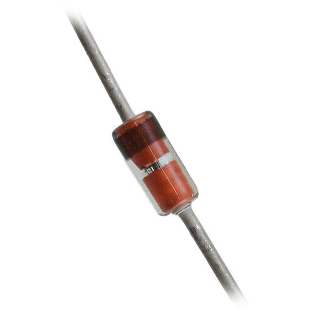
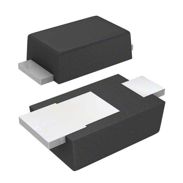
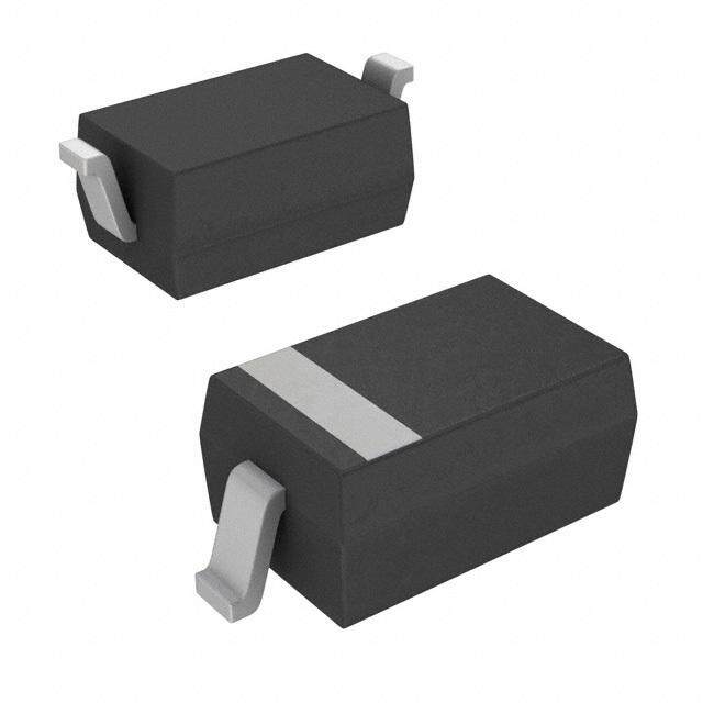
| 描述 | DIODE ZENER 500MW SOD-123稳压二极管 9.1 Volt 0.41W 5% |
| 产品分类 | 单二极管/齐纳分离式半导体 |
| 品牌 | Vishay SemiconductorsVishay Semiconductor Diodes Division |
| 产品手册 | |
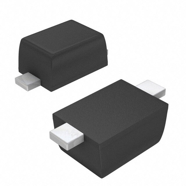
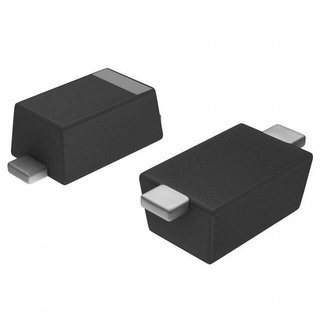
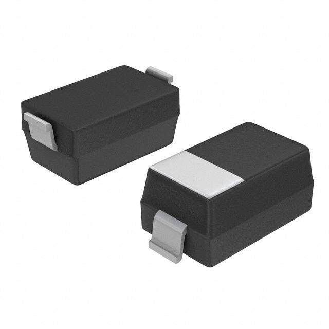
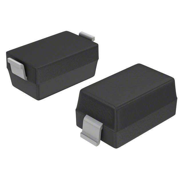
| 产品图片 | |
| rohs | 符合RoHS无铅 / 符合限制有害物质指令(RoHS)规范要求 |
| 产品系列 | 二极管与整流器,稳压二极管,Vishay Semiconductors BZT52C9V1-E3-08* |
| 数据手册 | |
| 产品型号 | BZT52C9V1-E3-08BZT52C9V1-E3-08 |
| 产品 | Small Signal Zener Diodes |
| 产品种类 | |
| 功率耗散 | 410 mW |
| 单位重量 | 10.300 mg |
| 商标 | Vishay Semiconductors |
| 安装风格 | SMD/SMT |
| 封装 | Reel |
| 封装/箱体 | SOD-123-2 |
| 工厂包装数量 | 3000 |
| 最大反向漏泄电流 | 100 nA |
| 最大工作温度 | + 150 C |
| 最大齐纳阻抗 | 10 Ohms |
| 最小工作温度 | - 55 C |
| 标准包装 | 3,000 |
| 电压容差 | 5 % |
| 电压温度系数 | 0.8 mV/C |
| 系列 | BZT52 |
| 配置 | Single |
| 齐纳电压 | 9.1 V |
| 齐纳电流 | 36 mA |


- 商务部:美国ITC正式对集成电路等产品启动337调查
- 曝三星4nm工艺存在良率问题 高通将骁龙8 Gen1或转产台积电
- 太阳诱电将投资9.5亿元在常州建新厂生产MLCC 预计2023年完工
- 英特尔发布欧洲新工厂建设计划 深化IDM 2.0 战略
- 台积电先进制程称霸业界 有大客户加持明年业绩稳了
- 达到5530亿美元!SIA预计今年全球半导体销售额将创下新高
- 英特尔拟将自动驾驶子公司Mobileye上市 估值或超500亿美元
- 三星加码芯片和SET,合并消费电子和移动部门,撤换高东真等 CEO
- 三星电子宣布重大人事变动 还合并消费电子和移动部门
- 海关总署:前11个月进口集成电路产品价值2.52万亿元 增长14.8%


PDF Datasheet 数据手册内容提取
BZT52-Series www.vishay.com Vishay Semiconductors Small Signal Zener Diodes FEATURES • Silicon planar Zener diodes Available • The Zener voltages are graded according to the international E24 standard • AEC-Q101 qualified available • ESD capability according to AEC-Q101: Human body model > 8 kV Machine model > 800 V DESIGN SUPPORT TOOLS click logo to get started • Base P/N-E3 - RoHS-compliant, commercial grade Models • Base P/N-HE3 - RoHS-compliant, AEC-Q101 qualified Available • Material categorization: for definitions of compliance PRIMARY CHARACTERISTICS please see www.vishay.com/doc?99912 PARAMETER VALUE UNIT V range nom. 2.4 to 75 V Z Test current I 2.5; 5 mA ZT V specification Pulse current Z Circuit configuration Single ORDERING INFORMATION DEVICE NAME ORDERING CODE TAPED UNITS PER REEL MINIMUM ORDER QUANTITY BZT52C2V4-E3-08 to BZT52C75-E3-08 BZT52B2V4-E3-08 to BZT52B75-E3-08 3000 (8 mm tape on 7" reel) 15 000/box BZT52C2V4-HE3-08 to BZT52C75-HE3-08 BZT52B2V4-HE3-08 to BZT52B75-HE3-08 BZT52-series BZT52C2V4-E3-18 to BZT52C75-E3-18 BZT52B2V4-E3-18 to BZT52B75-E3-18 10 000 (8 mm tape on 13" reel) 10 000/box BZT52C2V4-HE3-18 to BZT52C75-HE3-18 BZT52B2V4-HE3-18 to BZT52B75-HE3-18 PACKAGE MOLDING COMPOUND MOISTURE SENSITIVITY PACKAGE NAME WEIGHT SOLDERING CONDITIONS FLAMMABILITY RATING LEVEL MSL level 1 SOD-123 10.3 mg UL 94 V-0 260 °C/10 s at terminals (according J-STD-020) ABSOLUTE MAXIMUM RATINGS (T = 25 °C, unless otherwise specified) amb PARAMETER TEST CONDITION SYMBOL VALUE UNIT Diode on ceramic substrate 0.7 mm; P 500 mW 5 mm2 pad areas tot Power dissipation Diode on ceramic substrate 0.7 mm; P 410 mW 2.5 mm2 pad areas tot Zener current See table “Electrical Characteristics “ Valid provided that electrodes are kept at Thermal resistance junction to ambient air R 300 K/W ambient temperature thJA Junction temperature Tj 150 °C Storage temperature range Tstg -65 to +150 °C Operating temperature range Top -55 to +150 °C Rev. 1.9, 20-Feb-18 1 Document Number: 85760 For technical questions within your region: DiodesAmericas@vishay.com, DiodesAsia@vishay.com, DiodesEurope@vishay.com THIS DOCUMENT IS SUBJECT TO CHANGE WITHOUT NOTICE. THE PRODUCTS DESCRIBED HEREIN AND THIS DOCUMENT ARE SUBJECT TO SPECIFIC DISCLAIMERS, SET FORTH AT www.vishay.com/doc?91000
BZT52-Series www.vishay.com Vishay Semiconductors ELECTRICAL CHARACTERISTICS (T = 25 °C, unless otherwise specified) amb ZENER VOLTAGE TEST REVERSE DYNAMIC TEMP. ADMISSABLE ZENER RANGE (1) CURRENT VOLTAGE RESISTANCE COEFFICIENT CURRENT (4) PNAURMTB ER MACROKDIENG VZ at IZT1 IZT1 IZT2 VR at IR ZIZZT a1t ZIZZKT 2at VZ TambIZ = a 4t5 °CTambIZ = a 2t5 °C V mA V nA 10-4/°C mA MIN. NOM. MAX. BZT52C2V4 W1 2.2 2.4 2.6 5 1 - - 85 600 -9 to -4 - - BZT52C2V7 W2 2.5 2.7 2.9 5 1 - - 75 (< 83) < 500 -9 to -4 113 134 BZT52C3V0 W3 2.8 3.0 3.2 5 1 - - 80 (< 95) < 500 -9 to -3 98 118 BZT52C3V3 W4 3.1 3.3 3.5 5 1 - - 80 (< 95) < 500 -8 to -3 92 109 BZT52C3V6 W5 3.4 3.6 3.8 5 1 - - 80 (< 95) < 500 -8 to -3 85 100 BZT52C3V9 W6 3.7 3.9 4.1 5 1 - - 80 (< 95) < 500 -7 to -3 77 92 BZT52C4V3 W7 4 4.3 4.6 5 1 - - 80 (< 95) < 500 -6 to -1 71 84 BZT52C4V7 W8 4.4 4.7 5 5 1 - - 70 (< 78) < 500 -5 to +2 64 76 BZT52C5V1 W9 4.8 5.1 5.4 5 1 > 0.8 100 30 (< 60) < 480 -3 to +4 56 67 BZT52C5V6 WA 5.2 5.6 6 5 1 > 1 100 10 (< 40) < 400 -2 to +6 50 59 BZT52C6V2 WB 5.8 6.2 6.6 5 1 > 2 100 4.8 (< 10) < 200 -1 to +7 45 54 BZT52C6V8 WC 6.4 6.8 7.2 5 1 > 3 100 4.5 (< 8) < 150 +2 to +7 41 49 BZT52C7V5 WD 7 7.5 7.9 5 1 > 5 100 4 (< 7) < 50 +3 to +7 37 44 BZT52C8V2 WE 7.7 8.2 8.7 5 1 > 6 100 4.5 (< 7) < 50 +4 to +7 34 40 BZT52C9V1 WF 8.5 9.1 9.6 5 1 > 7 100 4.8 (< 10) < 50 +5 to +8 30 36 BZT52C10 WG 9.4 10 10.6 5 1 > 7.5 100 5.2 (< 15) < 70 +5 to +8 28 33 BZT52C11 WH 10.4 11 11.6 5 1 > 8.5 100 6 (< 20) < 70 +5 to +9 25 30 BZT52C12 WI 11.4 12 12.7 5 1 > 9 100 7 (< 20) < 90 +6 to +9 23 28 BZT52C13 WK 12.4 13 14.1 5 1 > 10 100 9 (< 25) < 110 +7 to +9 21 25 BZT52C15 WL 13.8 15 15.6 5 1 > 11 100 11 (< 30) < 110 +7 to +9 19 23 BZT52C16 WM 15.3 16 17.1 5 1 > 12 100 13 (< 40) < 170 +8 to +9.5 17 20 BZT52C18 WN 16.8 18 19.1 5 1 > 14 100 18 (< 50) < 170 +8 to +9.5 15 18 BZT52C20 WO 18.8 20 21.2 5 1 > 15 100 20 (< 50) < 220 +8 to +10 14 17 BZT52C22 WP 20.8 22 23.3 5 1 > 17 100 25 (< 55) < 220 +8 to +10 13 16 BZT52C24 WR 22.8 24 25.6 5 1 > 18 100 28 (< 80) < 220 +8 to +10 11 13 BZT52C27 WS 25.1 27 28.9 5 1 > 20 100 30 (< 80) < 250 +8 to +10 10 12 BZT52C30 WT 28 30 32 5 1 > 22.5 100 35 (< 80) < 250 +8 to +10 9 10 BZT52C33 WU 31 33 35 5 1 > 25 100 40 (< 80) < 250 +8 to +10 8 9 BZT52C36 WW 34 36 38 5 1 > 27 100 40 (< 90) < 250 +8 to +10 8 9 BZT52C39 WX 37 39 41 5 1 > 29 100 50 (< 90) < 300 +10 to +12 7 8 BZT52C43 WY 40 43 46 5 1 > 32 100 60 (< 100) < 700 +10 to +12 6 7 BZT52C47 WZ 44 47 50 5 1 > 35 100 70 (< 100) < 750 +10 to +12 5 6 BZT52C51 X1 48 51 54 5 1 > 38 100 70 (< 100) < 750 +10 to +12 5 6 BZT52C56 X2 52 56 60 2.5 0.5 - - < 135 (2) < 1000 (3) typ. +10 (2) - - BZT52C62 X3 58 62 66 2.5 0.5 - - < 150 (2) < 1000 (3) typ. +10 (2) - - BZT52C68 X4 64 68 72 2.5 0.5 - - < 200 (2) < 1000 (3) typ. +10 (2) - - BZT52C75 X5 70 75 79 2.5 0.5 - - < 250 (2) < 1500 (3) typ. +10 (2) - - Notes • I = 5 mA, I = 1 mA ZT1 ZT2 (1) Measured with pulses t = 5 ms p (2) I = 2.5 mA ZT1 (3) I = 0.5 mA ZT2 (4) Valid provided that electrodes are kept at ambient temperature Rev. 1.9, 20-Feb-18 2 Document Number: 85760 For technical questions within your region: DiodesAmericas@vishay.com, DiodesAsia@vishay.com, DiodesEurope@vishay.com THIS DOCUMENT IS SUBJECT TO CHANGE WITHOUT NOTICE. THE PRODUCTS DESCRIBED HEREIN AND THIS DOCUMENT ARE SUBJECT TO SPECIFIC DISCLAIMERS, SET FORTH AT www.vishay.com/doc?91000
BZT52-Series www.vishay.com Vishay Semiconductors ELECTRICAL CHARACTERISTICS (T = 25 °C, unless otherwise specified) amb ZENER VOLTAGE TEST REVERSE DYNAMIC TEMP. ADMISSABLE ZENER RANGE (1) CURRENT VOLTAGE RESISTANCE COEFFICIENT CURRENT (4) PNAURMTB ER MACROKDIENG VZ at IZT1 IZT1 IZT2 VR at IR ZZ at IZT1 ZIZZKT 2at VZ TambIZ = a 4t5 °C TambI Z= a 2t 5 °C V mA V nA 10-4/°C mA MIN. NOM. MAX. BZT52B2V4 W1 2.35 2.4 2.45 5 1 - - 85 600 -9 to -4 - - BZT52B2V7 W2 2.65 2.7 2.75 5 1 - - 75 (< 83) < 500 -9 to -4 113 134 BZT52B3V0 W3 2.94 3.0 3.06 5 1 - - 80 (< 95) < 500 -9 to -3 98 118 BZT52B3V3 W4 3.23 3.3 3.37 5 1 - - 80 (< 95) < 500 -8 to -3 92 109 BZT52B3V6 W5 3.53 3.6 3.67 5 1 - - 80 (< 95) < 500 -8 to -3 85 100 BZT52B3V9 W6 3.82 3.9 3.98 5 1 - - 80 (< 95) < 500 -7 to -3 77 92 BZT52B4V3 W7 4.21 4.3 4.39 5 1 - - 80 (< 95) < 500 -6 to -1 71 84 BZT52B4V7 W8 4.61 4.7 4.79 5 1 - - 70 (< 78) < 500 -5 to +2 64 76 BZT52B5V1 W9 5 5.1 5.2 5 1 > 0.8 100 30 (< 60) < 480 -3 to +4 56 67 BZT52B5V6 WA 5.49 5.6 5.71 5 1 > 1 100 10 (< 40) < 400 -2 to +6 50 59 BZT52B6V2 WB 6.08 6.2 6.32 5 1 > 2 100 4.8 (< 10) < 200 -1 to +7 45 54 BZT52B6V8 WC 6.66 6.8 6.94 5 1 > 3 100 4.5 (< 8) < 150 +2 to +7 41 49 BZT52B7V5 WD 7.35 7.5 7.65 5 1 > 5 100 4 (< 7) < 50 +3 to +7 37 44 BZT52B8V2 WE 8.04 8.2 8.36 5 1 > 6 100 4.5 (< 7) < 50 +4 to +7 34 40 BZT52B9V1 WF 8.92 9.1 9.28 5 1 > 7 100 4.8 (< 10) < 50 +5 to +8 30 36 BZT52B10 WG 9.8 10 10.2 5 1 > 7.5 100 5.2 (< 15) < 70 +5 to +8 28 33 BZT52B11 WH 10.8 11 11.2 5 1 > 8.5 100 6 (< 20) < 70 +5 to +9 25 30 BZT52B12 WI 11.8 12 12.2 5 1 > 9 100 7 (< 20) < 90 +6 to +9 23 28 BZT52B13 WK 12.7 13 13.3 5 1 > 10 100 9 (< 25) < 110 +7 to +9 21 25 BZT52B15 WL 14.7 15 15.3 5 1 > 11 100 11 (< 30) < 110 +7 to +9 19 23 BZT52B16 WM 15.7 16 16.3 5 1 > 12 100 13 (< 40) < 170 +8 to +9.5 17 20 BZT52B18 WN 17.6 18 18.4 5 1 > 14 100 18 (< 50) < 170 +8 to +9.5 15 18 BZT52B20 WO 19.6 20 20.4 5 1 > 15 100 20 (< 50) < 220 +8 to +10 14 17 BZT52B22 WP 21.6 22 22.4 5 1 > 17 100 25 (< 55) < 220 +8 to +10 13 16 BZT52B24 WR 23.5 24 24.5 5 1 > 18 100 28 (< 80) < 220 +8 to +10 11 13 BZT52B27 WS 26.5 27 27.5 5 1 > 20 100 30 (< 80) < 250 +8 to +10 10 12 BZT52B30 WT 29.4 30 30.6 5 1 > 22.5 100 35 (< 80) < 250 +8 to +10 9 10 BZT52B33 WU 32.3 33 33.7 5 1 > 25 100 40 (< 80) < 250 +8 to +10 8 9 BZT52B36 WW 35.3 36 36.7 5 1 > 27 100 40 (< 90) < 250 +8 to +10 8 9 BZT52B39 WX 38.2 39 39.8 5 1 > 29 100 50 (< 90) < 300 +10 to +12 7 8 BZT52B43 WY 42.1 43 43.9 5 1 > 32 100 60 (< 100) < 700 +10 to +12 6 7 BZT52B47 WZ 46.1 47 47.9 5 1 > 35 100 70 (< 100) < 750 +10 to +12 5 6 BZT52B51 X1 50 51 52 5 1 > 38 100 70 (< 100) < 750 +10 to +12 5 6 BZT52B56 X2 54.9 56 57.1 2.5 0.5 - - < 135 (2) < 1000 (3) typ. +10 (2) - - BZT52B62 X3 60.8 62 63.2 2.5 0.5 - - < 150 (2) < 1000 (3) typ. +10 (2) - - BZT52B68 X4 66.6 68 69.4 2.5 0.5 - - < 200 (2) < 1000 (3) typ. +10 (2) - - BZT52B75 X5 73.5 75 76.5 2.5 0.5 - - < 250 (2) < 1500 (3) typ. +10 (2) - - Notes • I = 5 mA, I = 1 mA ZT1 ZT2 (1) Measured with pulses t = 5 ms p (2) I = 2.5 mA ZT1 (3) I = 0.5 mA ZT2 (4) Valid provided that electrodes are kept at ambient temperature Rev. 1.9, 20-Feb-18 3 Document Number: 85760 For technical questions within your region: DiodesAmericas@vishay.com, DiodesAsia@vishay.com, DiodesEurope@vishay.com THIS DOCUMENT IS SUBJECT TO CHANGE WITHOUT NOTICE. THE PRODUCTS DESCRIBED HEREIN AND THIS DOCUMENT ARE SUBJECT TO SPECIFIC DISCLAIMERS, SET FORTH AT www.vishay.com/doc?91000
BZT52-Series www.vishay.com Vishay Semiconductors TYPICAL CHARACTERISTICS (T = 25 °C, unless otherwise specified) amb mA Ω 103 100 T = 25 °C J 102 5 4 IF 10 r 3 33 1 TJ = 100 °C zj 2 27 22 10-1 T = 25 °C 10 18 J 10-2 15 5 4 12 10-3 3 10 2 10-4 6.8/8.2 6.2 10-5 1 0 0.2 0.4 0.6 0.8 1V 0.1 2 5 1 2 5 10 2 5 100 mA 18114 V 18119 I F Z Fig. 1 - Forward characteristics Fig. 4 - Dynamic Resistance vs. Zener Current mW Ω 500 103 T = 25 °C 7 j 5 400 4 P Rzj 3 47 +4 531 tot 2 39 300 36 102 200 7 5 4 3 100 2 0 10 0 100 200 °C 0.1 2 3 4 5 1 2 3 4 5 10 18888 Tamb 18120 IZ mA Fig. 2 - Admissible Power Dissipation vs. Ambient Temperature Fig. 5 - Dynamic Resistance vs. Zener Current Ω Ω 103 1000 ΔV 5 TJ = 25 °C 54 Rzth = RthA x VZ x ΔTZ 4 3 j rzj 32 Rzth 2 100 102 54 54 3 3 2 2 10 2.7 10 3.6 5 5 4 4.7 4 3 5.1 3 negative positive 2 2 1 5.6 1 0.1 2 5 1 2 5 10 2 5 100 mA 1 2 3 4 5 10 2 3 4 5 100 V 18117 IZ 18121 VZ at IZ = 5 mA Fig. 3 - Dynamic Resistance vs. Zener Current Fig. 6 - Thermal Differential Resistance vs. Zener Voltage Rev. 1.9, 20-Feb-18 4 Document Number: 85760 For technical questions within your region: DiodesAmericas@vishay.com, DiodesAsia@vishay.com, DiodesEurope@vishay.com THIS DOCUMENT IS SUBJECT TO CHANGE WITHOUT NOTICE. THE PRODUCTS DESCRIBED HEREIN AND THIS DOCUMENT ARE SUBJECT TO SPECIFIC DISCLAIMERS, SET FORTH AT www.vishay.com/doc?91000
BZT52-Series www.vishay.com Vishay Semiconductors Ω mV/°C 100 100 I = 5 mA 7 Z 54 ΔVZ 80 Rzj 3 ΔTj 2 60 10 7 40 5 4 3 20 2 T = 25 °C Ij = 5 mA 1 Z 0 1 2 3 4 5 10 2 3 4 5 100 V 0 20 40 60 80 100 V 18122 V 18136 V at I = 2 mA Z Z Z Fig. 7 - Dynamic Resistance vs. Zener Voltage Fig. 10 - Temperature Dependence of Zener Voltage vs. Zener Voltage mV/°C V 25 9 8 ΔΔVTjZ 2105 IZ = 2015 mm mAAA ΔVZ 76 VZ at IZ = 5 mA 51 5 43 10 4 36 3 5 2 1 0 0 IZ = 5 mA - 1 - 5 0 20 40 60 80 100 120 140 °C 1 2 3 4 5 10 2 3 4 5 100 V 18158 Tj 18135 V at I = 5 mA V Z≥ 27Z V, I = 2 mA Fig. 8 - Temperature Dependence of Zener Voltage vs. Fig. 11 - Change of Zener Voltage vs. Junction Temperature Zener Voltage V V 0.8 1.6 25 15 ΔVZ = rZth x IZ 00..76 VZ at IZ = 5 mA 10 11..42 IVZZ = > 5= m56A V; IZ = 2.5 mA ΔV 0.5 ΔVZ 1.0 Z 8 0.8 0.4 7 0.6 0.3 6.2 0.4 0.2 5.9 0.2 0.1 5.6 0 0 5.1 - 0.2 - 1 - 0.4 3.6 4.7 1 10 100 V - 0.20 20 40 60 80 100 120 140 C 18159 VZ at IZ = 5 mA 18124 T j Fig. 9 - Change of Zener Voltage vs. Junction Temperature Fig. 12 - Change of Zener Voltage from Turn-on up to the Point of Thermal Equilibrium vs. Zener Voltage Rev. 1.9, 20-Feb-18 5 Document Number: 85760 For technical questions within your region: DiodesAmericas@vishay.com, DiodesAsia@vishay.com, DiodesEurope@vishay.com THIS DOCUMENT IS SUBJECT TO CHANGE WITHOUT NOTICE. THE PRODUCTS DESCRIBED HEREIN AND THIS DOCUMENT ARE SUBJECT TO SPECIFIC DISCLAIMERS, SET FORTH AT www.vishay.com/doc?91000
BZT52-Series www.vishay.com Vishay Semiconductors V mA 5 ΔVZ = rzth x IZ 50 Tj = 25 °C2.7 3.9 5.6 3.3 4.7 6.8 4 40 ΔV lZ 8.2 Z 3 30 I = 5 mA Z 2 20 Test 1 I = 2.5 mA 10 cIu5rr emnAt Z Z 0 0 0 20 40 60 80 100 V 0 1 2 3 4 5 6 7 8 9 10 V 18160 VZ at IZ = 5 mA 18111 VZ Fig. 13 - Change of Zener Voltage from Turn-on up to the Point of Fig. 14 - Breakdown Characteristics Thermal Equilibrium vs. Zener Voltage mA 30 10 12 Tj = 25 °C lZ 15 20 18 22 Test 27 10 current 3336 IZ 5 mA 0 0 10 20 30 40 V 18112 VZ Fig. 15 - Breakdown Characteristics 18157 Fig. 16 - Breakdown Characteristics Rev. 1.9, 20-Feb-18 6 Document Number: 85760 For technical questions within your region: DiodesAmericas@vishay.com, DiodesAsia@vishay.com, DiodesEurope@vishay.com THIS DOCUMENT IS SUBJECT TO CHANGE WITHOUT NOTICE. THE PRODUCTS DESCRIBED HEREIN AND THIS DOCUMENT ARE SUBJECT TO SPECIFIC DISCLAIMERS, SET FORTH AT www.vishay.com/doc?91000
BZT52-Series www.vishay.com Vishay Semiconductors PACKAGE DIMENSIONS in millimeters (inches): SOD-123 x. a m 4) 0 0 0. 1 ( 0. 1.35 (0.053) 1 (0.039) 0.2 (0.008) 00..4255 ((00..001180)) 0° to 8° 0.15 (0.006) 0.10 (0.004) 0.5 (0.020) ref. Cathode bar Mounting Pad Layout 2.85 (0.112) 2.55 (0.100) 0.85 (0.033) 0.85 (0.033) 0.65 (0.026) 0.45 (0.018) 33..8555 ((00..115420)) 1.7 (0.067) 1.40 (0.055) 2.5 (0.098) 0.85 (0.033) Rev. 4 - Date: 24. Sep. 2009 Document no.: S8-V-3910.01-001 (4) 17432 Rev. 1.9, 20-Feb-18 7 Document Number: 85760 For technical questions within your region: DiodesAmericas@vishay.com, DiodesAsia@vishay.com, DiodesEurope@vishay.com THIS DOCUMENT IS SUBJECT TO CHANGE WITHOUT NOTICE. THE PRODUCTS DESCRIBED HEREIN AND THIS DOCUMENT ARE SUBJECT TO SPECIFIC DISCLAIMERS, SET FORTH AT www.vishay.com/doc?91000
Legal Disclaimer Notice www.vishay.com Vishay Disclaimer ALL PRODUCT, PRODUCT SPECIFICATIONS AND DATA ARE SUBJECT TO CHANGE WITHOUT NOTICE TO IMPROVE RELIABILITY, FUNCTION OR DESIGN OR OTHERWISE. Vishay Intertechnology, Inc., its affiliates, agents, and employees, and all persons acting on its or their behalf (collectively, “Vishay”), disclaim any and all liability for any errors, inaccuracies or incompleteness contained in any datasheet or in any other disclosure relating to any product. Vishay makes no warranty, representation or guarantee regarding the suitability of the products for any particular purpose or the continuing production of any product. To the maximum extent permitted by applicable law, Vishay disclaims (i) any and all liability arising out of the application or use of any product, (ii) any and all liability, including without limitation special, consequential or incidental damages, and (iii) any and all implied warranties, including warranties of fitness for particular purpose, non-infringement and merchantability. Statements regarding the suitability of products for certain types of applications are based on Vishay’s knowledge of typical requirements that are often placed on Vishay products in generic applications. Such statements are not binding statements about the suitability of products for a particular application. It is the customer’s responsibility to validate that a particular product with the properties described in the product specification is suitable for use in a particular application. Parameters provided in datasheets and / or specifications may vary in different applications and performance may vary over time. All operating parameters, including typical parameters, must be validated for each customer application by the customer’s technical experts. Product specifications do not expand or otherwise modify Vishay’s terms and conditions of purchase, including but not limited to the warranty expressed therein. Except as expressly indicated in writing, Vishay products are not designed for use in medical, life-saving, or life-sustaining applications or for any other application in which the failure of the Vishay product could result in personal injury or death. Customers using or selling Vishay products not expressly indicated for use in such applications do so at their own risk. Please contact authorized Vishay personnel to obtain written terms and conditions regarding products designed for such applications. No license, express or implied, by estoppel or otherwise, to any intellectual property rights is granted by this document or by any conduct of Vishay. Product names and markings noted herein may be trademarks of their respective owners. © 2017 VISHAY INTERTECHNOLOGY, INC. ALL RIGHTS RESERVED Revision: 08-Feb-17 1 Document Number: 91000
Mouser Electronics Authorized Distributor Click to View Pricing, Inventory, Delivery & Lifecycle Information: V ishay: BZT52C24-GS08 BZT52C8V2-V-GS08 BZT52C36-V-GS08 BZT52C12-V-GS08 BZT52C24-V-GS08 BZT52C9V1- V-GS08 BZT52C16-V-GS08 BZT52C13-V-GS08 BZT52C10-V-GS08 BZT52C22-V-GS08 BZT52C4V3-V-GS08 BZT52C27-V-GS08 BZT52C5V6-V-GS08 BZT52C3V9-V-GS08 BZT52C30-V-GS08 BZT52B10-V-GS08 BZT52B10- V-GS18 BZT52B11-V-GS08 BZT52B11-V-GS18 BZT52B12-V-GS08 BZT52B12-V-GS18 BZT52B13-V-GS08 BZT52B13-V-GS18 BZT52B15-V-GS08 BZT52B15-V-GS18 BZT52B16-V-GS08 BZT52B16-V-GS18 BZT52B18-V- GS08 BZT52B18-V-GS18 BZT52B2V4-V-GS08 BZT52B2V4-V-GS18 BZT52B2V7-V-GS08 BZT52B2V7-V-GS18 BZT52B20-V-GS08 BZT52B20-V-GS18 BZT52B22-V-GS08 BZT52B22-V-GS18 BZT52B24-V-GS08 BZT52B24-V- GS18 BZT52B27-V-GS08 BZT52B27-V-GS18 BZT52B3V0-V-GS08 BZT52B3V0-V-GS18 BZT52B3V3-V-GS08 BZT52B3V3-V-GS18 BZT52B3V6-V-GS08 BZT52B3V6-V-GS18 BZT52B3V9-V-GS08 BZT52B3V9-V-GS18 BZT52B30-V-GS08 BZT52B30-V-GS18 BZT52B33-V-GS08 BZT52B33-V-GS18 BZT52B36-V-GS08 BZT52B36-V- GS18 BZT52B39-V-GS08 BZT52B39-V-GS18 BZT52B4V3-V-GS08 BZT52B4V3-V-GS18 BZT52B4V7-V-GS08 BZT52B4V7-V-GS18 BZT52B43-V-GS08 BZT52B43-V-GS18 BZT52B47-V-GS08 BZT52B47-V-GS18 BZT52B5V1- V-GS08 BZT52B5V1-V-GS18 BZT52B5V6-V-GS08 BZT52B5V6-V-GS18 BZT52B51-V-GS08 BZT52B51-V-GS18 BZT52B56-V-GS08 BZT52B56-V-GS18 BZT52B6V2-V-GS08 BZT52B6V2-V-GS18 BZT52B6V8-V-GS08 BZT52B6V8-V-GS18 BZT52B62-V-GS08 BZT52B62-V-GS18 BZT52B68-V-GS08 BZT52B68-V-GS18 BZT52B7V5- V-GS08 BZT52B7V5-V-GS18 BZT52B75-V-GS08 BZT52B75-V-GS18 BZT52B8V2-V-GS08 BZT52B8V2-V-GS18 BZT52B9V1-V-GS08 BZT52B9V1-V-GS18 BZT52C10-V-GS18 BZT52C11-V-GS18 BZT52C12-V-GS18 BZT52C13- V-GS18 BZT52C16-V-GS18 BZT52C18-V-GS18 BZT52C2V4-V-GS18 BZT52C2V7-V-GS18 BZT52C20-V-GS18 BZT52C24-V-GS18 BZT52C27-V-GS18