ICGOO在线商城 > BZA456A,115

 Datasheet下载
- 型号: BZA456A,115
- 制造商: NXP Semiconductors
- 库位|库存: xxxx|xxxx
- 要求:
| 数量阶梯 | 香港交货 | 国内含税 |
| +xxxx | $xxxx | ¥xxxx |
查看当月历史价格
查看今年历史价格
BZA456A,115产品简介:
ICGOO电子元器件商城为您提供BZA456A,115由NXP Semiconductors设计生产,在icgoo商城现货销售,并且可以通过原厂、代理商等渠道进行代购。 提供BZA456A,115价格参考以及NXP SemiconductorsBZA456A,115封装/规格参数等产品信息。 你可以下载BZA456A,115参考资料、Datasheet数据手册功能说明书, 资料中有BZA456A,115详细功能的应用电路图电压和使用方法及教程。
| 参数 | 数值 |
| 产品目录 | |
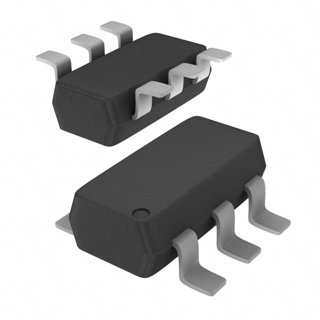
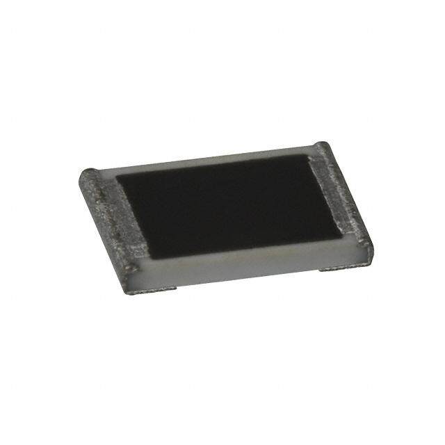
| 描述 | TVS DIODE 5.6VWM 8VC 6TSOPTVS二极管阵列 DIODE ARRAY TAPE-7 |
| 产品分类 | |
| 品牌 | NXP Semiconductors |
| 产品手册 | |
| 产品图片 |
|
| rohs | 符合RoHS无铅 / 符合限制有害物质指令(RoHS)规范要求 |
| 产品系列 | 二极管与整流器,TVS二极管,TVS二极管阵列,NXP Semiconductors BZA456A,115- |
| 数据手册 | |
| 产品型号 | BZA456A,115 |
| PCN封装 | |
| PCN设计/规格 | |
| 不同频率时的电容 | 240pF @ 1MHz |
| 产品种类 | TVS二极管阵列 |
| 供应商器件封装 | 6-TSOP |
| 其它名称 | 568-6240-1 |
| 功率-峰值脉冲 | 24W |
| 包装 | 剪切带 (CT) |
| 单向通道 | 4 |
| 双向通道 | - |
| 商标 | NXP Semiconductors |
| 安装类型 | 表面贴装 |
| 安装风格 | SMD/SMT |
| 封装 | Reel |
| 封装/外壳 | SC-74,SOT-457 |
| 封装/箱体 | SOT-457 |
| 尺寸 | 1.7 mm W x 3.1 mm L x 1.1 mm H |
| 峰值浪涌电流 | 3 A |
| 峰值脉冲功率耗散 | 24 W |
| 工作温度 | -65°C ~ 150°C (TJ) |
| 工作电压 | 5.88 V |
| 工厂包装数量 | 3000 |
| 应用 | 通用 |
| 最大工作温度 | + 150 C |
| 最小工作温度 | - 65 C |
| 极性 | Unidirectional |
| 标准包装 | 1 |
| 电压-击穿(最小值) | - |
| 电压-反向关态(典型值) | 5.6V |
| 电压-箝位(最大值)@Ipp | 8V |
| 电容 | 240 pF |
| 电流-峰值脉冲(10/1000µs) | 3A (8/20µs) |
| 电源线路保护 | 无 |
| 端接类型 | SMD/SMT |
| 类型 | 齐纳 |
| 系列 | BZA456A |
| 通道 | 4 Channels |
| 钳位电压 | 8 V |
| 零件号别名 | BZA456A T/R |


PDF Datasheet 数据手册内容提取
Important notice Dear Customer, On 7 February 2017 the former NXP Standard Product business became a new company with the tradename Nexperia. Nexperia is an industry leading supplier of Discrete, Logic and PowerMOS semiconductors with its focus on the automotive, industrial, computing, consumer and wearable application markets In data sheets and application notes which still contain NXP or Philips Semiconductors references, use the references to Nexperia, as shown below. Instead of http://www.nxp.com, http://www.philips.com/ or http://www.semiconductors.philips.com/, use http://www.nexperia.com Instead of sales.addresses@www.nxp.com or sales.addresses@www.semiconductors.philips.com, use salesaddresses@nexperia.com (email) Replace the copyright notice at the bottom of each page or elsewhere in the document, depending on the version, as shown below: - © NXP N.V. (year). All rights reserved or © Koninklijke Philips Electronics N.V. (year). All rights reserved Should be replaced with: - © Nexperia B.V. (year). All rights reserved. If you have any questions related to the data sheet, please contact our nearest sales office via e-mail or telephone (details via salesaddresses@nexperia.com). Thank you for your cooperation and understanding, Kind regards, Team Nexperia
DISCRETE SEMICONDUCTORS DATA SHEET dbook, halfpage M3D302 BZA456A Quadruple ESD transient voltage suppressor Product data sheet 1999 May 25 Supersedes data of 1998 Oct 30
NXP Semiconductors Product data sheet Quadruple ESD transient voltage BZA456A suppressor FEATURES PINNING • ESD rating >8 kV, according to IEC1000-4-2 PIN DESCRIPTION • SOT457 surface mount package 1 cathode 1 • Common anode configuration 2 common • Non-clamping range −0.5 to 5.6 V 3 cathode 2 • Maximum reverse peak power dissipation: 4 cathode 3 24 W at t = 1 ms p 5 common • Maximum clamping voltage at peak pulse current: 6 cathode 4 8 V at I = 3 A. ZSM APPLICATIONS • Computers and peripherals handbook, halfpag6e 5 4 1 • Audio and video equipment 3 2 • Communication systems 4 5 • Medical equipment. 6 1 2 3 DESCRIPTION Top view MAM357 Monolithic transient voltage suppressor diode in a six lead SOT457 (SC-74) package for 4-bit wide ESD transient Marking code: Z6. suppression at 5.6 V level. Fig.1 Simplified outline (SOT457) and symbol. LIMITING VALUES In accordance with the Absolute Maximum Rating System (IEC 134). SYMBOL PARAMETER CONDITIONS MIN. MAX. UNIT Per diode I working current T = 60 °C; note 1 − note 2 mA Z s I continuous forward current T = 60 °C − 100 mA F s I non-repetitive peak forward current t = 1 ms; square pulse − 3.75 A FSM p I non-repetitive peak reverse current t = 1 ms; square pulse; see Fig.2 − 3 A ZSM p P total power dissipation T = 60 °C; see Fig.3 − 720 mW tot s P non repetitive peak reverse power square pulse; t = 1 ms; see Fig.4 − 24 W ZSM p dissipation T storage temperature −65 +150 °C stg T junction temperature −65 +150 °C j Notes 1. T is the temperature at the soldering point of the anode pin. s 2. DC working current limited by P . tot max 1999 May 25 2
NXP Semiconductors Product data sheet Quadruple ESD transient voltage BZA456A suppressor THERMAL CHARACTERISTICS SYMBOL PARAMETER CONDITIONS VALUE UNIT R thermal resistance from junction to soldering point one or more diodes loaded 125 K/W th j-s ELECTRICAL CHARACTERISTICS T = 25 °C unless otherwise specified. j SYMBOL PARAMETER CONDITIONS MIN. TYP. MAX. UNIT Per diode V working voltage I = 1 mA 5.32 5.6 5.88 V Z Z V forward voltage I = 200 mA − − 1.3 V F F V non-repetitive peak reverse voltage I = 3 A; t = 1 ms − − 8 V ZSM ZSM p I reverse current V = 3 V − − 2 µA R R r differential resistance I = 250 µA − − 1600 Ω dif Z I = 1 mA − − 400 Ω Z S temperature coefficient of working I = 5 mA − 1.2 − mV/K Z Z voltage C diode capacitance see Fig.5 d V = 0; f = 1 MHz − − 240 pF R V = 3 V; f = 1 MHz − − 140 pF R 1999 May 25 3
NXP Semiconductors Product data sheet Quadruple ESD transient voltage BZA456A suppressor MDA190 MDA198 10 1000 handbook, halfpage handbook, halfpage Ptot (mW) 800 600 IZSM (A) 400 200 1 0 10−1 1 10 0 50 100 150 200 tp (ms) Ts (oC) All diodes loaded. Fig.2 Maximum non-repetitive peak reverse current as a function of pulse time. Fig.3 Power derating curve. 102 MDA199 250 MDA192 handbook, halfpage handbook, halfpage Cd (pF) PZSM 200 (W) 150 10 100 50 110−1 1 10 00 1 2 3 4 5 tp (ms) VR (V) PZSM = VZSM × IZSM. VZSM is the non-repetitive peak reverse voltage at IZSM. Tj = 25 °C; f = 1 MHz. Fig.4 Maximum non-repetitive peak reverse power dissipation as a function of pulse Fig.5 Diode capacitance as a function of reverse duration (square pulse). voltage; typical values. 1999 May 25 4
NXP Semiconductors Product data sheet Quadruple ESD transient voltage BZA456A suppressor handbook, full pagewidth ESD TESTER RG 223/U DIGITIZING RZ 450 Ω 50 Ω coax 10× OSCILLOSCOPE ATTENUATOR CZ note 1 50 Ω Note 1: attenuator is only used for open socket high voltage measurements IEC 1000-4-2 network CZ = 150 pF; RZ = 330 Ω 1/4 BZA456A vertical scale = 100 V/Div vertical scale = 10 V/Div horizontal scale = 50 ns/Div horizontal scale = 50 ns/Div GND GND unclamped +1 kV ESD voltage waveform clamped +1 kV ESD voltage waveform (IEC 1000−4−2 network) (IEC 1000−4−2 network) GND GND vertical scale = 100 V/Div vertical scale = 10 V/Div horizontal scale = 50 ns/Div horizontal scale = 50 ns/Div unclamped −1 kV ESD voltage waveform clamped −1 kV ESD voltage waveform (IEC 1000−4−2 network) (IEC 1000−4−2 network) MGL247 Fig.6 ESD clamping test set-up and waveforms. 1999 May 25 5
NXP Semiconductors Product data sheet Quadruple ESD transient voltage BZA456A suppressor APPLICATION INFORMATION Typical common anode application A quadruple transient suppressor in a SOT457 package makes it possible to protect four separate lines using only one package. Two simplified examples are shown in Figs 7 and 8. handbook, full pagewidth A B keyboard, C terminal, I/O D printer, etc. FUNCTIONAL DECODER BZA456A GND MGK458 Fig.7 Computer interface protection. handbook, full pagewidth VDD VGG address bus RAM ROM I/O data bus CPU CLOCK control bus BZA456A GND MGK459 Fig.8 Microprocessor protection. 1999 May 25 6
NXP Semiconductors Product data sheet Quadruple ESD transient voltage BZA456A suppressor Device placement and printed-circuit board layout Circuit board layout is of extreme importance in the suppression of transients. The clamping voltage of the BZA456A is determined by the peak transient current and the rate of rise of that current (di/dt). Since parasitic inductances can further add to the clamping voltage (V = L di/dt) the series conductor lengths on the printed-circuit board should be kept to a minimum. This includes the lead length of the suppression element. In addition to minimizing conductor length the following printed-circuit board layout guidelines are recommended: 1. Place the suppression element close to the input terminals or connectors. 2. Keep parallel signal paths to a minimum. 3. Avoid running protection conductors in parallel with unprotected conductors. 4. Minimize all printed-circuit board loop areas including power and ground loops. 5. Minimize the length of the transient return path to ground. 6. Avoid using shared transient return paths to a common ground point. 1999 May 25 7
NXP Semiconductors Product data sheet Quadruple ESD transient voltage BZA456A suppressor PACKAGE OUTLINE Plastic surface mounted package; 6 leads SOT457 D B E A X y HE v M A 6 5 4 Q pin 1 index A A1 c 1 2 3 Lp e bp w M B detail X 0 1 2 mm scale DIMENSIONS (mm are the original dimensions) UNIT A A1 bp c D E e HE Lp Q v w y 1.1 0.1 0.40 0.26 3.1 1.7 3.0 0.6 0.33 mm 0.95 0.2 0.2 0.1 0.9 0.013 0.25 0.10 2.7 1.3 2.5 0.2 0.23 OUTLINE REFERENCES EUROPEAN ISSUE DATE VERSION IEC JEDEC EIAJ PROJECTION 97-02-28 SOT457 SC-74 01-05-04 1999 May 25 8
NXP Semiconductors Product data sheet Quadruple ESD transient voltage BZA456A suppressor DATA SHEET STATUS DOCUMENT PRODUCT DEFINITION STATUS(1) STATUS(2) Objective data sheet Development This document contains data from the objective specification for product development. Preliminary data sheet Qualification This document contains data from the preliminary specification. Product data sheet Production This document contains the product specification. Notes 1. Please consult the most recently issued document before initiating or completing a design. 2. The product status of device(s) described in this document may have changed since this document was published and may differ in case of multiple devices. The latest product status information is available on the Internet at URL http://www.nxp.com. DISCLAIMERS above those given in the Characteristics sections of this document is not implied. Exposure to limiting values for General ⎯ Information in this document is believed to be extended periods may affect device reliability. accurate and reliable. However, NXP Semiconductors does not give any representations or warranties, Terms and conditions of sale ⎯ NXP Semiconductors expressed or implied, as to the accuracy or completeness products are sold subject to the general terms and of such information and shall have no liability for the conditions of commercial sale, as published at consequences of use of such information. http://www.nxp.com/profile/terms, including those pertaining to warranty, intellectual property rights Right to make changes ⎯ NXP Semiconductors infringement and limitation of liability, unless explicitly reserves the right to make changes to information otherwise agreed to in writing by NXP Semiconductors. In published in this document, including without limitation case of any inconsistency or conflict between information specifications and product descriptions, at any time and in this document and such terms and conditions, the latter without notice. This document supersedes and replaces all will prevail. information supplied prior to the publication hereof. No offer to sell or license ⎯ Nothing in this document Suitability for use ⎯ NXP Semiconductors products are may be interpreted or construed as an offer to sell products not designed, authorized or warranted to be suitable for that is open for acceptance or the grant, conveyance or use in medical, military, aircraft, space or life support implication of any license under any copyrights, patents or equipment, nor in applications where failure or malfunction other industrial or intellectual property rights. of an NXP Semiconductors product can reasonably be expected to result in personal injury, death or severe Export control ⎯ This document as well as the item(s) property or environmental damage. NXP Semiconductors described herein may be subject to export control accepts no liability for inclusion and/or use of NXP regulations. Export might require a prior authorization from Semiconductors products in such equipment or national authorities. applications and therefore such inclusion and/or use is at Quick reference data ⎯ The Quick reference data is an the customer’s own risk. extract of the product data given in the Limiting values and Applications ⎯ Applications that are described herein for Characteristics sections of this document, and as such is any of these products are for illustrative purposes only. not complete, exhaustive or legally binding. NXP Semiconductors makes no representation or warranty that such applications will be suitable for the specified use without further testing or modification. Limiting values ⎯ Stress above one or more limiting values (as defined in the Absolute Maximum Ratings System of IEC 60134) may cause permanent damage to the device. Limiting values are stress ratings only and operation of the device at these or any other conditions 1999 May 25 9
NXP Semiconductors Customer notification This data sheet was changed to reflect the new company name NXP Semiconductors, including new legal definitions and disclaimers. No changes were made to the technical content, except for package outline drawings which were updated to the latest version. Contact information For additional information please visit: http://www.nxp.com For sales offices addresses send e-mail to: salesaddresses@nxp.com © NXP B.V. 2009 All rights are reserved. Reproduction in whole or in part is prohibited without the prior written consent of the copyright owner. The information presented in this document does not form part of any quotation or contract, is believed to be accurate and reliable and may be changed without notice. No liability will be accepted by the publisher for any consequence of its use. Publication thereof does not convey nor imply any license under patent- or other industrial or intellectual property rights. Printed in The Netherlands 115002/00/03/pp10 Date of release: 1999 May 25 Document order number: 9397 750 05953