ICGOO在线商城 > 分立半导体产品 > 二极管 - 整流器 - 单 > BY229B-400HE3/81

 Datasheet下载
- 型号: BY229B-400HE3/81
- 制造商: Vishay
- 库位|库存: xxxx|xxxx
- 要求:
| 数量阶梯 | 香港交货 | 国内含税 |
| +xxxx | $xxxx | ¥xxxx |
查看当月历史价格
查看今年历史价格
BY229B-400HE3/81产品简介:
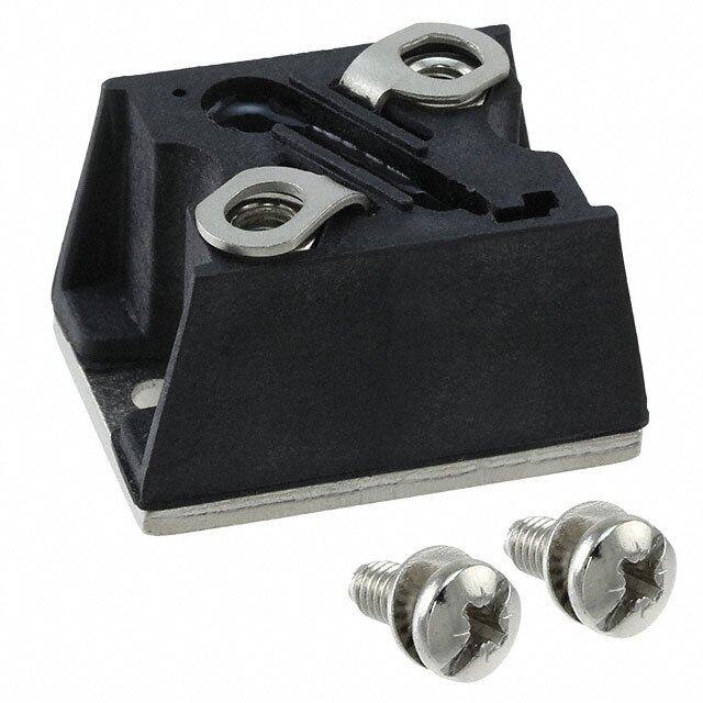
ICGOO电子元器件商城为您提供BY229B-400HE3/81由Vishay设计生产,在icgoo商城现货销售,并且可以通过原厂、代理商等渠道进行代购。 BY229B-400HE3/81价格参考。VishayBY229B-400HE3/81封装/规格:二极管 - 整流器 - 单, 标准 表面贴装 二极管 400V 8A TO-263AB。您可以下载BY229B-400HE3/81参考资料、Datasheet数据手册功能说明书,资料中有BY229B-400HE3/81 详细功能的应用电路图电压和使用方法及教程。
| 参数 | 数值 |
| 产品目录 | |
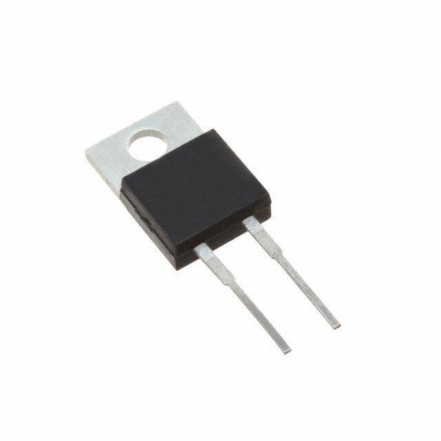
| 描述 | DIODE SWITCHING 400V 8A TO263AB整流器 8.0A 400 Volt 145ns 100 Amp IFSM |
| 产品分类 | 单二极管/整流器分离式半导体 |
| 品牌 | Vishay Semiconductor Diodes DivisionVishay Semiconductors |
| 产品手册 | |
| 产品图片 |
|
| rohs | RoHS 合规性豁免无铅 / 符合限制有害物质指令(RoHS)规范要求 |
| 产品系列 | 二极管与整流器,整流器,Vishay Semiconductors BY229B-400HE3/81- |
| 数据手册 | |
| 产品型号 | BY229B-400HE3/81BY229B-400HE3/81 |
| 不同If时的电压-正向(Vf) | 1.85V @ 20A |
| 不同 Vr、F时的电容 | - |
| 不同 Vr时的电流-反向漏电流 | 10µA @ 400V |
| 二极管类型 | 标准 |
| 产品 | Fast Recovery Rectifiers |
| 产品种类 | 整流器 |
| 供应商器件封装 | TO-263AB |
| 包装 | 带卷 (TR) |
| 反向恢复时间(trr) | 145ns |
| 反向电压 | 400 V |
| 反向电流IR | 10 uA |
| 商标 | Vishay Semiconductors |
| 安装类型 | 表面贴装 |
| 安装风格 | SMD/SMT |
| 封装 | Reel |
| 封装/外壳 | TO-263-3,D²Pak(2 引线+接片),TO-263AB |
| 封装/箱体 | TO-263AB |
| 工作温度-结 | -40°C ~ 150°C |
| 工厂包装数量 | 800 |
| 恢复时间 | 145 ns |
| 最大工作温度 | + 150 C |
| 最大浪涌电流 | 100 A |
| 最小工作温度 | - 40 C |
| 标准包装 | 800 |
| 正向电压下降 | 1.85 V |
| 正向连续电流 | 100 A |
| 电压-DC反向(Vr)(最大值) | 400V |
| 电流-平均整流(Io) | 8A |
| 速度 | 快速恢复 =< 500 ns,> 200mA(Io) |


- 商务部:美国ITC正式对集成电路等产品启动337调查
- 曝三星4nm工艺存在良率问题 高通将骁龙8 Gen1或转产台积电
- 太阳诱电将投资9.5亿元在常州建新厂生产MLCC 预计2023年完工
- 英特尔发布欧洲新工厂建设计划 深化IDM 2.0 战略
- 台积电先进制程称霸业界 有大客户加持明年业绩稳了
- 达到5530亿美元!SIA预计今年全球半导体销售额将创下新高
- 英特尔拟将自动驾驶子公司Mobileye上市 估值或超500亿美元
- 三星加码芯片和SET,合并消费电子和移动部门,撤换高东真等 CEO
- 三星电子宣布重大人事变动 还合并消费电子和移动部门
- 海关总署:前11个月进口集成电路产品价值2.52万亿元 增长14.8%

PDF Datasheet 数据手册内容提取
BY229(X,B)-200 thru BY229(X,B)-800 Vishay General Semiconductor Fast Switching Plastic Rectifier FEATURES TO-220AC ITO-220AC • Glass passivated chip junction (cid:129) Superfast recovery time for high efficiency (cid:129) Low leakage current (cid:129) High forward surge capability (cid:129) Meets MSL level 1, per J-STD-020, LF 2 2 1 maximum peak of 245 °C (for TO-263AB package) 1 BY229 Series BY229x Series (cid:129) Solder dip 260 °C, 40 s (for TO-220AC and PIN 1 PIN 1 ITO-220AC package) PIN 2 CASE PIN 2 (cid:129) Component in accordance to RoHS 2002/95/EC TO-263AB and WEEE 2002/96/EC K TYPICAL APPLICATIONS 2 For use in fast switching rectification of power 1 supply, inverters, converters and freewheeling diodes BY229B Series application. PIN 1 K PIN 2 HEATSINK MECHANICAL DATA Case: TO-220AC, ITO-220AC, TO-263AB PRIMARY CHARACTERISTICS Epoxy meets UL 94V-0 flammability rating I 8.0 A F(AV) Terminals: Matte tin plated leads, solderable per V 200 V to 800 V RRM J-STD-002 and JESD22-B102 IFSM 100 A E3 suffix for commercial grade, meets JESD 201 class trr 145 ns 1A whiskter test, HE3 suffix for high reliability grade V 1.85 V (AEC Q101 qualified), meets JESD 201 class 2 F whisker test T max. 150 °C J Polarity: As marked Mounting Torque: 10 in-lbs maximum MAXIMUM RATINGS (T = 25°C unless otherwise noted) C PARAMETER SYMBOL BY229-200 BY229-400 BY229-600 BY229-800 UNIT Maximum recurrent peak reverse voltage V 200 400 600 800 V RRM Maximum RMS voltage V 140 280 420 560 V RMS Maximum DC blocking voltage V 200 400 600 800 V DC Maximum average forward rectified current at T = 100 °C I 8.0 A C F(AV) Peak forward surge current 8.3 ms single half sine-wave I 100 A superimposed on rated load FSM Maximum slope of reverse recovery current dI/dt 60 A/μs I = 2.0 A, V = 30 V, dI/dt = 20 µs F R Operating junction and storage temperature range T , T - 40 to + 150 °C J STG Isolation voltage (ITO-220AC only) V 1500 V from terminal to heatsink t = 1 min AC Document Number: 88540 For technical questions within your region, please contact one of the following: www.vishay.com Revision: 06-Nov-07 PDD-Americas@vishay.com, PDD-Asia@vishay.com, PDD-Europe@vishay.com 1
BY229(X,B)-200 thru BY229(X,B)-800 Vishay General Semiconductor ELECTRICAL CHARACTERISTICS (T = 25°C unless otherwise noted) C PARAMETER TEST CONDITIONS SYMBOL BY229-200 BY229-400 BY229-600 BY229-800 UNIT Maximum instantaneous forward 20 A V 1.85 V voltage (1) F Maximum DC reverse current at T = 25 °C 10 J I µA rated DC blocking voltage T = 125 °C R 300 J I = 1.0 A, V = 30 V, Maximum reverse recovery time F R t 145 ns dI/dt = 50 A/µs, I = 10 % I rr rr RM I = 2.0 A, V = 30 V, Maximum recovered stored charge F R Q 700 nC dI/dt = 20 A/µs rr Note: (1) Pulse test: 300 µs pulse width, 1 % duty cycle THERMAL CHARACTERISTICS (T = 25°C unless otherwise noted) C PARAMETER SYMBOL BY229 BY229X BY229B UNIT Typical thermal resistance from junction to case R 2.0 4.8 2.0 °C/W θJC Typical thermal resistance from junction to air R 20 - 20 °C/W θJA ORDERING INFORMATION (Example) PACKAGE PREFERRED P/N UNIT WEIGHT (g) PACKAGE CODE BASE QUANTITY DELIVERY MODE TO-220AC BY229-200-E3/45 1.80 45 50/tube Tube ITO-220AC BY229X-200-E3/45 1.95 45 50/tube Tube TO-263AB BY229B-200-E3/45 1.77 45 50/tube Tube TO-263AB BY229B-200-E3/81 1.77 81 800/reel Tape reel TO-220AC BY229-200HE3/45 (1) 1.80 45 50/tube Tube ITO-220AC BY229X-200HE3/45 (1) 1.95 45 50/tube Tube TO-263AB BY229B-200HE3/45 (1) 1.77 45 50/tube Tube TO-263AB BY229B-200HE3/81 (1) 1.77 81 800/reel Tape reel Note: (1) Automotive grade AEC Q101 qualified www.vishay.com For technical questions within your region, please contact one of the following: Document Number: 88540 2 PDD-Americas@vishay.com, PDD-Asia@vishay.com, PDD-Europe@vishay.com Revision: 06-Nov-07
BY229(X,B)-200 thru BY229(X,B)-800 Vishay General Semiconductor RATINGS AND CHARACTERISTICS CURVES (T = 25 °C unless otherwise noted) A 12 1000 A) Resistive or Inductive Load (nt erruCd eificteRd arw 14680 eous Reverse LeakageCurrent (µA) 101001 TJ = 150 °C TTJ J= = 1 10205 ° °CC orFe gaer 2 Instantan 0.1 TJ = 25 °C v A 0 0.01 0 25 50 75 100 125 150 0 20 40 60 80 100 Case Ambient Temperature (°C) Percent of Rated Peak Reverse Voltage (%) Figure1. Forward Current Derating Curve Figure4. Typical Reverse Leakage Characteristics 150 100 T = 25 °C Current (A) 110205 T8.L3 = m 7s5 S°Cingle Half Sine-Wave )Fp( ecn fV =Jsi g1 =.0 5 M0 HmzVp-p urge 75 atica S p d aC war 50 no k For itcnu ea 25 J P 0 10 1 10 100 1 10 100 Number of Cycles at 60 Hz Reverse Voltage (V) Figure2. Maximum Non-Repetitive Peak Forward Surge Current Figure5. Typical Junction Capacitance 100 A) nt ( e urr TJ = 150 °C TJ = 25 °C C 10 d ar w or F s TJ = 100 °C u o 1 e ntan TJ = 125 °C a st Pulse Width = 300 µs In 1 % Duty Cycle 0.1 0.4 0.6 0.8 1.0 1.2 1.4 1.6 1.8 2.0 Instantaneous Forward Voltage (V) Figure3. Typical Instantaneous Forward Characteristics Document Number: 88540 For technical questions within your region, please contact one of the following: www.vishay.com Revision: 06-Nov-07 PDD-Americas@vishay.com, PDD-Asia@vishay.com, PDD-Europe@vishay.com 3
BY229(X,B)-200 thru BY229(X,B)-800 Vishay General Semiconductor PACKAGE OUTLINE DIMENSIONS in inches (millimeters) TO-220AC ITO-220AC 0.404 (10.26) 0.190 (4.83) 0.415 (10.54) MAX. 0.384 (9.75) 0.170 (4.32) 0.370 (9.40) 0.154 (3.91) DIA. 0.185 (4.70) 0.076 (1.93) REF. 0.110 (2.79) 0.360 (9.14) 0.148 (3.74) DIA. 0.175 (4.44) 0.100 (2.54) 0.113 (2.87) 0.055 (1.39) 0.076 (1.93) REF. 7° REF. 0.045 (1.14) 0.103 (2.62) 45° REF. 0.140 (3.56) DIA. 0.135 (3.43) DIA. 0.125 (3.17) DIA. 0.122 (3.08) DIA. 0.145 (3.68) 0.135 (3.43) 0.600 (15.24) 0.671 (17.04) 0.580 (14.73) 0.651 (16.54) 7° REF. 0.603 (15.32) PIN PIN 00..663255 ((1165..1837)) 00..335300 ((88..8398)) 0.573 (14.55) 1 2 00..335300 ((88..8398)) 1 2 1.148 (29.16) 7° REF. 1.118 (28.40) 0.191 (4.85) 0.160 (4.06) 0.110 (2.79) 0.171 (4.35) 0.140 (3.56) 0.100 (2.54) 0.560 (14.22) 0.110 (2.79) 0.057 (1.45) PIN1 0.560 (14.22) 0.530 (13.46) 0.057 (1.45) 0.100 (2.54) 0.045 (1.14) 0.530 (13.46) 0.045 (1.14) PIN2 CASE 0.105 (2.67) 0.095 (2.41) 0.037 (0.94) 0.035 (0.89) 0.027 (0.68) 0.022 (0.56) 0.025 (0.64) 0.025 (0.64) 0.205 (5.20) 0.014 (0.36) 0.015 (0.38) 0.205 (5.21) 0.028 (0.71) 0.195 (4.95) 0.195 (4.95) 0.020 (0.51) TO-263AB 0.411 (10.45) 0.190 (4.83) Mounting Pad Layout 0.380 (9.65) 0.160 (4.06) 0.055 (1.40) 0.245 (6.22) 0.045 (1.14) 0.42 (10.66) MIN. MIN. K 0.360 (9.14) 0.055 (1.40) 0.33 (8.38) MIN. 0.047 (1.19) 0.320 (8.13) 0.624 (15.85) 1 K 2 0.591 (15.00) 0.670 (17.02) 0 to 0.01 (0 to 0.254) 0.591 (15.00) 0.110 (2.79) 0.037 (0.940) 0.090 (2.29) 0.027 (0.686) 0.021 (0.53) 0.15 (3.81) MIN. 0.014 (0.36) 0.105 (2.67) 0.095 (2.41) 0.140 (3.56) 0.08 (2.032) MIN. 0.205 (5.20) 0.110 (2.79) 0.195 (4.95) 0.105 (2.67) 0.095 (2.41) www.vishay.com For technical questions within your region, please contact one of the following: Document Number: 88540 4 PDD-Americas@vishay.com, PDD-Asia@vishay.com, PDD-Europe@vishay.com Revision: 06-Nov-07
Legal Disclaimer Notice www.vishay.com Vishay Disclaimer ALL PRODUCT, PRODUCT SPECIFICATIONS AND DATA ARE SUBJECT TO CHANGE WITHOUT NOTICE TO IMPROVE RELIABILITY, FUNCTION OR DESIGN OR OTHERWISE. Vishay Intertechnology, Inc., its affiliates, agents, and employees, and all persons acting on its or their behalf (collectively, “Vishay”), disclaim any and all liability for any errors, inaccuracies or incompleteness contained in any datasheet or in any other disclosure relating to any product. Vishay makes no warranty, representation or guarantee regarding the suitability of the products for any particular purpose or the continuing production of any product. To the maximum extent permitted by applicable law, Vishay disclaims (i) any and all liability arising out of the application or use of any product, (ii) any and all liability, including without limitation special, consequential or incidental damages, and (iii) any and all implied warranties, including warranties of fitness for particular purpose, non-infringement and merchantability. Statements regarding the suitability of products for certain types of applications are based on Vishay’s knowledge of typical requirements that are often placed on Vishay products in generic applications. Such statements are not binding statements about the suitability of products for a particular application. It is the customer’s responsibility to validate that a particular product with the properties described in the product specification is suitable for use in a particular application. Parameters provided in datasheets and/or specifications may vary in different applications and performance may vary over time. All operating parameters, including typical parameters, must be validated for each customer application by the customer’s technical experts. Product specifications do not expand or otherwise modify Vishay’s terms and conditions of purchase, including but not limited to the warranty expressed therein. Except as expressly indicated in writing, Vishay products are not designed for use in medical, life-saving, or life-sustaining applications or for any other application in which the failure of the Vishay product could result in personal injury or death. Customers using or selling Vishay products not expressly indicated for use in such applications do so at their own risk and agree to fully indemnify and hold Vishay and its distributors harmless from and against any and all claims, liabilities, expenses and damages arising or resulting in connection with such use or sale, including attorneys fees, even if such claim alleges that Vishay or its distributor was negligent regarding the design or manufacture of the part. Please contact authorized Vishay personnel to obtain written terms and conditions regarding products designed for such applications. No license, express or implied, by estoppel or otherwise, to any intellectual property rights is granted by this document or by any conduct of Vishay. Product names and markings noted herein may be trademarks of their respective owners. Material Category Policy Vishay Intertechnology, Inc. hereby certifies that all its products that are identified as RoHS-Compliant fulfill the definitions and restrictions defined under Directive 2011/65/EU of The European Parliament and of the Council of June 8, 2011 on the restriction of the use of certain hazardous substances in electrical and electronic equipment (EEE) - recast, unless otherwise specified as non-compliant. Please note that some Vishay documentation may still make reference to RoHS Directive 2002/95/EC. We confirm that all the products identified as being compliant to Directive 2002/95/EC conform to Directive 2011/65/EU. Revision: 12-Mar-12 1 Document Number: 91000