ICGOO在线商城 > 分立半导体产品 > 晶体管 - 双极 (BJT) - 单 > BUTW92
 Datasheet下载
- 型号: BUTW92
- 制造商: STMicroelectronics
- 库位|库存: xxxx|xxxx
- 要求:
| 数量阶梯 | 香港交货 | 国内含税 |
| +xxxx | $xxxx | ¥xxxx |
查看当月历史价格
查看今年历史价格
BUTW92产品简介:
ICGOO电子元器件商城为您提供BUTW92由STMicroelectronics设计生产,在icgoo商城现货销售,并且可以通过原厂、代理商等渠道进行代购。 BUTW92价格参考。STMicroelectronicsBUTW92封装/规格:晶体管 - 双极 (BJT) - 单, 双极 (BJT) 晶体管 NPN 250V 45A 180W 通孔 TO-247-3。您可以下载BUTW92参考资料、Datasheet数据手册功能说明书,资料中有BUTW92 详细功能的应用电路图电压和使用方法及教程。
| 参数 | 数值 |
| 产品目录 | |
| 描述 | TRANSISTOR POWER NPN TO-247两极晶体管 - BJT NPN Hi-Curr High Spd |
| 产品分类 | 晶体管(BJT) - 单路分离式半导体 |
| 品牌 | STMicroelectronics |
| 产品手册 | |
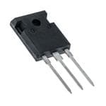
| 产品图片 |
|
| rohs | 符合RoHS无铅 / 符合限制有害物质指令(RoHS)规范要求 |
| 产品系列 | 晶体管,两极晶体管 - BJT,STMicroelectronics BUTW92- |
| 数据手册 | |
| 产品型号 | BUTW92 |
| 不同 Ib、Ic时的 Vce饱和值(最大值) | 1V @ 15A,60A |
| 不同 Ic、Vce 时的DC电流增益(hFE)(最小值) | 9 @ 60A,3V |
| 产品种类 | 两极晶体管 - BJT |
| 供应商器件封装 | TO-247-3 |
| 其它名称 | 497-12117 |
| 其它有关文件 | http://www.st.com/web/catalog/sense_power/FM100/CL822/SC84/PF62912?referrer=70071840 |
| 功率-最大值 | 180W |
| 包装 | 管件 |
| 发射极-基极电压VEBO | 7 V |
| 商标 | STMicroelectronics |
| 安装类型 | 通孔 |
| 安装风格 | Through Hole |
| 封装 | Tube |
| 封装/外壳 | TO-247-3 |
| 封装/箱体 | TO-247 |
| 工厂包装数量 | 30 |
| 晶体管极性 | NPN |
| 晶体管类型 | NPN |
| 最大功率耗散 | 180 W |
| 最大工作温度 | + 150 C |
| 最小工作温度 | - 65 C |
| 标准包装 | 30 |
| 电压-集射极击穿(最大值) | 250V |
| 电流-集电极(Ic)(最大值) | 45A |
| 电流-集电极截止(最大值) | 50µA |
| 直流电流增益hFE最大值 | 65 |
| 直流集电极/BaseGainhfeMin | 9 |
| 系列 | BUTW92 |
| 配置 | Single |
| 集电极—发射极最大电压VCEO | 250 V |
| 集电极—基极电压VCBO | 500 V |
| 集电极—射极饱和电压 | 0.8 V |
| 集电极连续电流 | 60 A |
| 频率-跃迁 | - |


PDF Datasheet 数据手册内容提取
BUTW92 ® HIGH CURRENT NPN SILICON TRANSISTOR n STMicroelectronics PREFERRED SALESTYPE n NPN TRANSISTOR APPLICATIONS: n MOTOR CONTROL n HIGH FREQUENCY AND EFFICIENCY CONVERTERS 3 DESCRIPTION 2 1 High current, high speed transistor suited for power conversion applications, high efficency converters and motor controls. TO-247 INTERNAL SCHEMATIC DIAGRAM ABSOLUTE MAXIMUM RATINGS Symbol Parameter Value Unit VCES Collector-Emitter Voltage (VBE = 0) 500 V VCEO Collector-Emitter Voltage (IB = 0) 250 V VEBO Emitter-Base Voltage (IC = 0) 7 V IE Emitter-Current 60 A IEM Emitter Peak Current (tp < 5ms) 70 A IB Base Current 15 A IBM Base Peak Current (tp < 5ms) 18 A Ptot Total Dissipation at Tc £ 25 oC 180 W Tstg Storage Temperature -65 to 150 oC Tj Max. Operating Junction Temperature 150 oC September 2001 1/4
BUTW92 THERMAL DATA Rthj-case Thermal Resistance Junction-case MAX 0.7 oC/W ELECTRICAL CHARACTERISTICS (Tcase = 25 oC unless otherwise specified) Symbol Parameter Test Conditions Min. Typ. Max. Unit ICES Collector Cut-off VCE = 450 V 50 m A Current (VBE = -1.5V) VCE = 450 V TC = 100oC 1 mA IEBO Emitter Cut-off Current VEB = 5 V 50 m A (IC = 0) VCES Collector-Emitter IC = 5 mA 500 V Voltage (VEB =0) VEBO Emitter-Base Voltage IE = 50 mA 7 V (IC = 0) VCEO(sus)* Collector-Emitter IC = 200 mA 250 V Sustaining Voltage (IB=0) VCE(sat)* Collector-Emitter IC = 60 A IB = 15 A 0.8 1 V Saturation Voltage IC = 60 A IB = 15 A TC = 100oC 1.1 1.5 V VBE(sat)* Base-Emitter IC = 60 A IB = 15 A 1.9 V Saturation Voltage IC = 60 A IB = 15 A TC = 100oC 2 V hFE* DC Current Gain IC = 60 A VCE = 3 V 9 IC = 60 A VCE = 3 V TC = 100oC 6 IC = 5 A VCE = 3 V 65 RESISTIVE LOAD ts Storage Time IC = 50 A VCC = 250 V 1.2 1.4 m s tf Fall Time IB1 = -IB2 = 10 A 250 300 ns * Pulsed: Pulse duration = 300 ms, duty cycle 1.5 % 2/4
BUTW92 TO-247 MECHANICAL DATA mm inch DIM. MIN. TYP. MAX. MIN. TYP. MAX. A 4.7 5.3 0.185 0.209 D 2.2 2.6 0.087 0.102 E 0.4 0.8 0.016 0.031 F 1 1.4 0.039 0.055 F3 2 2.4 0.079 0.094 F4 3 3.4 0.118 0.134 G 10.9 0.429 H 15.3 15.9 0.602 0.626 L 19.7 20.3 0.776 0.779 L3 14.2 14.8 0.559 0.582 L4 34.6 1.362 L5 5.5 0.217 M 2 3 0.079 0.118 P025P 3/4
BUTW92 Information furnished is believed to be accurate and reliable. However, STMicroelectronics assumes no responsibility for the consequences of use of such information nor for any infringement of patents or other rights of third parties which may result from its use. No license is granted by implication or otherwise under any patent or patent rights of STMicroelectronics. Specification mentioned in this publication are subject to change without notice. This publication supersedes and replaces all information previously supplied. STMicroelectronics products are not authorized for use as critical components in life support devices or systems without express written approval of STMicroelectronics. The ST logo is a trademark of STMicroelectronics © 2001 STMicroelectronics – Printed in Italy – All Rights Reserved STMicroelectronics GROUP OF COMPANIES Australia - Brazil - China - Finland - France - Germany - Hong Kong - India - Italy - Japan - Malaysia - Malta - Morocco - Singapore - Spain - Sweden - Switzerland - United Kingdom - U.S.A. http://www.st.com 4/4