ICGOO在线商城 > 集成电路(IC) > PMIC - 配电开关,负载驱动器 > BUK209-50Y,127

 Datasheet下载
- 型号: BUK209-50Y,127
- 制造商: NXP Semiconductors
- 库位|库存: xxxx|xxxx
- 要求:
| 数量阶梯 | 香港交货 | 国内含税 |
| +xxxx | $xxxx | ¥xxxx |
查看当月历史价格
查看今年历史价格
BUK209-50Y,127产品简介:
ICGOO电子元器件商城为您提供BUK209-50Y,127由NXP Semiconductors设计生产,在icgoo商城现货销售,并且可以通过原厂、代理商等渠道进行代购。 BUK209-50Y,127价格参考。NXP SemiconductorsBUK209-50Y,127封装/规格:PMIC - 配电开关,负载驱动器, 。您可以下载BUK209-50Y,127参考资料、Datasheet数据手册功能说明书,资料中有BUK209-50Y,127 详细功能的应用电路图电压和使用方法及教程。
| 参数 | 数值 |
| 产品目录 | 集成电路 (IC) |
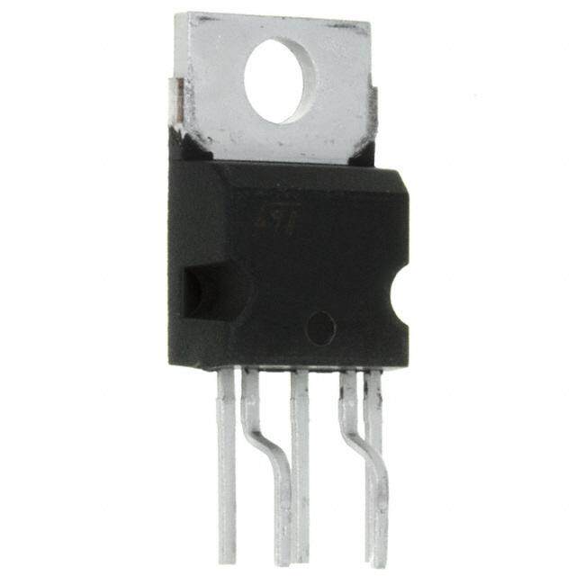
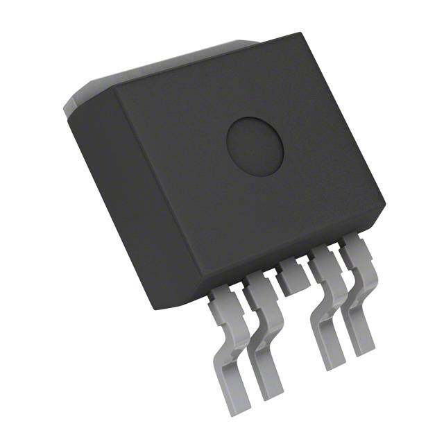
| 描述 | IC TOPFET HIGH SIDE SW TO220-5 |
| 产品分类 | PMIC - MOSFET,电桥驱动器 - 内部开关 |
| 品牌 | NXP Semiconductors |
| 数据手册 | |
| 产品图片 |
|
| 产品型号 | BUK209-50Y,127 |
| rohs | 无铅 / 符合限制有害物质指令(RoHS)规范要求 |
| 产品系列 | TOPFET™ |
| 供应商器件封装 | TO-220-5 |
| 其它名称 | 568-3553-5 |
| 包装 | 管件 |
| 安装类型 | 通孔 |
| 导通电阻 | 45 毫欧 |
| 封装/外壳 | TO-220-5 成形引线 |
| 工作温度 | - |
| 标准包装 | 50 |
| 电压-电源 | 5.5 V ~ 35 V |
| 电流-峰值输出 | 30A |
| 电流-输出/通道 | 12A |
| 类型 | 高端 |
| 输入类型 | 非反相 |
| 输出数 | 1 |
.jpg)


- 商务部:美国ITC正式对集成电路等产品启动337调查
- 曝三星4nm工艺存在良率问题 高通将骁龙8 Gen1或转产台积电
- 太阳诱电将投资9.5亿元在常州建新厂生产MLCC 预计2023年完工
- 英特尔发布欧洲新工厂建设计划 深化IDM 2.0 战略
- 台积电先进制程称霸业界 有大客户加持明年业绩稳了
- 达到5530亿美元!SIA预计今年全球半导体销售额将创下新高
- 英特尔拟将自动驾驶子公司Mobileye上市 估值或超500亿美元
- 三星加码芯片和SET,合并消费电子和移动部门,撤换高东真等 CEO
- 三星电子宣布重大人事变动 还合并消费电子和移动部门
- 海关总署:前11个月进口集成电路产品价值2.52万亿元 增长14.8%


PDF Datasheet 数据手册内容提取
Philips Semiconductors Product specification TOPFET high side switch BUK209-50Y DESCRIPTION QUICK REFERENCE DATA Monolithic single channel high side SYMBOL PARAMETER MIN. UNIT protected power switch in TOPFET2 technology assembled in I Nominal load current (ISO) 6 A L a 5 pin plastic package. APPLICATIONS SYMBOL PARAMETER MAX. UNIT General controller for driving V Continuous off-state supply voltage 50 V BG lamps, motors, solenoids, heaters. I Continuous load current 12 A L T Continuous junction temperature 150 ˚C Rj On-state resistance T = 25˚C 60 mΩ ON j FEATURES FUNCTIONAL BLOCK DIAGRAM Vertical power TrenchMOS Low on-state resistance CMOS logic compatible BATT Very low quiescent current Overtemperature protection STATUS Load current limiting Latched overload and POWER short circuit protection MOSFET Overvoltage and undervoltage INPUT CONTROL & shutdown with hysteresis On-state open circuit load PROTECTION detection Diagnostic status indication CIRCUITS Voltage clamping for turn off of inductive loads ESD protection on all pins LOAD Reverse battery, overvoltage and transient protection GROUND RG Fig.1. Elements of the TOPFET HSS with internal ground resistor. PINNING - SOT263B-01 PIN CONFIGURATION SYMBOL PIN DESCRIPTION mb mb 1 Ground B 2 Input I TOPFET L 3 Battery (+ve supply) HSS S G 4 Status 12345 5 Load Front view MBL267 Fig. 2. Fig. 3. tab connected to pin 3 September 2002 1 Rev 2.000
Philips Semiconductors Product specification TOPFET high side switch BUK209-50Y LIMITING VALUES Limiting values in accordance with the Absolute Maximum System (IEC 134) SYMBOL PARAMETER CONDITIONS MIN. MAX. UNIT V Continuous supply voltage 0 50 V BG I Continuous load current T ≤112˚C - 12 A L mb P Total power dissipation T ≤25˚C - 56 W D mb T Storage temperature -55 175 ˚C stg T Continuous junction temperature1 - 150 ˚C j T Mounting base temperature during soldering - 260 ˚C sold Reverse battery voltages2 -V Continuous reverse voltage - 16 V BG -V Peak reverse voltage - 32 V BG Application information R, R External resistors3 to limit input, status currents 3.2 - kΩ I S Input and status I, I Continuous currents -5 5 mA I S I, I Repetitive peak currents δ ≤ 0.1, tp = 300 µs -50 50 mA I S Inductive load clamping I = 5 A L E Non-repetitive clamping energy T = 150˚C prior to turn-off - 100 mJ BL j ESD LIMITING VALUE SYMBOL PARAMETER CONDITIONS MIN. MAX. UNIT V Electrostatic discharge capacitor Human body model; - 2 kV C voltage C = 250 pF; R = 1.5 kΩ THERMAL CHARACTERISTICS SYMBOL PARAMETER CONDITIONS MIN. TYP. MAX. UNIT Thermal resistance4 R Junction to mounting base - - 1.8 2.2 K/W th j-mb R Junction to ambient in free air - 60 75 K/W th j-a 1 For normal continuous operation. A higher T is allowed as an overload condition but at the threshold T the over temperature trip operates j j(TO) to protect the switch. 2 Reverse battery voltage is allowed only with external resistors to limit the input and status currents to a safe value. The connected load must limit the reverse load current. The internal ground resistor limits the reverse battery ground current. Power is dissipated and the T j rating must be observed. 3 To limit currents during reverse battery and transient overvoltages (positive or negative). 4 Of the output power MOS transistor. September 2002 2 Rev 2.000
Philips Semiconductors Product specification TOPFET high side switch BUK209-50Y STATIC CHARACTERISTICS Limits are at -40˚C ≤ T ≤ 150˚C and typicals at T = 25 ˚C unless otherwise stated. mb mb SYMBOL PARAMETER CONDITIONS MIN. TYP. MAX. UNIT Clamping voltages V Battery to ground I = 1 mA 50 55 65 V BG G V Battery to load I = I = 1 mA 50 55 65 V BL L G -V Negative load to ground I = 10 mA 18 23 28 V LG L -V Negative load voltage1 I = 5 A; t = 300 µs 20 25 30 V LG L p Supply voltage battery to ground V Operating range2 5.5 - 35 V BG Currents 9 V ≤ V ≤ 16 V BG I Quiescent current3 V = 0 V - - 20 µA B LG T = 25˚C - 0.1 2 µA mb I Off-state load current4 V = V - - 20 µA L BL BG T = 25˚C - 0.1 1 µA mb I Operating current5 I = 0 A - 2 4 mA G L I Nominal load current6 V = 0.5 V T = 85˚C 6 - - A L BL mb Resistances V I t 7 T BG L p mb R On-state resistance 9 to 35 V 5 A 300 µs 25˚C - 45 60 mΩ ON 150˚C - - 120 mΩ R On-state resistance 6 V 5 A 300 µs 25˚C - 55 75 mΩ ON 150˚C - - 150 mΩ R Internal ground resistance I = 10 mA 95 150 190 Ω G G 1 For a high side switch, the load pin voltage goes negative with respect to ground during the turn-off of an inductive load. 2 On-state resistance is increased if the supply voltage is less than 9 V. Refer to figure 8. 3 This is the continuous current drawn from the supply when the input is low and includes leakage current to the load. 4 The measured current is in the load pin only. 5 This is the continuous current drawn from the supply with no load connected, but with the input high. 6 Defined as in ISO 10483-1. For comparison purposes only. This parameter will not be characterised for automotive PPAP. 7 The supply and input voltage for the R tests are continuous. The specified pulse duration t refers only to the applied load current. ON p September 2002 3 Rev 2.000
Philips Semiconductors Product specification TOPFET high side switch BUK209-50Y INPUT CHARACTERISTICS 9 V ≤ V ≤ 16 V. Limits are at -40˚C ≤ T ≤ 150˚C and typicals at T = 25 ˚C unless otherwise stated. BG mb mb SYMBOL PARAMETER CONDITIONS MIN. TYP. MAX. UNIT I Input current V = 5 V 20 90 160 µA I IG V Input clamping voltage I = 200 µA 5.5 7 8.5 V IG I V Input turn-on threshold voltage - 2.4 3 V IG(ON) V Input turn-off threshold voltage 1.5 2.1 - V IG(OFF) ∆V Input turn-on hysteresis - 0.3 - V IG I Input turn-on current V = 3 V - - 100 µA I(ON) IG I Input turn-off current V = 1.5 V 10 - - µA I(OFF) IG STATUS CHARACTERISTICS The status output is an open drain transistor, and requires an external pull-up circuit to indicate a logic high. Limits are at -40˚C ≤ T ≤ 150˚C and typicals at T = 25 ˚C unless otherwise stated. Refer to TRUTH TABLE. mb mb SYMBOL PARAMETER CONDITIONS MIN. TYP. MAX. UNIT V Status clamping voltage I = 100 µA 5.5 7 8.5 V SG S V Status low voltage I = 100 µA - - 1 V SG S T = 25˚C - 0.7 0.8 V mb I Status leakage current V = 5 V - - 15 µA S SG T = 25˚C - 0.1 1 µA mb I Status saturation current1 V = 5 V 2 7 12 mA S SG Application information R External pull-up resistor - 47 - kΩ S OPEN CIRCUIT DETECTION CHARACTERISTICS An open circuit load can be detected in the on-state. Refer to TRUTH TABLE. Limits are at -40˚C ≤ T ≤ 150˚C and typical is at T = 25 ˚C. mb mb SYMBOL PARAMETER CONDITIONS MIN. TYP. MAX. UNIT Open circuit detection 9 V ≤ V ≤ 35 V BG I Low current detect threshold 150 - 1000 mA L(TO) T = 25˚C 250 500 750 mA j ∆I Hysteresis - 100 - mA L(TO) 1 In a fault condition with the pull-up resistor short circuited while the status transistor is conducting. This condition should be avoided in order to prevent possible interference with normal operation of the device. September 2002 4 Rev 2.000
Philips Semiconductors Product specification TOPFET high side switch BUK209-50Y UNDERVOLTAGE & OVERVOLTAGE CHARACTERISTICS Limits are at -40˚C ≤ T ≤ 150˚C and typicals at T = 25 ˚C. Refer to TRUTH TABLE. mb mb SYMBOL PARAMETER CONDITIONS MIN. TYP. MAX. UNIT Undervoltage V Low supply threshold voltage1 2 4.2 5.5 V BG(UV) ∆V Hysteresis - 0.5 - V BG(UV) Overvoltage V High supply threshold voltage2 40 45 50 V BG(OV) ∆V Hysteresis - 1 - V BG(OV) TRUTH TABLE ABNORMAL CONDITIONS DETECTED LOAD INPUT SUPPLY LOAD OUTPUT STATUS DESCRIPTION UV OV LC SC OT L X X X X X OFF H off H 0 0 0 0 0 ON H on & normal H 0 0 1 0 0 ON L on & low current detect H 1 0 X X X OFF H supply undervoltage lockout H 0 1 X 0 0 OFF H supply overvoltage shutdown H 0 0 0 1 X OFF L SC tripped H 0 0 0 0 1 OFF L OT shutdown3 KEY TO ABBREVIATIONS L logic low UV undervoltage H logic high OV overvoltage X don’t care LC low current or open circuit load 0 condition not present SC short circuit 1 condition present OT overtemperature 1 Undervoltage sensor causes the device to switch off and reset. 2 Overvoltage sensor causes the device to switch off to protect its load. 3 The status will continue to indicate OT (even if the input goes low) until the device cools below the reset threshold. Refer to OVERLOAD PROTECTION CHARACTERISTICS. September 2002 5 Rev 2.000
Philips Semiconductors Product specification TOPFET high side switch BUK209-50Y OVERLOAD PROTECTION CHARACTERISTICS 5.5 V ≤ V ≤ 35 V, limits are at -40˚C ≤ T ≤ 150˚C and typicals at T = 25 ˚C unless otherwise stated. BG mb mb Refer to TRUTH TABLE. SYMBOL PARAMETER CONDITIONS MIN. TYP. MAX. UNIT Overload protection V = V BL BG I Load current limiting V ≥ 9 V 20 30 40 A L(lim) BG Short circuit load protection V Battery load threshold voltage1 V = 16 V 8 10 12 V BL(TO) BG V = 35 V 15 20 25 V BG t Response time2 V > V - 180 250 µs d sc BL BL(TO) Overtemperature protection T Threshold junction 150 170 190 ˚C j(TO) temperature3 ∆T Hysteresis - 10 - ˚C j(TO) SWITCHING CHARACTERISTICS T = 25 ˚C, V = 13 V, for resistive load R = 13 Ω. mb BG L SYMBOL PARAMETER CONDITIONS MIN. TYP. MAX. UNIT During turn-on from input going high t Delay time to 10% V - 45 70 µs d on L dV/dt Rate of rise of load voltage 30% to 70% V - 0.4 1.0 V/µs on L t Total switching time to 90% V - 110 180 µs on L During turn-off from input going low t Delay time to 90% V - 50 80 µs d off L dV/dt Rate of fall of load voltage 70% to 30% V - 0.7 1.1 V/µs off L t Total switching time to 10% V - 75 120 µs off L CAPACITANCES T = 25 ˚C; f = 1 MHz; V = 0 V. designed in parameters. mb IG SYMBOL PARAMETER CONDITIONS MIN. TYP. MAX. UNIT C Input capacitance V = 13 V - 15 20 pF ig BG C Output capacitance V = 13 V - 200 300 pF bl BL C Status capacitance V = 5 V - 11 15 pF sg SG 1 The battery to load threshold voltage for short circuit protection is proportional to the battery supply voltage. A graph showing V versus BL(TO) V will be provided in the product specification. After short circuit protection has operated, the input voltage must be toggled low for the BG switch to resume normal operation. 2 Measured from when the input goes high. 3 After cooling below the reset temperature the switch will resume normal operation. September 2002 6 Rev 2.000
Philips Semiconductors Product specification TOPFET high side switch BUK209-50Y MECHANICAL DATA Plastic single-ended package; heatsink mounted; 1 mounting hole; 5-lead TO-220 lead form option SOT263B-01 E p1 A ∅ p A1 q D1 mounting D base L3 R L1 L L4 m L2 R 1 5 e b w M Q c Q1 Q2 0 5 10 mm scale DIMENSIONS (mm are the original dimensions) UNIT A A1 b c D D1 E e L L1 L2 L3(1) mL4a(x2). m ∅ p p1 q Q Q1 Q2 R w 4.5 1.39 0.85 0.7 15.8 6.4 10.3 9.8 5.9 5.2 2.4 0.8 3.8 4.3 3.0 mm 1.7 0.5 2.0 4.5 8.2 0.5 0.4 4.1 1.27 0.70 0.4 15.2 5.9 9.7 9.7 5.3 5.0 1.6 0.6 3.6 4.1 2.7 Notes 1. Terminal dimensions are uncontrolled in this zone. 2. Positional accuracy of the terminals is controlled in this zone. OUTLINE REFERENCES EUROPEAN ISSUE DATE VERSION IEC JEDEC EIAJ PROJECTION SOT263B-01 5-lead (option) 01-01-11 TO-220 Fig.4. SOT263B package1 leadform 263B-01, pin 3 connected to mounting base. 1 Refer to mounting instructions for TO220 envelopes. Epoxy meets UL94 VO at 1/8". Net mass: 2 g September 2002 7 Rev 2.000
Philips Semiconductors Product specification TOPFET high side switch BUK209-50Y DEFINITIONS DATA SHEET STATUS DATA SHEET PRODUCT DEFINITIONS STATUS1 STATUS2 Objective data Development This data sheet contains data from the objective specification for product development. Philips Semiconductors reserves the right to change the specification in any manner without notice Preliminary data Qualification This data sheet contains data from the preliminary specification. Supplementary data will be published at a later date. Philips Semiconductors reserves the right to change the specification without notice, in order to improve the design and supply the best possible product Product data Production This data sheet contains data from the product specification. Philips Semiconductors reserves the right to make changes at any time in order to improve the design, manufacturing and supply. Changes will be communicated according to the Customer Product/Process Change Notification (CPCN) procedure SNW-SQ-650A Limiting values Limiting values are given in accordance with the Absolute Maximum Rating System (IEC 134). Stress above one or more of the limiting values may cause permanent damage to the device. These are stress ratings only and operation of the device at these or at any other conditions above those given in the Characteristics sections of this specification is not implied. Exposure to limiting values for extended periods may affect device reliability. Application information Where application information is given, it is advisory and does not form part of the specification. Philips Electronics N.V. 2002 All rights are reserved. Reproduction in whole or in part is prohibited without the prior written consent of the copyright owner. The information presented in this document does not form part of any quotation or contract, it is believed to be accurate and reliable and may be changed without notice. No liability will be accepted by the publisher for any consequence of its use. Publication thereof does not convey nor imply any license under patent or other industrial or intellectual property rights. LIFE SUPPORT APPLICATIONS These products are not designed for use in life support appliances, devices or systems where malfunction of these products can be reasonably expected to result in personal injury. Philips customers using or selling these products for use in such applications do so at their own risk and agree to fully indemnify Philips for any damages resulting from such improper use or sale. 1 Please consult the most recently issued datasheet before initiating or completing a design. 2 The product status of the device(s) described in this datasheet may have changed since this datasheet was published. The latest information is available on the Internet at URL http://www.semiconductors.philips.com. September 2002 8 Rev 2.000