ICGOO在线商城 > BTS716GB
 Datasheet下载
- 型号: BTS716GB
- 制造商: Infineon
- 库位|库存: xxxx|xxxx
- 要求:
| 数量阶梯 | 香港交货 | 国内含税 |
| +xxxx | $xxxx | ¥xxxx |
查看当月历史价格
查看今年历史价格
BTS716GB产品简介:
ICGOO电子元器件商城为您提供BTS716GB由Infineon设计生产,在icgoo商城现货销售,并且可以通过原厂、代理商等渠道进行代购。 提供BTS716GB价格参考以及InfineonBTS716GB封装/规格参数等产品信息。 你可以下载BTS716GB参考资料、Datasheet数据手册功能说明书, 资料中有BTS716GB详细功能的应用电路图电压和使用方法及教程。
| 参数 | 数值 |
| 产品目录 | 集成电路 (IC)半导体 |
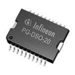
| 描述 | IC HISIDE PWR SWITCH 4CH PDSO-20电源开关 IC - POE / LAN SMART HI SIDE PWR SWITCH INDUSTRY APP |
| 产品分类 | PMIC - MOSFET,电桥驱动器 - 内部开关集成电路 - IC |
| 品牌 | Infineon Technologies |
| 产品手册 | http://www.infineon.com/dgdl/BTS716GB_2007_GDS10.pdf?folderId=db3a304314dca389011537739e37155f&fileId=db3a30431c48a312011c4c2a11d90028 |
| 产品图片 |
|
| rohs | 符合RoHS无铅 / 符合限制有害物质指令(RoHS)规范要求 |
| 产品系列 | 开关 IC,电源开关 IC - POE / LAN,Infineon Technologies BTS716GB- |
| 数据手册 | http://www.infineon.com/dgdl/BTS716GB_2007_GDS10.pdf?folderId=db3a304314dca389011537739e37155f&fileId=db3a30431c48a312011c4c2a11d90028 |
| 产品型号 | BTS716GB |
| 产品目录页面 | |
| 产品种类 | 电源开关 IC - POE / LAN |
| 供应商器件封装 | PG-DSO-20 |
| 其它名称 | BTS716GBDKR |
| 包装 | Digi-Reel® |
| 商标 | Infineon Technologies |
| 安装类型 | 表面贴装 |
| 安装风格 | SMD/SMT |
| 导通电阻 | 110 毫欧 |
| 导通电阻—最大值 | 0.11 Ohms |
| 封装 | Reel |
| 封装/外壳 | 20-SOIC(0.295",7.50mm 宽) |
| 封装/箱体 | DSO-20 |
| 工作温度 | -40°C ~ 150°C |
| 工厂包装数量 | 1000 |
| 最大功率耗散 | 3600 mW |
| 最大工作温度 | + 150 C |
| 最小工作温度 | - 40 C |
| 标准包装 | 1 |
| 电压-电源 | 5.5 V ~ 40 V |
| 电流-峰值输出 | 6.5A |
| 电流-输出/通道 | 2.6A |
| 类型 | 高端 |
| 系列 | BTS716 |
| 输入类型 | 非反相 |
| 输出数 | 4 |
| 零件号别名 | BTS716GBXUMA1 SP000272337 |


- 商务部:美国ITC正式对集成电路等产品启动337调查
- 曝三星4nm工艺存在良率问题 高通将骁龙8 Gen1或转产台积电
- 太阳诱电将投资9.5亿元在常州建新厂生产MLCC 预计2023年完工
- 英特尔发布欧洲新工厂建设计划 深化IDM 2.0 战略
- 台积电先进制程称霸业界 有大客户加持明年业绩稳了
- 达到5530亿美元!SIA预计今年全球半导体销售额将创下新高
- 英特尔拟将自动驾驶子公司Mobileye上市 估值或超500亿美元
- 三星加码芯片和SET,合并消费电子和移动部门,撤换高东真等 CEO
- 三星电子宣布重大人事变动 还合并消费电子和移动部门
- 海关总署:前11个月进口集成电路产品价值2.52万亿元 增长14.8%


PDF Datasheet 数据手册内容提取
Smart High-Side Power Switch BTS716GB (cid:1)(cid:2)(cid:3)(cid:4)(cid:5)(cid:6)(cid:7)(cid:8)(cid:9)(cid:10)(cid:11)(cid:1)(cid:8)(cid:12)(cid:13)(cid:6)(cid:14)(cid:15)(cid:16)(cid:13)(cid:4)(cid:6)(cid:1)(cid:16)(cid:8)(cid:5)(cid:17)(cid:10)(cid:6) (cid:18)(cid:15)(cid:19)(cid:4)(cid:6)(cid:20)(cid:10)(cid:3)(cid:21)(cid:21)(cid:13)(cid:22)(cid:23)(cid:24)(cid:6)(cid:25)(cid:6)(cid:26)(cid:6)(cid:27)(cid:25)(cid:28)(cid:2)Ω(cid:6) (cid:1)(cid:5)(cid:3)(cid:5)(cid:19)(cid:23)(cid:6)(cid:18)(cid:13)(cid:13)(cid:12)(cid:29)(cid:3)(cid:17)(cid:30)(cid:6) Product Summary Package (cid:1)(cid:2)(cid:3)(cid:4)(cid:5)(cid:6)(cid:7)(cid:8)(cid:9)(cid:10)(cid:11)(cid:12)(cid:13)(cid:6)(cid:5)(cid:9)(cid:3)(cid:10) (cid:11) (cid:10) (cid:15)(cid:16)(cid:15)(cid:10)(cid:16)(cid:16)(cid:16)(cid:17)(cid:18)(cid:11)(cid:10) (cid:14)(cid:14) P-DSO-20 (cid:19)(cid:20)(cid:6)(cid:7)(cid:21)(cid:3)(cid:10)(cid:20)(cid:22)(cid:5)(cid:8)(cid:8)(cid:3)(cid:13)(cid:23)(cid:10) (cid:12)(cid:8)(cid:3)(cid:10) (cid:24)(cid:12)(cid:25)(cid:4)(cid:10)(cid:2)(cid:5)(cid:4)(cid:5)(cid:13)(cid:13)(cid:3)(cid:13)(cid:10) (cid:1)(cid:8)(cid:26)(cid:23)(cid:6)(cid:5)(cid:6)(cid:3)(cid:10)(cid:27)(cid:3)(cid:23)(cid:7)(cid:23)(cid:6)(cid:5)(cid:8)(cid:20)(cid:3)(cid:10) (cid:27) (cid:10) (cid:29)(cid:17)(cid:18)(cid:30)Ω(cid:10) (cid:31)(cid:15)(cid:30)Ω(cid:10) (cid:1)(cid:28) (cid:28)(cid:12)(cid:30)(cid:7)(cid:8)(cid:5)(cid:13)(cid:10)(cid:13)(cid:12)(cid:5) (cid:10)(cid:20)(cid:25)(cid:4)(cid:4)(cid:3)(cid:8)(cid:6)(cid:10) ! (cid:10) &(cid:16)’(cid:19)(cid:10) (cid:15)(cid:16)(cid:31)(cid:19)(cid:10) "#(cid:28)(cid:1)$% ((cid:25)(cid:4)(cid:4)(cid:3)(cid:8)(cid:6)(cid:10)(cid:13)(cid:7)(cid:30)(cid:7)(cid:6)(cid:5)(cid:6)(cid:7)(cid:12)(cid:8)(cid:10) ! (cid:10) ’(cid:16)(cid:15)(cid:19)(cid:10) ’(cid:16)(cid:15)(cid:19)(cid:10) "#)((cid:4)% PG-DSO20 (cid:31)(cid:13)(cid:21)(cid:13)(cid:4)(cid:3)(cid:22)(cid:6) (cid:13)(cid:23)(cid:17)(cid:4)(cid:8)!(cid:5)(cid:8)(cid:15)(cid:21)(cid:6) •(cid:10) (cid:28)(cid:10)(cid:20)(cid:22)(cid:5)(cid:8)(cid:8)(cid:3)(cid:13)(cid:10)(cid:21)(cid:3)(cid:4)(cid:6)(cid:7)(cid:20)(cid:5)(cid:13)(cid:10)(cid:2)(cid:12)*(cid:3)(cid:4)(cid:10)$(cid:1))+,-(cid:10)*(cid:7)(cid:6)(cid:22)(cid:10)(cid:20)(cid:22)(cid:5)(cid:4)(cid:9)(cid:3)(cid:10)(cid:2)(cid:25)(cid:30)(cid:2).(cid:10)(cid:9)(cid:4)(cid:12)(cid:25)(cid:8) (cid:10)(cid:4)(cid:3)(cid:24)(cid:3)(cid:4)(cid:3)(cid:8)(cid:20)(cid:3) (cid:10)($(cid:1))(cid:10)(cid:20)(cid:12)(cid:30)(cid:2)(cid:5)(cid:6)(cid:7)(cid:14)(cid:13)(cid:3)(cid:10)(cid:7)(cid:8)(cid:2)(cid:25)(cid:6)(cid:10)(cid:5)(cid:8) (cid:10) (cid:7)(cid:5)(cid:9)(cid:8)(cid:12)(cid:23)(cid:6)(cid:7)(cid:20)(cid:10)(cid:24)(cid:3)(cid:3) (cid:14)(cid:5)(cid:20)/.(cid:10)(cid:30)(cid:12)(cid:8)(cid:12)(cid:13)(cid:7)(cid:6)(cid:22)(cid:7)(cid:20)(cid:5)(cid:13)(cid:13)0(cid:10)(cid:7)(cid:8)(cid:6)(cid:3)(cid:9)(cid:4)(cid:5)(cid:6)(cid:3) (cid:10)(cid:7)(cid:8)(cid:10))(cid:30)(cid:5)(cid:4)(cid:6)(cid:10))!1$(cid:1))(cid:10)(cid:6)(cid:3)(cid:20)(cid:22)(cid:8)(cid:12)(cid:13)(cid:12)(cid:9)0(cid:16)(cid:10) •(cid:10) +(cid:25)(cid:13)(cid:13)0(cid:10)(cid:2)(cid:4)(cid:12)(cid:6)(cid:3)(cid:20)(cid:6)(cid:3) (cid:10)(cid:14)0(cid:10)(cid:3)(cid:30)(cid:14)(cid:3) (cid:3) (cid:10)(cid:2)(cid:4)(cid:12)(cid:6)(cid:3)(cid:20)(cid:6)(cid:7)(cid:12)(cid:8)(cid:10)(cid:24)(cid:25)(cid:8)(cid:20)(cid:6)(cid:7)(cid:12)(cid:8)(cid:23)(cid:10) "!!(cid:22)(cid:8)(cid:17)(cid:3)(cid:5)(cid:8)(cid:15)(cid:21)(cid:23)(cid:6) •(cid:10) 2((cid:10)(cid:20)(cid:12)(cid:30)(cid:2)(cid:5)(cid:6)(cid:7)(cid:14)(cid:13)(cid:3)(cid:10)(cid:22)(cid:7)(cid:9)(cid:22)(cid:26)(cid:23)(cid:7) (cid:3)(cid:10)(cid:2)(cid:12)*(cid:3)(cid:4)(cid:10)(cid:23)*(cid:7)(cid:6)(cid:20)(cid:22)(cid:10)*(cid:7)(cid:6)(cid:22)(cid:10) (cid:7)(cid:5)(cid:9)(cid:8)(cid:12)(cid:23)(cid:6)(cid:7)(cid:20)(cid:10)(cid:24)(cid:3)(cid:3) (cid:14)(cid:5)(cid:20)/(cid:10)(cid:24)(cid:12)(cid:4)(cid:10)(cid:29)&(cid:11)(cid:10)(cid:5)(cid:8) (cid:10)&(cid:17)(cid:11)(cid:10)(cid:9)(cid:4)(cid:12)(cid:25)(cid:8) (cid:3) (cid:10)(cid:13)(cid:12)(cid:5) (cid:23)(cid:10) •(cid:10) (cid:19)(cid:13)(cid:13)(cid:10)(cid:6)0(cid:2)(cid:3)(cid:23)(cid:10)(cid:12)(cid:24)(cid:10)(cid:4)(cid:3)(cid:23)(cid:7)(cid:23)(cid:6)(cid:7)(cid:21)(cid:3).(cid:10)(cid:7)(cid:8) (cid:25)(cid:20)(cid:6)(cid:7)(cid:21)(cid:3)(cid:10)(cid:5)(cid:8) (cid:10)(cid:20)(cid:5)(cid:2)(cid:5)(cid:20)(cid:7)(cid:6)(cid:21)(cid:3)(cid:10)(cid:13)(cid:12)(cid:5) (cid:23)(cid:10) •(cid:10) $(cid:12)(cid:23)(cid:6)(cid:10)(cid:23)(cid:25)(cid:7)(cid:6)(cid:5)(cid:14)(cid:13)(cid:3)(cid:10)(cid:24)(cid:12)(cid:4)(cid:10)(cid:13)(cid:12)(cid:5) (cid:23)(cid:10)*(cid:7)(cid:6)(cid:22)(cid:10)(cid:22)(cid:7)(cid:9)(cid:22)(cid:10)(cid:7)(cid:8)(cid:4)(cid:25)(cid:23)(cid:22)(cid:10)(cid:20)(cid:25)(cid:4)(cid:4)(cid:3)(cid:8)(cid:6)(cid:23).(cid:10)(cid:23)(cid:12)(cid:10)(cid:5)(cid:23)(cid:10)(cid:13)(cid:5)(cid:30)(cid:2)(cid:23)(cid:10) •(cid:10) (cid:27)(cid:3)(cid:2)(cid:13)(cid:5)(cid:20)(cid:3)(cid:23)(cid:10)(cid:3)(cid:13)(cid:3)(cid:20)(cid:6)(cid:4)(cid:12)(cid:30)(cid:3)(cid:20)(cid:22)(cid:5)(cid:8)(cid:7)(cid:20)(cid:5)(cid:13)(cid:10)(cid:4)(cid:3)(cid:13)(cid:5)0(cid:23).(cid:10)(cid:24)(cid:25)(cid:23)(cid:3)(cid:23)(cid:10)(cid:5)(cid:8) (cid:10) (cid:7)(cid:23)(cid:20)(cid:4)(cid:3)(cid:6)(cid:3)(cid:10)(cid:20)(cid:7)(cid:4)(cid:20)(cid:25)(cid:7)(cid:6)(cid:23)(cid:10) #(cid:3)(cid:23)(cid:8)(cid:17)(cid:6)(cid:18)(cid:19)(cid:21)(cid:17)(cid:5)(cid:8)(cid:15)(cid:21)(cid:23)(cid:6) •(cid:10) (cid:11)(cid:3)(cid:4)0(cid:10)(cid:13)(cid:12)*(cid:10)(cid:23)(cid:6)(cid:5)(cid:8) (cid:14)0(cid:10)(cid:20)(cid:25)(cid:4)(cid:4)(cid:3)(cid:8)(cid:6)(cid:10) •(cid:10) ($(cid:1))(cid:10)(cid:20)(cid:12)(cid:30)(cid:2)(cid:5)(cid:6)(cid:7)(cid:14)(cid:13)(cid:3)(cid:10)(cid:7)(cid:8)(cid:2)(cid:25)(cid:6)(cid:10) •(cid:10) !(cid:30)(cid:2)(cid:4)(cid:12)(cid:21)(cid:3) (cid:10)(cid:3)(cid:13)(cid:3)(cid:20)(cid:6)(cid:4)(cid:12)(cid:30)(cid:5)(cid:9)(cid:8)(cid:3)(cid:6)(cid:7)(cid:20)(cid:10)(cid:20)(cid:12)(cid:30)(cid:2)(cid:5)(cid:6)(cid:7)(cid:14)(cid:7)(cid:13)(cid:7)(cid:6)0(cid:10)#,$(%(cid:10) •(cid:10) +(cid:5)(cid:23)(cid:6)(cid:10) (cid:3)(cid:30)(cid:5)(cid:9)(cid:8)(cid:3)(cid:6)(cid:7)3(cid:5)(cid:6)(cid:7)(cid:12)(cid:8)(cid:10)(cid:12)(cid:24)(cid:10)(cid:7)(cid:8) (cid:25)(cid:20)(cid:6)(cid:7)(cid:21)(cid:3)(cid:10)(cid:13)(cid:12)(cid:5) (cid:23)(cid:10) •(cid:10) )(cid:6)(cid:5)(cid:14)(cid:13)(cid:3)(cid:10)(cid:14)(cid:3)(cid:22)(cid:5)(cid:21)(cid:7)(cid:12)(cid:25)(cid:4)(cid:10)(cid:5)(cid:6)(cid:10)(cid:25)(cid:8) (cid:3)(cid:4)(cid:21)(cid:12)(cid:13)(cid:6)(cid:5)(cid:9)(cid:3)(cid:10) •(cid:10) 4(cid:7) (cid:3)(cid:10)(cid:12)(cid:2)(cid:3)(cid:4)(cid:5)(cid:6)(cid:7)(cid:8)(cid:9)(cid:10)(cid:21)(cid:12)(cid:13)(cid:6)(cid:5)(cid:9)(cid:3)(cid:10)(cid:4)(cid:5)(cid:8)(cid:9)(cid:3)(cid:10) •(cid:10) "(cid:12)(cid:9)(cid:7)(cid:20)(cid:10)(cid:9)(cid:4)(cid:12)(cid:25)(cid:8) (cid:10)(cid:7)(cid:8) (cid:3)(cid:2)(cid:3)(cid:8) (cid:3)(cid:8)(cid:6)(cid:10)(cid:24)(cid:4)(cid:12)(cid:30)(cid:10)(cid:13)(cid:12)(cid:5) (cid:10)(cid:9)(cid:4)(cid:12)(cid:25)(cid:8) (cid:10) (cid:14)(cid:4)(cid:15)(cid:5)(cid:13)(cid:17)(cid:5)(cid:8)(cid:15)(cid:21)(cid:6)(cid:18)(cid:19)(cid:21)(cid:17)(cid:5)(cid:8)(cid:15)(cid:21)(cid:23)(cid:6) (cid:6) (cid:6) (cid:6) (cid:6) Block Diagram(cid:6) •(cid:10) )(cid:22)(cid:12)(cid:4)(cid:6)(cid:10)(cid:20)(cid:7)(cid:4)(cid:20)(cid:25)(cid:7)(cid:6)(cid:10)(cid:2)(cid:4)(cid:12)(cid:6)(cid:3)(cid:20)(cid:6)(cid:7)(cid:12)(cid:8)(cid:10) •(cid:10) (cid:1)(cid:21)(cid:3)(cid:4)(cid:13)(cid:12)(cid:5) (cid:10)(cid:2)(cid:4)(cid:12)(cid:6)(cid:3)(cid:20)(cid:6)(cid:7)(cid:12)(cid:8)(cid:10)(cid:10) (cid:11)(cid:14)(cid:14) •(cid:10) ((cid:25)(cid:4)(cid:4)(cid:3)(cid:8)(cid:6)(cid:10)(cid:13)(cid:7)(cid:30)(cid:7)(cid:6)(cid:5)(cid:6)(cid:7)(cid:12)(cid:8)(cid:10) •(cid:10) -(cid:22)(cid:3)(cid:4)(cid:30)(cid:5)(cid:13)(cid:10)(cid:23)(cid:22)(cid:25)(cid:6) (cid:12)*(cid:8)(cid:10) ’((cid:27) $(cid:15)(cid:9)(cid:8)(cid:17) •(cid:10) (cid:1)(cid:21)(cid:3)(cid:4)(cid:21)(cid:12)(cid:13)(cid:6)(cid:5)(cid:9)(cid:3)(cid:10)(cid:2)(cid:4)(cid:12)(cid:6)(cid:3)(cid:20)(cid:6)(cid:7)(cid:12)(cid:8)(cid:10)#(cid:7)(cid:8)(cid:20)(cid:13)(cid:25) (cid:7)(cid:8)(cid:9)(cid:10)(cid:13)(cid:12)(cid:5) (cid:10) (cid:25)(cid:30)(cid:2)%(cid:10)*(cid:7)(cid:6)(cid:22)(cid:10)(cid:3)5(cid:6)(cid:3)(cid:4)(cid:8)(cid:5)(cid:13)(cid:10) (cid:1))(cid:27)*& (cid:20)(cid:10)(cid:3)(cid:21)(cid:21)(cid:13)(cid:22)(cid:6)(cid:27) (cid:4)(cid:3)(cid:23)(cid:7)(cid:23)(cid:6)(cid:12)(cid:4)(cid:10) ’(& (cid:20)(cid:10)(cid:3)(cid:21)(cid:21)(cid:13)(cid:22)(cid:6)& $(cid:15)(cid:3)(cid:12)(cid:6)(cid:27) •(cid:10) (cid:27)(cid:3)(cid:21)(cid:3)(cid:4)(cid:23)(cid:3)(cid:10)(cid:14)(cid:5)(cid:6)(cid:6)(cid:3)(cid:4)0(cid:10)(cid:2)(cid:4)(cid:12)(cid:6)(cid:3)(cid:20)(cid:6)(cid:7)(cid:12)(cid:8)(cid:10)*(cid:7)(cid:6)(cid:22)(cid:10)(cid:3)5(cid:6)(cid:3)(cid:4)(cid:8)(cid:5)(cid:13)(cid:10)(cid:4)(cid:3)(cid:23)(cid:7)(cid:23)(cid:6)(cid:12)(cid:4)(cid:10) •(cid:10) "(cid:12)(cid:23)(cid:23)(cid:10)(cid:12)(cid:24)(cid:10)(cid:9)(cid:4)(cid:12)(cid:25)(cid:8) (cid:10)(cid:5)(cid:8) (cid:10)(cid:13)(cid:12)(cid:23)(cid:23)(cid:10)(cid:12)(cid:24)(cid:10)(cid:11) (cid:10)(cid:2)(cid:4)(cid:12)(cid:6)(cid:3)(cid:20)(cid:6)(cid:7)(cid:12)(cid:8)(cid:10) $(cid:15)(cid:3)(cid:12)(cid:6)& (cid:14)(cid:14) •(cid:10) ,(cid:13)(cid:3)(cid:20)(cid:6)(cid:4)(cid:12)(cid:23)(cid:6)(cid:5)(cid:6)(cid:7)(cid:20)(cid:10) (cid:7)(cid:23)(cid:20)(cid:22)(cid:5)(cid:4)(cid:9)(cid:3)(cid:10)(cid:2)(cid:4)(cid:12)(cid:6)(cid:3)(cid:20)(cid:6)(cid:7)(cid:12)(cid:8)(cid:10)#,)6%(cid:10) ’(% $(cid:15)(cid:9)(cid:8)(cid:17) (cid:1))%*(cid:25) (cid:20)(cid:10)(cid:3)(cid:21)(cid:21)(cid:13)(cid:22)(cid:6)% (cid:8)(cid:3)(cid:9)(cid:21)(cid:15)(cid:23)(cid:5)(cid:8)(cid:17)(cid:6)(cid:18)(cid:19)(cid:21)(cid:17)(cid:5)(cid:8)(cid:15)(cid:21)(cid:6) $(cid:15)(cid:3)(cid:12)(cid:6)% ’((cid:25) (cid:20)(cid:10)(cid:3)(cid:21)(cid:21)(cid:13)(cid:22)(cid:6)(cid:25) •(cid:10) 6(cid:7)(cid:5)(cid:9)(cid:8)(cid:12)(cid:23)(cid:6)(cid:7)(cid:20)(cid:10)(cid:24)(cid:3)(cid:3) (cid:14)(cid:5)(cid:20)/(cid:10)*(cid:7)(cid:6)(cid:22)(cid:10)(cid:12)(cid:2)(cid:3)(cid:8)(cid:10) (cid:4)(cid:5)(cid:7)(cid:8)(cid:10)(cid:12)(cid:25)(cid:6)(cid:2)(cid:25)(cid:6)(cid:10) •(cid:10) (cid:1)(cid:2)(cid:3)(cid:8)(cid:10)(cid:13)(cid:12)(cid:5) (cid:10) (cid:3)(cid:6)(cid:3)(cid:20)(cid:6)(cid:7)(cid:12)(cid:8)(cid:10)(cid:7)(cid:8)(cid:10)(cid:1)++(cid:26)(cid:23)(cid:6)(cid:5)(cid:6)(cid:3)(cid:10) 7(cid:28)6 $(cid:15)(cid:3)(cid:12)(cid:6)(cid:25) •(cid:10) +(cid:3)(cid:3) (cid:14)(cid:5)(cid:20)/(cid:10)(cid:12)(cid:24)(cid:10)(cid:6)(cid:22)(cid:3)(cid:4)(cid:30)(cid:5)(cid:13)(cid:10)(cid:23)(cid:22)(cid:25)(cid:6) (cid:12)*(cid:8)(cid:10)(cid:7)(cid:8)(cid:10)(cid:1)(cid:28)(cid:26)(cid:23)(cid:6)(cid:5)(cid:6)(cid:3)(cid:10) Data Sheet 1 V1.0, 2007-05-13
Smart High-Side Power Switch BTS716GB (cid:18)(cid:19)(cid:21)(cid:17)(cid:5)(cid:8)(cid:15)(cid:21)(cid:3)(cid:22)(cid:6)(cid:12)(cid:8)(cid:3)(cid:9)(cid:4)(cid:3)(cid:2)(cid:6)(cid:6) (cid:10) (cid:10) (cid:10) (cid:10) (cid:12)(cid:21)(cid:3)(cid:4)(cid:21)(cid:12)(cid:13)(cid:6)(cid:5)(cid:9)(cid:3)(cid:10) (cid:10) (cid:2)(cid:4)(cid:12)(cid:6)(cid:3)(cid:20)(cid:6)(cid:7)(cid:12)(cid:8) (cid:10) (cid:9)(cid:5)(cid:6)(cid:3)(cid:10) (cid:20)(cid:25)(cid:4)(cid:4)(cid:3)(cid:8)(cid:6)(cid:10)(cid:13)(cid:7)(cid:30)(cid:7)(cid:6) (cid:11):: (cid:10) (cid:10) (cid:20)(cid:12)(cid:8)(cid:6)(cid:4)(cid:12)(cid:13)(cid:10) (cid:10) (cid:10) 9(cid:10) (cid:10) (cid:7)(cid:8)(cid:6)(cid:3)(cid:4)(cid:8)(cid:5)(cid:13)(cid:10) (cid:10) (cid:20)(cid:22)(cid:5)(cid:4)(cid:9)(cid:3)(cid:10) (cid:10) (cid:20)(cid:13)(cid:5)(cid:30)(cid:2)(cid:10)(cid:24)(cid:12)(cid:4)(cid:10) (cid:21)(cid:12)(cid:13)(cid:6)(cid:5)(cid:9)(cid:3)(cid:10)(cid:23)(cid:25)(cid:2)(cid:2)(cid:13)0(cid:10) (cid:13)(cid:12)(cid:9)(cid:7)(cid:20)(cid:10) (cid:2)(cid:25)(cid:30)(cid:2)(cid:10) (cid:10) (cid:7)(cid:8) (cid:25)(cid:20)(cid:6)(cid:7)(cid:21)(cid:3)(cid:10)(cid:13)(cid:12)(cid:5) (cid:10) (cid:1)8-(cid:29)(cid:10) (cid:10) (cid:10) !(cid:28)(cid:29)(cid:10) (cid:10) (cid:6)(cid:3)(cid:30)(cid:2)(cid:3)(cid:4)(cid:5)(cid:6)(cid:25)(cid:4)(cid:3)(cid:10) (cid:4)(cid:3)(cid:21)(cid:3)(cid:4)(cid:23)(cid:3)(cid:10) (cid:10) (cid:10) (cid:23)(cid:3)(cid:8)(cid:23)(cid:12)(cid:4)(cid:10) (cid:14)(cid:5)(cid:6)(cid:6)(cid:3)(cid:4)0(cid:10) ,)6(cid:10) (cid:10) (cid:2)(cid:4)(cid:12)(cid:6)(cid:3)(cid:20)(cid:6)(cid:7)(cid:12)(cid:8)(cid:10) "(cid:1)(cid:19)6(cid:10) (cid:10) (cid:1)(cid:2)(cid:3)(cid:8)(cid:10)(cid:13)(cid:12)(cid:5) (cid:10)(cid:10) (cid:10) (cid:3)(cid:6)(cid:3)(cid:20)(cid:6)(cid:7)(cid:12)(cid:8)(cid:10) (cid:10) (cid:10) (cid:10) (cid:10)(cid:16)(cid:10)(cid:10) (cid:10) (cid:10) (cid:10) (cid:10)(cid:10)(cid:10)(cid:10)(cid:10)(cid:10)(cid:10)(cid:10)(cid:10)(cid:10)(cid:20)(cid:22)(cid:5)(cid:8)(cid:8)(cid:3)(cid:13)(cid:10)(cid:29)(cid:10) (cid:10) )-(cid:29);&(cid:10) (cid:10) (cid:10) (cid:10) (cid:10) !(cid:28)&(cid:10) control and protection circuit (cid:10) of (cid:10) channel 2 (cid:10) (cid:10) 7(cid:28)6(cid:29);&(cid:10) (cid:1)8-&(cid:10) (cid:10) (cid:10) (cid:10) (cid:10) (cid:10) (cid:10) !(cid:28)(cid:31)(cid:10) control and protection circuit (cid:10) of (cid:10) channel 3 (cid:10) (cid:10) (cid:1)8-(cid:31)(cid:10) (cid:10) (cid:10) )-(cid:31);(cid:17)(cid:10) (cid:10) (cid:10) (cid:10) (cid:10) IN4 control and protection circuit (cid:10) of (cid:10) channel 4 (cid:10) (cid:10) 7(cid:28)6(cid:31);(cid:17)(cid:10) (cid:1)8-(cid:17)(cid:10) (cid:10) (cid:10) (cid:10) (cid:10) (cid:10) (cid:10) (cid:10) (cid:10) Data Sheet 2 V1.0, 2007-05-13
Smart High-Side Power Switch BTS716GB Pin Definitions and Functions Pin configuration Pin Symbol Function (top view) 1,10, V Positive power supply voltage. Design the bb 11,12, wiring for the simultaneous max. short circuit • V 1 20 V 15,16, currents from channel 1 to 2 and also for low bb bb GND1/2 2 19 V 19,20 thermal resistance bb IN1 3 18 OUT1 3 IN1 Input 1,2,3,4 activates channel 1,2,3,4 in case ST1/2 4 17 OUT2 5 IN2 of logic high signal IN2 5 16 V 7 IN3 bb GND3/4 6 15 V 9 IN4 bb 18 OUT1 Output 1,2,3,4 protected high-side power output IN3 7 14 OUT3 17 OUT2 of channel 1,2,3,4. Design the wiring for the ST3/4 8 13 OUT4 14 OUT3 max. short circuit current IN4 9 12 Vbb 13 OUT4 V 10 11 V bb bb 4 ST1/2 Diagnostic feedback 1/2,3/4 of channel 1,2,3,4 8 ST3/4 open drain, low on failure 2 GND1/2 Ground of chip 1 (channel 1,2) 6 GND3/4 Ground of chip 2 (channel 3,4) Data Sheet 3 V1.0, 2007-05-13
Smart High-Side Power Switch BTS716GB Parameter Symbol Values Unit Supply voltage (overvoltage protection see page 6) V 43 V bb Supply voltage for full short circuit protection V 36 V bb T =-40 ...+150°C j,start Load current (Short-circuit current, see page 6) I I 1 A L L(lim) Load dump protection2)VLoadDump = VA + Vs,VA = 13.5 V VLoaddump4) 60 V RI3)= 2Ω,td= 400ms; IN= low or high, each channel loaded with R =13.5 Ω, L Operating temperature range T -40 ...+150 °C j Storage temperature range T -55 ...+150 stg Power dissipation (DC)5) T = 25°C: P 3.6 W a tot (all channels active) T = 85°C: 1.9 a Maximal switchable inductance, single pulse Vbb=12V,Tj,start=150°C5), see diagrams on page 10 I =2.3A,E =76 mJ, 0Ω one channel: Z 21 mH L AS L I =3.3A,E =182 mJ, 0Ω two parallel channels: 25 L AS I =4.7A,E =460 mJ, 0Ω four parallel channels: 30 L AS Electrostatic discharge capability (ESD) IN: V 1.0 kV ESD (Human Body Model) ST: 4.0 out to all other pins shorted: 8.0 acc. MIL-STD883D, method 3015.7 and ESD assn. std. S5.1-1993 R=1.5kΩ; C=100pF Input voltage (DC) see internal circuit diagram page 9 V -10 ... +16 V IN Current through input pin (DC) I ±0.3 mA IN Pulsed current through input pin6) I ±5.0 IN Current through status pin (DC) I ±5.0 ST 1) Operation in current limitation is considered as "outside" normal operating range. Protection functions are not designed for continuous repetitive operation. 2) Supply voltages higher than V require an external current limit for the GND and status pins (a 150Ω bb(AZ) resistor for the GND connection is recommended. 3) R = internal resistance of the load dump test pulse generator I 4) V is setup without the DUT connected to the generator per ISO 7637-1 and DIN 40839 Load dump 5) Device on 50mm*50mm*1.5mm epoxy PCB FR4 with 6cm2 (one layer, 70µm thick) copper area for Vbb connection. PCB is vertical without blown air. See page 14 6) only for testing Data Sheet 4 V1.0, 2007-05-13
Smart High-Side Power Switch BTS716GB Parameter and Conditions Symbol Values Unit min typ max Thermal resistance junction - soldering point7)8) each channel: R -- -- 17 K/W thjs junction – ambient6) R -- -- -- thja @ 6 cm2 cooling area one channel active: -- 44 -- all channels active: -- 35 -- Electrical Characteristics Parameter and Conditions, each of the four channels Symbol Values Unit at Tj = -40...+150°C, Vbb = 12 V unless otherwise specified min typ max Load Switching Capabilities and Characteristics On-state resistance (Vbb to OUT); IL = 2 A each channel, T = 25°C: R -- 110 140 mΩ j ON T = 150°C: -- 210 280 j two parallel channels, T = 25°C: -- 55 70 j four parallel channels, T = 25°C: -- 28 35 j see diagram, page 11 Nominal load current one channel ac tive: I 2.3 2.6 -- A L(NOM) two parallel channels active: 3.3 3.7 -- four parallel channels active: 4.7 5.3 -- Device on PCB6),Ta= 85°C, Tj≤ 150°C Output current while GND disconnected or pulled up; I -- -- 2 mA L(GNDhigh) Vbb= 32 V, VIN= 0, see diagram page 9; (not tested specified by design) Turn-on time9) IN to 90% V : t -- 100 250 µs OUT on Turn-off time IN to 10% V : t -- 100 270 OUT off R =12Ω L Slew rate on8) 10 to 30% V ,R =12Ω: dV/dt 0.2 -- 1.0 V/µs OUT L on Slew rate off8) 70 to 40% V ,R =12Ω: -dV/dt 0.2 -- 1.1 V/µs OUT L off 7) Device on 50mm*50mm*1.5mm epoxy PCB FR4 with 6cm2 (one layer, 70µm thick) copper area for Vbb connection. PCB is vertical without blown air. See page 14 8) Soldering point: upper side of solder edge of device pin 15. See page 14 9) See timing diagram on page 12. Data Sheet 5 V1.0, 2007-05-13
Smart High-Side Power Switch BTS716GB Parameter and Conditions, each of the four channels Symbol Values Unit at Tj = -40...+150°C, Vbb = 12 V unless otherwise specified min typ max Operating Parameters Operating voltage V 5.5 -- 40 V bb(on) Undervoltage switch off10) T =-40...125°C: V -- -- 3.2 V j bb(u so) not tested, specified by design: Overvoltage protection11) V 41 47 52 V bb(AZ) I =40 mA bb Standby current12) Tj =-40°C...25°C: Ibb(off) -- 9 16 µA VIN=0; see diagram page 11 Tj =150°C: -- -- 24 not tested, specified by design: T =125°C: -- -- 16 j Off-State output current (included in I ) I -- 1 5 µA bb(off) L(off) V =0; each channel IN Operating current 13),V =5V, IN IGND = IGND1 + IGND2, one channel on: IGND -- 0.5 0.9 mA -- 1.9 3.3 all channels on: Protection Functions14) Current limit, Vout = 0V, (see timing diagrams, page 12) Tj =-40°C: IL(lim) -- -- 14 A Tj =25° C: -- 9 -- Tj =+150°C: 5 -- -- Repetitive short circuit current limit, T = T each channel I -- 6.5 -- A j jt L(SCr) two,three or four parallel channels -- 6.5 -- (see timing diagrams, page 12) Initial short circuit shutdown time T =25°C: t -- 2 -- ms j,start off(SC) Vout = 0V (see timing diagrams on page 12) Output clamp (inductive load switch off)15) V 41 47 52 V ON(CL) at VON(CL) = Vbb - VOUT, IL= 40 mA Thermal overload trip temperature T 150 -- -- °C jt Thermal hysteresis ∆T -- 10 -- K jt 10) is the voltage, where the device doesn´t change it´s switching condition for 65ms after the supply voltage falling below the lower limit of Vbb(on) 11) Supply voltages higher than V require an external current limit for the GND and status pins (a 150Ω bb(AZ) resistor for the GND connection is recommended). See also VON(CL) in table of protection functions and circuit diagram on page 9. 12) Measured with load; for the whole device; all channels off 13) Add I , if I > 0 ST ST 14) Integrated protection functions are designed to prevent IC destruction under fault conditions described in the data sheet. Fault conditions are considered as "outside" normal operating range. Protection functions are not designed for continuous repetitive operation. 15) If channels are connected in parallel, output clamp is usually accomplished by the channel with the lowest V ON(CL) Data Sheet 6 V1.0, 2007-05-13
Smart High-Side Power Switch BTS716GB Parameter and Conditions, each of the four channels Symbol Values Unit at Tj = -40...+150°C, Vbb = 12 V unless otherwise specified min typ max Reverse Battery Reverse battery voltage 16) -V -- -- 32 V bb Drain-source diode voltage (Vout> Vbb) -VON -- 600 -- mV IL=-2.0A,Tj=+150°C Diagnostic Characteristics Open load detection voltage V 1.7 2.8 4.0 V OUT(OL) 1 Input and Status Feedback17) Input resistance R 2.5 4.0 6.0 kΩ I (see circuit page 9) Input turn-on threshold voltage V -- -- 2.5 V IN(T+) Input turn-off threshold voltage V 1.0 -- -- V IN(T-) Input threshold hysteresis ∆V -- 0.2 -- V IN(T) Status change after positive input slope18) t -- 10 20 (cid:1)s d(STon) with open load Status change after positive input slope17) t 30 -- -- (cid:1)s d(STon) with overload Status change after negative input slope t -- -- 500 (cid:1)s d(SToff) with open load Status change after negative input slope17) t -- -- 20 (cid:1)s d(SToff) with overtemperature Off state input current V = 0.4 V: I 5 -- 20 µA IN IN(off) On state input current V = 5 V: I 10 35 60 µA IN IN(on) Status output (open drain) Zener limit voltage I = +1.6 mA: V 5.4 -- -- V ST ST(high) ST low voltage I = +1.6 mA: V -- -- 0.6 ST ST(low) 16) Requires a 150 Ω resistor in GND connection. The reverse load current through the intrinsic drain-source diode has to be limited by the connected load. Power dissipation is higher compared to normal operating conditions due to the voltage drop across the drain-source diode. The temperature protection is not active during reverse current operation! Input and Status currents have to be limited (see max. ratings page 4 and circuit page 9). 17) If ground resistors R are used, add the voltage drop across these resistors. GND 18) nottested,specifiedbydesign Data Sheet 7 V1.0, 2007-05-13
Smart High-Side Power Switch BTS716GB Truth Table Channel 1 and 2 Chip 1 IN1 IN2 OUT1 OUT2 ST1/2 Channel 3 and 4 Chip 2 IN3 IN4 OUT3 OUT4 ST3/4 (equivalent to channel 1 and 2) Normal operation L L L L H L H L H H H L H L H H H H H H Open load Channel 1 (3) L X Z X L19) H X H X H Channel 2 (4) X L X Z L15) X H X H H Overtemperature both channel L L L L H X H L L L H X L L L Channel 1 (3) L X L X H H X L X L Channel 2 (4) X L X L H X H X L L L = "Low" Level X = don't care Z = high impedance, potential depends on external circuit H = "High" Level Status signal valid after the time delay shown in the timing diagrams Parallel switching of channel 1 and 2 (also channel 3 and 4) is easily possible by connecting the inputs and outputs in parallel (see truth table). If switching channel 1 to 4 in parallel, the status outputs ST1/2 and ST3/4 have to be configured as a 'Wired OR' function with a single pull-up resistor. Terms !(cid:14)(cid:14) (cid:11) (cid:11) (cid:11) "(cid:3)(cid:5) (cid:24)(cid:4)(cid:5)(cid:30)(cid:3) (cid:1)(cid:28)(cid:29) "(cid:3)(cid:5) (cid:24)(cid:4)(cid:5)(cid:30)(cid:3) (cid:1)(cid:28)(cid:31) (cid:14)(cid:14) (cid:11) (cid:11) !!(cid:28)(cid:29) (cid:31) !(cid:28)(cid:29) (cid:11)(cid:14)(cid:14) (cid:29)< (cid:1)(cid:28)&!"(cid:29) !!(cid:28)(cid:31) = !(cid:28)(cid:31) (cid:11)(cid:14)(cid:14) (cid:29)(cid:17) (cid:1)(cid:28)(cid:17)!"(cid:31) !!(cid:28)& (cid:1)8-(cid:29) !!(cid:28)(cid:17) (cid:1)8-(cid:31) (cid:15) > !(cid:28)& (cid:14)+,(cid:18)-) !(cid:28)(cid:17) (cid:14)+,(cid:18)-) !)-(cid:29);& ((cid:22)(cid:7)(cid:2)(cid:10)(cid:29) (cid:1)8-& (cid:29)= !"& !)-(cid:31);(cid:17) ((cid:22)(cid:7)(cid:2)(cid:10)& (cid:1)8-(cid:17) (cid:29)(cid:31) !"(cid:17) (cid:17) < (cid:11)!(cid:28)(cid:29) (cid:11)!(cid:28)& (cid:11))-(cid:29);& )-(cid:29);& 7(cid:28)6(cid:29);& (cid:11) (cid:11)!(cid:28)(cid:31) (cid:11)!(cid:28)(cid:17) (cid:11))-(cid:31);(cid:17) )-(cid:31);(cid:17) 7(cid:28)6(cid:31);(cid:17) (cid:11) & (cid:1)8-(cid:29) ’ (cid:1)8-(cid:31) !7(cid:28)6(cid:29);& (cid:11)(cid:1)8-& !7(cid:28)6(cid:31);(cid:17) (cid:11)(cid:1)8-(cid:17) (cid:27) (cid:27) 7(cid:28)6(cid:29);& 7(cid:28)6(cid:31);(cid:17) Leadframe (V ) is connected to pin 1,10,11,12,15,16,19,20 bb External R optional; two resistors R , R =150Ω or a single resistor R =75Ω for reverse GND GND1 GND2 GND battery protection up to the max. operating voltage. 19) L, if potential at the Output exceeds the OpenLoad detection voltage Data Sheet 8 V1.0, 2007-05-13
Smart High-Side Power Switch BTS716GB Input circuit (ESD protection), IN1 to IN4 Overvolt. and reverse batt. protection 9(cid:10)(cid:15)(cid:11) 9(cid:10)(cid:11)(cid:14)(cid:14) (cid:27) ! !(cid:28) (cid:27))- (cid:11) ?& (cid:27) ! !(cid:28) ,)6(cid:26)?6 ! ! $(cid:15)(cid:9)(cid:8)(cid:17) ! 7(cid:28)6 (cid:27))- )- (cid:1)8- (cid:11) ?(cid:29) The use of ESD zener diodes as voltage clamp at DC 7(cid:28)6 (cid:27) conditions is not recommended. "(cid:12)(cid:5) (cid:27) 7(cid:28)6 )(cid:7)(cid:9)(cid:8)(cid:5)(cid:13)(cid:10)7(cid:28)6 "(cid:12)(cid:5) (cid:10)7(cid:28)6 Status output, ST1/2 or ST3/4 VZ1 = 6.1 V typ., VZ2 = 47 V typ., RGND = 150 Ω, 9(cid:15)(cid:11) RST= 15 kΩ,RI= 3.5 kΩ typ. In case of reverse battery the load current has to be limited by the load. Temperature protection is not (cid:27) )-#(cid:1)(cid:28)% )- active Open-load detection, OUT1...4 ,)6(cid:26) ?6 OFF-state diagnostic condition: 7(cid:28)6 Open Load, if VOUT > 3 V typ.; IN low ESD-Zener diode: 6.1V typ., max 0.3 mA; RST(ON) < 375 Ω at 1.6 mA. The use of ESD zener diodes as voltage clamp at (cid:11) DC conditions is not recommended. (cid:14)(cid:14) (cid:27) ,@- Inductive and overvoltage output clamp, (cid:1)++ OUT1...4 (cid:11) (cid:1)8- 9(cid:11)(cid:14)(cid:14) (cid:11) "(cid:12)(cid:9)(cid:7)(cid:20) ,!(cid:13)(cid:21)(cid:6)(cid:22)(cid:15)(cid:3)(cid:12) ? (cid:25)(cid:8)(cid:7)(cid:6) (cid:12)(cid:13)(cid:5)(cid:13)(cid:17)(cid:5)(cid:8)(cid:15)(cid:21) (cid:11) (cid:1)(cid:28) )(cid:7)(cid:9)(cid:8)(cid:5)(cid:13)(cid:10)7(cid:28)6 (cid:1)8- GND disconnect (cid:6) 1(cid:12)*(cid:3)(cid:4)(cid:10)7(cid:28)6 VON clamped to VON(CL)= 47 V typ. (cid:11) !(cid:28) (cid:14)(cid:14) (cid:14)+,(cid:18)-) (cid:1)8- )- 7(cid:28)6 (cid:11)(cid:14)(cid:14) (cid:11)!(cid:28) (cid:11))- (cid:11)7(cid:28)6 Any kind of load. In case of IN=high is VOUT≈VIN-VIN(T+). Due to VGND>0, no VST = low signal available. Data Sheet 9 V1.0, 2007-05-13
Smart High-Side Power Switch BTS716GB GND disconnect with GND pull up Inductive load switch-off energy (cid:6) dissipation ,(cid:14)(cid:14) !(cid:28) (cid:11)(cid:14)(cid:14) ,(cid:19)) , (cid:14)+,(cid:18)-) (cid:1)8- "(cid:12)(cid:5) (cid:11) !(cid:28) (cid:14)(cid:14) )- 7(cid:28)6 (cid:14)+,(cid:18)-) (cid:1)8- . " )- (cid:1) , " (cid:11)(cid:14)(cid:14) (cid:11)!(cid:28)(cid:11))- (cid:11)7(cid:28)6 7(cid:28)6 ? " ,(cid:27) (cid:27) Any kind of load. If VGND > VIN-VIN(T+) device stays off " Due to VGND >0, no VST = low signal available. Energy stored in load inductance: Vbb disconnect with energized inductive EL = 1/2·L·I2L load While demagnetizing load inductance, the energy dissipated in PROFET is EAS= Ebb + EL - ER= VON(CL)·iL(t) dt, (cid:22)(cid:7)(cid:9)(cid:22) !(cid:28) (cid:11)(cid:14)(cid:14) with an approximate solution for RL> 0Ω: )- (cid:14)+,(cid:18)-) (cid:1)8- EAS=2IL·R·LL(Vbb+|VOUT(CL)|) (cid:1)(cid:2)(cid:3)(1+ |VOILU·TR(CLL)| ) 7(cid:28)6 Maximum allowable load inductance for a single switch off (one channel)5) (cid:11) (cid:14)(cid:14) (cid:1)(cid:2)(cid:3)(cid:2)(cid:4)(cid:2)(cid:5)(cid:6)(cid:1)(cid:2)(cid:7)(cid:8)(cid:2)Tj,start =150°C, Vbb=12V, RL=0Ω For inductive load currents up to the limits defined by ZL ZL [mH] (max. ratings and diagram on page 10) each switch is (cid:29)(cid:18)(cid:18)(cid:18) protected against loss of Vbb. Consider at your PCB layout that in the case of Vbb dis- connection with energized inductive load all the load current flows through the GND connection. (cid:29)(cid:18)(cid:18) (cid:29)(cid:18) (cid:29) (cid:29) & (cid:31) (cid:17) (cid:15) ’ IL [A] Data Sheet 10 V1.0, 2007-05-13
Smart High-Side Power Switch BTS716GB Typ. on-state resistance (cid:9)(cid:10)(cid:11)(cid:2)(cid:3)(cid:2)(cid:4)(cid:2)(cid:5)(cid:12)(cid:13)(cid:13)(cid:14)(cid:15)(cid:16)(cid:2)(cid:7); IL=2A, IN= high RON [mOhm] -A(cid:10)B(cid:10)(cid:29)(cid:15)(cid:18)C( &(cid:17)(cid:18) (cid:29)<(cid:18) &(cid:15)C( (cid:29)&(cid:18) (cid:26)(cid:17)(cid:18)C( ’(cid:18) (cid:18) (cid:15)(cid:10)(cid:10)(cid:10)(cid:10)(cid:10)(cid:10)(cid:10)=(cid:10)(cid:10)(cid:10)(cid:10)(cid:10)(cid:10)(cid:10)>(cid:10)(cid:10)(cid:10)(cid:10)(cid:10)(cid:10)(cid:10)(cid:29)(cid:29) (cid:31)(cid:18) (cid:17)(cid:18) Vbb [V] Typ. standby current (cid:6)(cid:13)(cid:13)(cid:5)(cid:17)(cid:4)(cid:4)(cid:7)(cid:2)(cid:3)(cid:2)(cid:4)(cid:2)(cid:5)(cid:15)(cid:16)(cid:2)(cid:7);Vbb= 9...34 V, IN1,2,3,4= low Ibb(off) [µA] (cid:17)(cid:15) (cid:17)(cid:18) (cid:31)(cid:15) (cid:31)(cid:18) &(cid:15) &(cid:18) (cid:29)(cid:15) (cid:29)(cid:18) (cid:15) (cid:18) (cid:26)(cid:15)(cid:18) (cid:18) (cid:15)(cid:18) (cid:29)(cid:18)(cid:18) (cid:29)(cid:15)(cid:18) &(cid:18)(cid:18) Tj [°C] Data Sheet 11 V1.0, 2007-05-13
Smart High-Side Power Switch BTS716GB Timing diagrams All channels are symmetric and consequently the diagrams are valid for channel 1 to channel 4 Figure 2b: Switching a lamp: Figure 1a: Vbb turn on: !(cid:28)(cid:29) !(cid:28) !(cid:28)& (cid:11) (cid:14)(cid:14) )- (cid:11) (cid:1)8-(cid:29) (cid:11) (cid:1)8- (cid:11) (cid:1)8-& )-(cid:29)(cid:10)(cid:12)(cid:2)(cid:3)(cid:8)(cid:10) (cid:4)(cid:5)(cid:7)(cid:8) ! " )-&(cid:10)(cid:12)(cid:2)(cid:3)(cid:8)(cid:10) (cid:4)(cid:5)(cid:7)(cid:8) (cid:6) (cid:6) Figure 2a: Switching a resistive load, Figure 3a: Turn on into short circuit: turn-on/off time and slew rate definition: shut down by overtemperature, restart by cooling !(cid:28) !(cid:28)(cid:29) (cid:12)(cid:6)(cid:22)(cid:3)(cid:4)(cid:10)(cid:20)(cid:22)(cid:5)(cid:8)(cid:8)(cid:3)(cid:13)E(cid:10)(cid:8)(cid:12)(cid:4)(cid:30)(cid:5)(cid:13)(cid:10)(cid:12)(cid:2)(cid:3)(cid:4)(cid:5)(cid:6)(cid:7)(cid:12)(cid:8) (cid:11) (cid:1)8- ! "(cid:29) >(cid:18)D (cid:6) (cid:11); (cid:6)(cid:12)(cid:24)(cid:24) ! on "#(cid:13)(cid:7)(cid:30)% ! "#)((cid:4)% (cid:11); (cid:6)(cid:12)(cid:8) (cid:6) off (cid:29)(cid:18)D (cid:6) (cid:12)(cid:24)(cid:24)#)(% ! )- " (cid:6) (cid:6) Heating up of the chip may require several milliseconds, depending on external conditions Data Sheet 12 V1.0, 2007-05-13
Smart High-Side Power Switch BTS716GB Figure 3b: Turn on into short circuit: Figure 5a: Open load: detection in OFF-state, turn shut down by overtemperature, restart by cooling on/off to open load (two parallel switched channels 1 and 2) Open load of channel 1; other channels normal operation !(cid:28)(cid:29);& !(cid:28)(cid:29) !(cid:10)(cid:10)(cid:10)(cid:10)9(cid:10)! "(cid:29)(cid:10)(cid:10)(cid:10)(cid:10)(cid:10)"& (cid:11) (cid:1)8-(cid:29) &5! "#(cid:13)(cid:7)(cid:30)% ! "(cid:29) ! "#)((cid:4)% )- (cid:6) (cid:12)(cid:24)(cid:24)#)(% )-(cid:29);& (cid:29)(cid:18)2(cid:23) (cid:15)(cid:18)(cid:18)2(cid:23) (cid:6) ST1 and ST2 have to be configured as a 'Wired OR' function ST1/2 with a single pull-up resistor. Figure 6a: Status change after, turn on/off to overtemperature Overtemperature of channel 1; other channels normal Figure 4a: Overtemperature: operation Reset if T <T j jt !(cid:28)(cid:29) ’( )- (cid:1)) (cid:31)(cid:18)2(cid:23) &(cid:18)2(cid:23) 1 ,/) ) 0 (cid:5) Data Sheet 13 V1.0, 2007-05-13
Smart High-Side Power Switch BTS716GB Package Outlines 0.35 x 45˚ 0.2-0.1 2.45-0.22.65 max 7.6-0.21) 0.2+30.098˚ max 1.27 0.4+0.8 0.35+0.152) 0.2 24x 0.1 10.3±0.3 20 11 GPS05094 1 12.8 1)10 -0.2 Index Marking 1) Does not include plastic or metal protrusions of 0.15 max per side 2) Does not include dambar protrusion of 0.05 max per side Figure 1 PG-DSO-20 (Plastic Dual Small Outline Package) (RoHS-compliant) To meet the world-wide customer requirements for environmentally friendly products and to be compliant with government regulations the device is available as a green product. Green products are RoHS-Compliant (i.e Pb- free finish on leads and suitable for Pb-free soldering according to IPC/JEDEC J-STD-020). Please specify the package needed (e.g. green package) when placing an order You can find all of our packages, sorts of packing and others in our Infineon Internet Page “Products”: http://www.infineon.com/products. Dimensions in mm Data Sheet 14 V1.0, 2007-05-13
Smart High-Side Power Switch BTS716GB Revision History Version Date Changes V1.0 2007-05-13 Creation of the green datasheet. First page : Adding the green logo and the AEC qualified Adding the bullet AEC qualified and the RoHS compliant features Package page Modification of the package to be green. Data Sheet 15 V1.0, 2007-05-13
Edition 2007-05-13 Published by Infineon Technologies AG 81726 Munich, Germany © Infineon Technologies AG 9/1/08. All Rights Reserved. Legal Disclaimer The information given in this document shall in no event be regarded as a guarantee of conditions or characteristics (“Beschaffenheitsgarantie”). With respect to any examples or hints given herein, any typical values stated herein and/or any information regarding the application of the device, Infineon Technologies hereby disclaims any and all warranties and liabilities of any kind, including without limitation warranties of non-infringement of intellectual property rights of any third party. Information For further information on technology, delivery terms and conditions and prices please contact your nearest Infineon Technologies Office (www.infineon.com). Warnings Due to technical requirements components may contain dangerous substances. For information on the types in question please contact your nearest Infineon Technologies Office. Infineon Technologies Components may only be used in life-support devices or systems with the express written approval of Infineon Technologies, if a failure of such components can reasonably be expected to cause the failure of that life-support device or system, or to affect the safety or effectiveness of that device or system. Life support devices or systems are intended to be implanted in the human body, or to support and/or maintain and sustain and/or protect human life. If they fail, it is reasonable to assume that the health of the user or other persons may be endangered.
Mouser Electronics Authorized Distributor Click to View Pricing, Inventory, Delivery & Lifecycle Information: I nfineon: BTS716GB