ICGOO在线商城 > BTS441RG

 Datasheet下载
- 型号: BTS441RG
- 制造商: Infineon
- 库位|库存: xxxx|xxxx
- 要求:
| 数量阶梯 | 香港交货 | 国内含税 |
| +xxxx | $xxxx | ¥xxxx |
查看当月历史价格
查看今年历史价格
BTS441RG产品简介:
ICGOO电子元器件商城为您提供BTS441RG由Infineon设计生产,在icgoo商城现货销售,并且可以通过原厂、代理商等渠道进行代购。 提供BTS441RG价格参考以及InfineonBTS441RG封装/规格参数等产品信息。 你可以下载BTS441RG参考资料、Datasheet数据手册功能说明书, 资料中有BTS441RG详细功能的应用电路图电压和使用方法及教程。
| 参数 | 数值 |
| 产品目录 | 集成电路 (IC) |
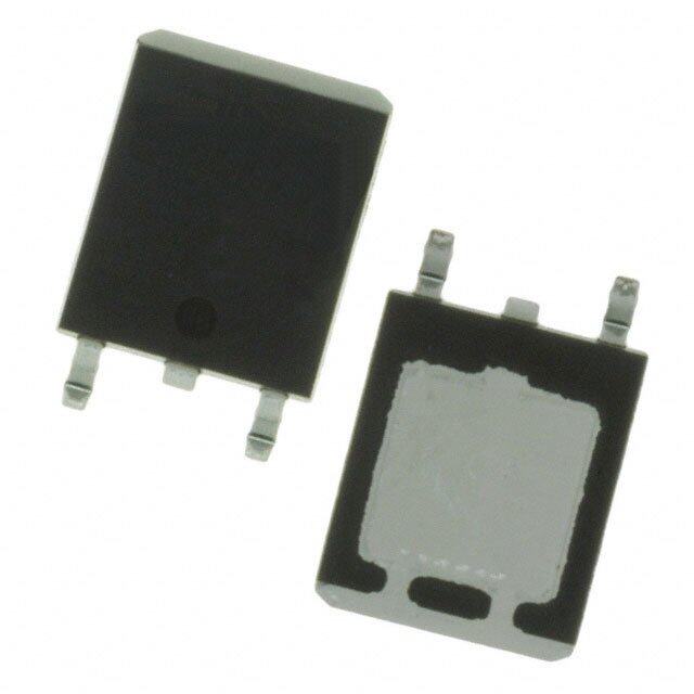
| 描述 | IC HIGH SIDE PWR SWITCH D2PAK-5 |
| 产品分类 | PMIC - MOSFET,电桥驱动器 - 内部开关 |
| 品牌 | Infineon Technologies |
| 数据手册 | http://www.infineon.com/dgdl/BTS441R_20030905.pdf?folderId=db3a304412b407950112b428ea4d3eb3&fileId=db3a304412b407950112b428eab93eb4http://www.infineon.com/dgdl/BTS441R_Green_DS_11.pdf?folderId=db3a304317a748360117eee5521349bb&fileId=db3a30431ed1d7b2011f473662665709 |
| 产品图片 |
|
| 产品型号 | BTS441RG |
| rohs | 无铅 / 符合限制有害物质指令(RoHS)规范要求 |
| 产品系列 | PROFET® |
| 产品目录页面 | |
| 供应商器件封装 | TO-263-5 |
| 其它名称 | BTS441RG-ND |
| 包装 | 带卷 (TR) |
| 安装类型 | 表面贴装 |
| 导通电阻 | 15 毫欧 |
| 封装/外壳 | TO-263-5,D²Pak(4 引线+接片),TO-263BB |
| 工作温度 | -40°C ~ 150°C |
| 标准包装 | 1,000 |
| 电压-电源 | 4.75 V ~ 43 V |
| 电流-峰值输出 | 65A |
| 电流-输出/通道 | 21A |
| 类型 | 高端 |
| 输入类型 | 非反相 |
| 输出数 | 1 |
.jpg)


- 商务部:美国ITC正式对集成电路等产品启动337调查
- 曝三星4nm工艺存在良率问题 高通将骁龙8 Gen1或转产台积电
- 太阳诱电将投资9.5亿元在常州建新厂生产MLCC 预计2023年完工
- 英特尔发布欧洲新工厂建设计划 深化IDM 2.0 战略
- 台积电先进制程称霸业界 有大客户加持明年业绩稳了
- 达到5530亿美元!SIA预计今年全球半导体销售额将创下新高
- 英特尔拟将自动驾驶子公司Mobileye上市 估值或超500亿美元
- 三星加码芯片和SET,合并消费电子和移动部门,撤换高东真等 CEO
- 三星电子宣布重大人事变动 还合并消费电子和移动部门
- 海关总署:前11个月进口集成电路产品价值2.52万亿元 增长14.8%


PDF Datasheet 数据手册内容提取
BTS441RG Smart Power High-Side-Switch One Channel 20 mΩ Data sheet Rev. 1.21, 2012-12-06 Automotive Power
Smart Power High-Side-Switch BTS441RG One Channel: 20 mΩ 1 Overview General Description • N channel vertical power FET with charge pump, ground referenced CMOS compatible input, monolithically integrated in Smart SIPMOS technology • Providing embedded protective functions • Green Product (RoHS compliant) • AEC Qualified Application PG-TO263-5 • µC compatible power switch 5 V, 12 V and 24 V DC applications • All types of resistive, inductive and capatitive loads • Most suitable for loads with high inrush currents, so as lamps • Replaces electromechanical relays, fuses and discrete circuits Basic Functions • Very low standby current • Optimized static electromagnetic compatibility (EMC) • µC and CMOS compatible • Fast demagnetization of inductive loads • Stable behavior at undervoltage Protection Functions BTS441RG • Short circuit protection VBB • Current limitation 3 • Overload protection • Thermal Shutdown • Overvoltage protection (including load dump) with Control external GND resistor 4 Circuit • Reverse battery protection with external GND-resistor ST • Loss of ground and loss of Vbb protection RIN TemSepnesraotrure OUT 5 • Electrostatic discharge (ESD) protection 2 GND IN Type Package Marking BTS441RG PG-TO263-5 BTS441R Data sheet 2 Rev. 1.21, 2012-12-06
BTS441RG Overview Diagnostic Function • Diagnostic feedback with open drain output • Open load detection in OFF-state • Feedback of thermal shutdown in ON-state Product Summary Maximum on-state resistance at T = 150 °C R 20 mΩ j DS(ON) Operating voltage V 4.75 V … 41 V SOP Nominal load current I 21 A L (nom) Current limitation I 65 A L(lim) Product Information Device Name Status Package Pins ECO status BTS441RG Active PG-TO263-5 5 Green BTS441RG Discontinued P-TO263-5 5 Gray BTS441RS Discontinued P-TO220-5 5 Gray BTS441RS Discontinued PG-TO220-5 5 Green Data sheet 3 Rev. 1.21, 2012-12-06
BTS441RG (cid:2)(cid:3)(cid:4)(cid:5)(cid:6)(cid:7)(cid:8)(cid:4)(cid:9)(cid:10)(cid:11)(cid:12)(cid:7)(cid:9)(cid:13)(cid:14)(cid:9)(cid:15)(cid:11) (cid:11)(cid:11) (cid:2) (cid:2) (cid:2) (cid:2) (cid:19)(cid:14)(cid:15)(cid:21)(cid:14)(cid:19)(cid:24)(cid:12)(cid:10)(cid:25)(cid:15)(cid:2) (cid:2) (cid:25)(cid:10)(cid:12)(cid:15)(cid:2) (cid:11)!(cid:21)(cid:21)(cid:15)(cid:22)(cid:12)(cid:2)(cid:24)(cid:13))(cid:13)(cid:12) (cid:27)++(cid:2) (cid:2) (cid:18)(cid:21)(cid:19)(cid:12)(cid:15)(cid:11)(cid:12)(cid:13)(cid:19)(cid:22) (cid:2) (cid:11)(cid:19)(cid:22)(cid:12)(cid:21)(cid:19)(cid:24)(cid:2) (cid:2) (cid:2) *(cid:2) (cid:2) (cid:13)(cid:22)(cid:12)(cid:15)(cid:21)(cid:22)(cid:10)(cid:24)(cid:2) (cid:2) (cid:11)(cid:17)(cid:10)(cid:21)(cid:25)(cid:15)(cid:2) (cid:2) (cid:11)(cid:24)(cid:10))(cid:18)(cid:2)(cid:23)(cid:19)(cid:21)(cid:2) (cid:14)(cid:19)(cid:24)(cid:12)(cid:10)(cid:25)(cid:15)(cid:2)(cid:16)!(cid:18)(cid:18)(cid:24)’(cid:2) (cid:24)(cid:19)(cid:25)(cid:13)(cid:11)(cid:2) (cid:18)!)(cid:18)(cid:2) (cid:2) (cid:13)(cid:22)(cid:30)!(cid:11)(cid:12)(cid:13)(cid:14)(cid:15)(cid:2)(cid:24)(cid:19)(cid:10)(cid:30) (cid:2) #$(cid:29)(cid:2) (cid:2) (cid:2) (cid:12)(cid:15))(cid:18)(cid:15)(cid:21)(cid:10)(cid:12)!(cid:21)(cid:15)(cid:2) (cid:2) (cid:8)(cid:5)(cid:2) (cid:2) (cid:16)(cid:15)(cid:22)(cid:16)(cid:19)(cid:21)(cid:2) (cid:2) ( (cid:6)(cid:2) (cid:2) ,#-(cid:6)(cid:2) (cid:2) #(cid:18)(cid:15)(cid:22)(cid:2)(cid:24)(cid:19)(cid:10)(cid:30)(cid:2) (cid:2) (cid:29)(cid:2) (cid:30)(cid:15)(cid:12)(cid:15)(cid:11)(cid:12)(cid:13)(cid:19)(cid:22)(cid:2) (cid:2) (cid:2) (cid:4)(cid:5)(cid:6)(cid:2) (cid:2) PROFET (cid:2) (cid:2) (cid:2) (cid:2) (cid:2) (cid:2) (cid:2) (cid:2) (cid:16)(cid:7)(cid:4)(cid:11)(cid:5)(cid:8)(cid:4)(cid:19)(cid:7)(cid:13)(cid:3)(cid:14)(cid:9)(cid:6)(cid:7)(cid:8)(cid:4)(cid:11)(cid:11) (cid:16)(cid:7)(cid:4)(cid:11)(cid:17)(cid:18)(cid:19)(cid:7)(cid:4)(cid:7)(cid:6)(cid:7)(cid:8)(cid:4)(cid:20)(cid:11)(cid:9)(cid:4)(cid:12)(cid:11)(cid:2)(cid:3)(cid:4)(cid:5)(cid:6)(cid:7)(cid:8)(cid:4)(cid:20)(cid:11) (cid:11) (cid:11) (cid:11) (cid:11)(cid:2)(cid:2)(cid:2)(cid:2)%(cid:12)(cid:19)(cid:18)(cid:2)(cid:14)(cid:13)(cid:15)(cid:20)&(cid:2) (cid:16)(cid:7)(cid:4)(cid:11) (cid:21)(cid:22)(cid:15)(cid:23)(cid:8)(cid:10)(cid:2) (cid:2)(cid:3)(cid:4)(cid:5)(cid:6)(cid:7)(cid:8)(cid:4)(cid:2) (cid:2) (cid:3)(cid:2) (cid:4)(cid:5)(cid:6)(cid:2) (cid:24)(cid:8)(cid:13)(cid:7)(cid:5)(cid:11)(cid:13)(cid:14)(cid:8)(cid:3)(cid:4)(cid:12)(cid:2) (cid:31)(cid:9)(cid:23)(cid:11) (cid:11)!"" (cid:25)(cid:4)(cid:26)(cid:3)(cid:6)(cid:9)(cid:2)(cid:10)(cid:11)(cid:12)(cid:13)(cid:14)(cid:10)(cid:12)(cid:15)(cid:16)(cid:2)(cid:12)(cid:17)(cid:15)(cid:2)(cid:18)(cid:19)(cid:20)(cid:15)(cid:21)(cid:2)(cid:16)(cid:20)(cid:13)(cid:12)(cid:11)(cid:17)(cid:2)(cid:13)(cid:22)(cid:2) (cid:7)(cid:2) (cid:8)(cid:5)(cid:2) (cid:11)(cid:10)(cid:16)(cid:15)(cid:2)(cid:19)(cid:23)(cid:2)(cid:24)(cid:19)(cid:25)(cid:13)(cid:11)(cid:10)(cid:24)(cid:2)(cid:17)(cid:13)(cid:25)(cid:17)(cid:2)(cid:16)(cid:13)(cid:25)(cid:22)(cid:10)(cid:24)(cid:2) (cid:16)(cid:8)(cid:20)(cid:7)(cid:6)(cid:7)(cid:27)(cid:18)(cid:11)(cid:26)(cid:8)(cid:28)(cid:18)(cid:14)(cid:11)(cid:20)(cid:3)(cid:26)(cid:26)(cid:10)(cid:22)(cid:11)(cid:27)(cid:8)(cid:10)(cid:6)(cid:9)(cid:13)(cid:18)(cid:11) (cid:26)(cid:2) (cid:27)(cid:28)(cid:28)(cid:2) (cid:29)(cid:17)(cid:15)(cid:2)(cid:12)(cid:10)(cid:28)(cid:2)(cid:13)(cid:16)(cid:2)(cid:16)(cid:17)(cid:19)(cid:21)(cid:12)(cid:15)(cid:30)(cid:2)(cid:12)(cid:19)(cid:2)(cid:18)(cid:13)(cid:22)(cid:2)(cid:26)(cid:2) (cid:31)(cid:2) (cid:29)(cid:2) (cid:17)(cid:7)(cid:9)(cid:13)(cid:4)(cid:8)(cid:20)(cid:6)(cid:7)(cid:5)(cid:11)(cid:19)(cid:18)(cid:18)(cid:12)(cid:23)(cid:9)(cid:5)(cid:29)(cid:9)(cid:2)(cid:24)(cid:19)(cid:20)(cid:2)(cid:19)(cid:22)(cid:2)(cid:23)(cid:10)(cid:13)(cid:24)!(cid:21)(cid:15)(cid:11) #(cid:11)(cid:11)(cid:11)(cid:11)(cid:11)(cid:11)$(cid:11)(cid:11)(cid:11)(cid:11)(cid:11)%&’(cid:11)(cid:11)(cid:11)(cid:11)(cid:11)(cid:11)((cid:11)(cid:11)(cid:11)(cid:11)(cid:11)(cid:11)) *+(cid:17)(cid:11)(cid:11)(cid:25)+(cid:11)(cid:11)(cid:11)(cid:11)(cid:11)(cid:11)(cid:11)(cid:11)(cid:11)(cid:11)(cid:11)(cid:11)(cid:11)(cid:21)(cid:31)(cid:11)(cid:11)(cid:30),(cid:31) (cid:2) "(cid:2) #$(cid:29)(cid:2) (cid:30)(cid:3)(cid:6)(cid:26)(cid:3)(cid:6)(cid:11)(cid:12)(cid:19)(cid:2)(cid:12)(cid:17)(cid:15)(cid:2)(cid:24)(cid:19)(cid:10)(cid:30)(cid:11) (cid:2) (cid:16)(cid:8)(cid:20)(cid:7)(cid:6)(cid:7)(cid:27)(cid:18)(cid:11)(cid:26)(cid:8)(cid:28)(cid:18)(cid:14)(cid:11)(cid:20)(cid:3)(cid:26)(cid:26)(cid:10)(cid:22)(cid:11)(cid:27)(cid:8)(cid:10)(cid:6)(cid:9)(cid:13)(cid:18)(cid:11) (cid:29)(cid:10)(cid:28)(cid:2) (cid:27)(cid:28)(cid:28)(cid:2) (cid:29)(cid:17)(cid:15)(cid:2)(cid:12)(cid:10)(cid:28)(cid:2)(cid:13)(cid:16)(cid:2)(cid:16)(cid:17)(cid:19)(cid:21)(cid:12)(cid:15)(cid:30)(cid:2)(cid:12)(cid:19)(cid:2)(cid:18)(cid:13)(cid:22)(cid:2)(cid:26)(cid:2) (cid:2) Data sheet 4 Rev. 1.21, 2012-12-06
BTS441RG Maximum Ratings at Tj = 25 °C unless otherwise specified Parameter Symbol Values Unit Supply voltage (overvoltage protection see page 4) V 43 V bb Supply voltage for full short circuit protection V 34 V bb T =-40 ...+150°C j Start Load dump protection1)V = V + V , V = 13.5 V V 3) 60 V LoadDump A s A Load dump R2)= 2 Ω, R = 0,5 Ω, t = 200 ms, IN= low or high I L d Load current (Short-circuit current, see page 5) I self-limited A L Operating temperature range T -40 ...+150 °C j T -55 ...+150 Storage temperature range stg Power dissipation (DC) ; TC≤25°C P 125 W tot Maximal switchable inductance, single pulse V =12V, T =150°C, T =150°C const. bb j,start C (see diagram, p.7) I =21A, RL= 0 Ω: E4) =0.7J: Z 2.1 mH L(ISO) AS L Electrostatic discharge capability (ESD) IN: V 1.0 kV ESD (Human Body Model) ST: 4.0 Out to all other pins shorted: 8.0 acc. MIL-STD883D, method 3015.7 and ESD assn. std. S5.1-1993; R=1.5kΩ; C=100pF Input voltage (DC) V -10 ... +16 V IN Current through input pin (DC) I ±2.0 mA IN Current through status pin (DC) I ±5.0 ST see internal circuit diagrams page 7 Thermal resistance chip - case: R ≤ 1 K/W thJC R ≤ 75 junction - ambient (free air): thJA SMD version, device on pcb5): ≤ 33 1) Supply voltages higher than V require an external current limit for the GND pin, e.g. with a 150 Ω bb(AZ) resistor in the GND connection. A resistor for the protection of the input is integrated. 2) R = internal resistance of the load dump test pulse generator I 3) V is setup without the DUT connected to the generator per ISO 7637-1 and DIN 40839 Load dump 4) EASis the maximum inductive switch off energy 5) Device on 50mm*50mm*1.5mm epoxy PCB FR4 with 6cm2 (one layer, 70μm thick) copper area for Vbb connection. PCB is vertical without blown air. Data sheet 5 Rev. 1.21, 2012-12-06
BTS441RG Electrical Characteristics Parameter and Conditions Symbol Values Unit atTj =-40...+150°C, Vbb = 12 V unless otherwise specified min typ max Load Switching Capabilities and Characteristics On-state resistance (Vbb (pin3) to OUT (pin5)); IL = 2 A Vbb≥7V: Tj=25 °C: RON -- 15 20 mΩ T=150 °C: 28 37 j see diagram page 9 Nominal load current (pin 3 to 5) IL(ISO) 17 21 -- A ‘ISO 10483-1, 6.7:V =0.5V,T=85°C ON C Output current (pin 5) while GND disconnected or IL(GNDhigh) -- -- 2 mA GND pulled up6), Vbb=30 V, VIN= 0, see diagram page 7 Turn-on time IN to 90% V : t 40 90 200 μs OUT on Turn-off time IN to 10% V : t 40 110 250 OUT off RL = 12 Ω, Slew rate on dV /dt 0.1 -- 1 V/μs on 10 to 30% VOUT,RL= 12 Ω, Slew rate off -dV/dt 0.1 -- 1 V/μs off 70 to 40% VOUT, RL= 12 Ω, Operating Parameters Operating voltage Tj =-40°C Vbb(on) 4.75 -- 41 V Tj =+25°C 4.75 -- 43 Tj =+105°C6) 4.75 -- 43 Tj =+150°C 5.0 -- 43 Overvoltage protection7) T =-40°C: V 41 -- -- V j bb(AZ) Ibb=40 mA Tj =+25...+150°C: 43 47 52 Standby current (pin 3) 8) Tj=-40...+25°C: Ibb(off) -- 5 10 μA T=+105°C6): -- -- 10 j VIN=0 see diagram page 9 Tj=+150°C: -- -- 25 Off-State output current (included in Ibb(off)) IL(off) -- 1.5 10 μA VIN=0 Operating current (Pin 1)9), V =5 V, I -- 2 4 mA IN GND 6) not subject to production test, specified by design 7) see also VON(CL) in table of protection functions and circuit diagram page 7 8) Measured with load, typ. 40 µA when no load in off 9) Add IST, if IST > 0, add IIN, if VIN>5.5 V Data sheet 6 Rev. 1.21, 2012-12-06
BTS441RG Parameter and Conditions Symbol Values Unit atTj =-40...+150°C, Vbb = 12 V unless otherwise specified min typ max Protection Functions10) Current limit (pin 3 to 5) T =-40°C: I -- -- 85 A j L(lim) (see timing diagrams, page 9) Tj =25°C: -- 65 -- T =+150°C: 40 -- -- j Repetitive short circuit current limit I -- 55 -- A L(SCr) Tj = Tjt (see timing diagrams, page 10) Thermal shutdown time11)12) T =25°C: T -- 14 -- ms j,start off(SC) (see timing diagram on page 10) Output clamp (inductive load switch off) ;Tj =-40°C: 41 -- -- V at VOUT = Vbb - VON(CL), IL= 40 mA Tj=25..150°C: VON(CL) 43 47 52 Thermal overload trip temperature T 150 -- -- °C jt Thermal hysteresis ΔT -- 10 -- K jt Reverse battery (pin 3 to 1) 13) -V -- -- 32 V bb Reverse battery voltage drop (V > V ) -V I = -2A OUT bTb =+150°C: ON(rev) -- 540 -- mV L j 10) Integrated protection functions are designed to prevent IC destruction under fault conditions described in the data sheet. Fault conditions are considered as "outside" normal operating range. Protection functions are not designed for continuous repetitive operation. 11) not subject to production test, specified by design 12) Device on 50mm*50mm*1.5mm epoxy PCB FR4 with 6cm2 (one layer, 70μm thick) copper area for Vbb connection. PCB is vertical without blown air. 13) Requires 150 Ω resistor in GND connection. The reverse load current through the intrinsic drain-source diode has to be limited by the connected load. Note that the power dissipation is higher compared to normal operating conditions due to the voltage drop across the intrinsic drain-source diode. The temperature protection is not active during reverse current operation! Input and Status currents have to be limited (see max. ratings page 1 and circuit page 7). Data sheet 7 Rev. 1.21, 2012-12-06
BTS441RG Parameter and Conditions Symbol Values Unit atTj =-40...+150°C, Vbb = 12 V unless otherwise specified min typ max Diagnostic Characteristics Open load detection voltage14) V 2 3 4 V OUT(OL)1 Input and Status Feedback15) Input resistance see circuit page 7 RI 2.5 3.8 6.5 kΩ Input turn-on threshold voltage V 1.2 -- 2.2 V IN(T+) Input turn-off threshold voltage V 0.8 -- -- V IN(T-) Input threshold hysteresis Δ V -- 0.3 -- V IN(T) Off state input current (pin 2) V = 0.4 V: I 1 -- 15 μA IN IN(off) On state input current (pin 2) V = 5 V: I 4.5 12 24 μA IN IN(on) Delay time for status with open load after switch t -- -- 500 μs ST delay off (see timing diagrams, page 11), Status output (open drain) Zener limit voltage I = +1.6 mA: V 5.4 6.1 -- V ST ST(high) ST low voltage I = +1.6 mA:: V -- -- 0.4 ST ST(low) Truth Table IN OUT ST Normal operation L L H H H H Open load L Z L16) H H H Short circuit to Vbb L H L H H H Overtemperature L L H H L L L = "Low" Level Z = high impedance, potential depends on external circuit H = "High" Level Status signal valid after the time delay shown in the timing diagrams 14) External pull up resistor required for open load detection in off state 15) If a ground resistor R is used, add the voltage drop across this resistor. GND 16) L, if potential at the Output exceeds the OpenLoad detection voltage Data sheet 8 Rev. 1.21, 2012-12-06
BTS441RG Overvolt. and reverse batt. protection Terms *(cid:2)"(cid:27) *(cid:2)(cid:27)(cid:28)(cid:28) (cid:8)(cid:28)(cid:28) . (cid:27)(cid:28)(cid:28) (cid:8)(cid:8)(cid:5) (cid:27)(cid:28),(cid:28)(cid:15)(cid:10)(cid:30)(cid:23)(cid:21)(cid:10))(cid:15)(cid:9)(cid:2)(cid:26) (cid:29) (cid:8)(cid:5) .(cid:8) (cid:27)0(cid:7) (cid:8)(cid:5) (cid:7) (cid:8), (cid:27)#(cid:5) (cid:24)(cid:8)(cid:13)(cid:7)(cid:5) (cid:27)(cid:8)(cid:5) (cid:8) (cid:29) (cid:16)-(cid:30)(cid:2).(cid:31) #$(cid:29) " . (cid:29) (cid:29) #$(cid:29) (cid:29) (cid:27) (cid:29) (cid:31) (cid:4)(cid:5)(cid:6) (cid:27)0(cid:3) 1.#2((cid:29) (cid:3) .(cid:4)(cid:5)(cid:6) (cid:8)(cid:4)(cid:5)(cid:6) (cid:27)#$(cid:29) .(cid:4)(cid:5)(cid:6) (cid:4)(cid:5)(cid:6) .,(cid:19)(cid:10)(cid:30) (cid:13)(cid:25)(cid:22)(cid:10)(cid:24)(cid:2)(cid:4)(cid:5)(cid:6) ,(cid:19)(cid:10)(cid:30)(cid:2)(cid:4)(cid:5)(cid:6) VZ1 = 6.1 V typ., VZ2 = 47 V typ., RGND = 150 Ω, RST= 15 kΩ,RI= 3.5 kΩ typ. Input circuit (ESD protection) In case of reverse battery the load current has to be limited by the load. Temperature protection is not . active (cid:8) (cid:8)(cid:5) Open-load detection ( (cid:6)/0(cid:6) (cid:8) (cid:8)(cid:8) OFF-state diagnostic condition: (cid:4)(cid:5)(cid:6) Open Load, if VOUT > 3 V typ.; IN low The use of ESD zener diodes as voltage clamp at DC (cid:27)(cid:28)(cid:28) conditions is not recommended. Status output . (3(cid:29) #22 *"(cid:27) (cid:27) #$(cid:29) . (cid:29)%#(cid:5)& (cid:29) ,(cid:19)(cid:25)(cid:13)(cid:11) (cid:30)(cid:26)(cid:18)(cid:4)(cid:11)(cid:10)(cid:8)(cid:9)(cid:12) !(cid:22)(cid:13)(cid:12) (cid:12)(cid:18)(cid:6)(cid:18)(cid:5)(cid:6)(cid:7)(cid:8)(cid:4) ( (cid:6)/ 0(cid:6) (cid:4)(cid:5)(cid:6) (cid:13)(cid:25)(cid:22)(cid:10)(cid:24)(cid:2)(cid:4)(cid:5)(cid:6) ESD-Zener diode: 6.1V typ., max 5.0 mA; RST(ON) < 375 Ω at 1.6 mA, ESD zener diodes are not to be used as voltage GND disconnect clamp at DC conditions. Operation in this mode may resultin (cid:11) a drift ofthe zener voltage (increase of up to 1 V). Inductive and overvoltage output clamp (cid:27) (cid:8)(cid:5) (cid:28)(cid:28) *(cid:2)(cid:27)(cid:28)(cid:28) (cid:27) (cid:16)-(cid:30)(cid:2).(cid:31) #$(cid:29) 0 (cid:29) (cid:27) (cid:4)(cid:5)(cid:6) #(cid:5) (cid:27)(cid:28)(cid:28) (cid:27)(cid:8)(cid:5) (cid:27) (cid:29) (cid:27)(cid:4)(cid:5)(cid:6) #$(cid:29) 1.#2((cid:29) (cid:4)(cid:5)(cid:6) Any kind of load. In case of Input=high is VOUT ≈ VIN - VIN(T+) . VON clamped to 47 V typ. Data sheet 9 Rev. 1.21, 2012-12-06
BTS441RG Inductive load switch-off energy dissipation GND disconnect with GND pull up ((cid:28)(cid:28) (cid:11) (- ( (cid:8)(cid:5) (cid:27)(cid:28)(cid:28) (cid:8)(cid:5) (cid:27)(cid:28)(cid:28) ,(cid:19)(cid:10)(cid:30) (cid:16)-(cid:30)(cid:2).(cid:31) #$(cid:29) (cid:16)-(cid:30)(cid:2).(cid:31) #$(cid:29) (cid:29) , (cid:4)(cid:5)(cid:6) (cid:29) (cid:2) (, (cid:4)(cid:5)(cid:6) 0 , (cid:27)(cid:28)(cid:28) (cid:27)(cid:8)(cid:5)(cid:27) (cid:29) (cid:27)(cid:4)(cid:5)(cid:6) . (. , Any kind of load. If VGND > VIN - VIN(T+) device stays off Energy stored in load inductance: Due to VGND >0, no VST = low signal available. Vbb disconnect with charged inductive EL = 1/2·L·I2L load While demagnetizing load inductance, the energy dissipated in PROFET is EAS= Ebb + EL - ER= VON(CL)·iL(t) dt, (cid:17)(cid:13)(cid:25)(cid:17) (cid:8)(cid:5) (cid:27)(cid:28)(cid:28) with an approximate solution for RL> 0Ω: (cid:16)-(cid:30)(cid:2).(cid:31) #$(cid:29) EAS=2IL·R·LL(Vbb+|VOUT(CL)|) (cid:2)(cid:3)(cid:4)(1+ |VOILU·TR(CLL)| ) (cid:29) (cid:4)(cid:5)(cid:6) Maximum allowable load inductance for a single switch off (cid:27)(cid:28)(cid:28) (cid:2)(cid:3)(cid:4)(cid:3)(cid:5)(cid:3)(cid:6)(cid:7)(cid:2)(cid:3)(cid:8)(cid:9)(cid:3)Tj,start =150°C, Vbb=12V, RL=0Ω L [mH] For inductive load currents up to the limits defined by ZL (cid:3)444 (max. ratings and diagram on page 8) each switch is protected against loss of Vbb. Consider at your PCB layout that in the case of Vbb dis- connection with energized inductive load all the load current flows through the GND connection. (cid:3)44 (cid:3)4 (cid:3) 45(cid:3) 4 " (cid:3)4 (cid:3)" (cid:7)4 (cid:7)" (cid:26)4 (cid:26)" IL [A] Data sheet 10 Rev. 1.21, 2012-12-06
BTS441RG Typ. on-state resistance (cid:10)(cid:11)(cid:12)(cid:3)(cid:4)(cid:3)(cid:5)(cid:3)(cid:6)(cid:13)(cid:14)(cid:14)(cid:15)(cid:16)(cid:17)(cid:3)(cid:8); IL=2A, IN= high R [mΩ] ON (cid:31)4 (cid:29)8(cid:2)9(cid:2)(cid:3)"4:; (cid:26)" (cid:26)4 (cid:7)" (cid:7)4 (cid:7)":; (cid:3)" /(cid:31)4:; (cid:3)4 " (cid:26)(cid:2)(cid:2)(cid:2)(cid:2)(cid:2)(cid:2)(cid:2)"(cid:2)(cid:2)(cid:2)(cid:2)(cid:2)(cid:2)(cid:2)6(cid:2)(cid:2)(cid:2)(cid:2)(cid:2)(cid:2)(cid:2)7 (cid:26)4 (cid:31)4 Vbb [V] Typ. standby current (cid:7)(cid:14)(cid:14)(cid:6)(cid:18)(cid:5)(cid:5)(cid:8)(cid:3)(cid:4)(cid:3)(cid:5)(cid:3)(cid:6)(cid:16)(cid:17)(cid:3)(cid:8);Vbb= 9...34 V, IN1,2= low I [μA] bb(off) (cid:7)4 (cid:3)" (cid:3)4 " 4 /"4 4 "4 (cid:3)44 (cid:3)"4 (cid:7)44 Tj [°C] Data sheet 11 Rev. 1.21, 2012-12-06
BTS441RG Timing diagrams Figure 1a: Vbb turn on: Figure 2b: Switching a lamp, (cid:8)(cid:5) (cid:8)(cid:5) (cid:27) (cid:28)(cid:28) (cid:29) (cid:27) #$(cid:29) (cid:27) #$(cid:29) (cid:8) (cid:29)(cid:2)(cid:19)(cid:18)(cid:15)(cid:22)(cid:2)(cid:30)(cid:21)(cid:10)(cid:13)(cid:22) , (cid:12) (cid:12) (cid:11) (cid:2) proper turn on under all conditions Figure 2a: Switching a resistive load, Figure 3a: Short circuit turn-on/off time and slew rate definition: shut down by overtemperature, reset by cooling (cid:8)(cid:5) (cid:8)(cid:5) (cid:19)(cid:12)(cid:17)(cid:15)(cid:21)(cid:2)(cid:11)(cid:17)(cid:10)(cid:22)(cid:22)(cid:15)(cid:24)>(cid:2)(cid:22)(cid:19)(cid:21))(cid:10)(cid:24)(cid:2)(cid:19)(cid:18)(cid:15)(cid:21)(cid:10)(cid:12)(cid:13)(cid:19)(cid:22) (cid:27) #$(cid:29) 74< (cid:8) (cid:12) (cid:30)(cid:27)=(cid:30)(cid:12)(cid:19)(cid:23)(cid:23) , on (cid:8) (cid:30)(cid:27)=(cid:30)(cid:12)(cid:19)(cid:22) (cid:12) ,%(cid:24)(cid:13))& off (cid:3)4< (cid:8) ,% ;(cid:21)& (cid:8) , (cid:12) (cid:19)(cid:23)(cid:23)% ;& (cid:29) (cid:12) (cid:12) Heating up may require several milliseconds, depending on external conditions Data sheet 12 Rev. 1.21, 2012-12-06
BTS441RG Figure 4a: Overtemperature: Reset if Tj <Tjt (cid:8)(cid:5) (cid:29) (cid:27) #$(cid:29) (cid:29) ? (cid:12) Figure 5a: Open load: detection in OFF-state, turn on/off to open load (cid:8)(cid:5)(cid:3) (cid:2) (cid:27) (cid:11)(cid:12)(cid:12) #$(cid:29)(cid:3) (cid:8) ,(cid:3) (cid:2) (cid:3)(cid:4)(cid:5)(cid:6)(cid:7)(cid:8)(cid:9)(cid:10) (cid:29) t . = 500µs ST delay Open load detection requires an external pull up resistor between OUT and VBB Data sheet 13 Rev. 1.21, 2012-12-06
BTS441RG Package Outlines 4.4 10±0.2 1.27±0.1 0...0.3 A B 8.51) 3 0.05 0. ± 1 2.4 (15) 9.25±0.2 1)7.55 1.3±0.3 5 0.30.1 ±0. 7± 7 2. 4. 0...0.15 5 x 0.8±0.1 0.5±0.1 4 x 1.7 8˚ MAX. 0.25 M A B 0.1 B 1) Typical Metal surface min. X = 7.25, Y = 6.9 All metal surfaces tin plated, except area of cut. GPT09062 Figure 6: PG-TO263-5-2 Green Product (RoHS compliant) To meet the world-wide customer requirements for environmentally friendly products and to be compliant with government regulations the device is available as a green product. Green products are RoHS-Compliant (i.e Pb-free finish on leads and suitable for Pb-free soldering according to IPC/JEDEC J-STD-020). For further information on alternative packages, please visit our website: http://www.infineon.com/packages. Dimensions in mm Data sheet 14 Rev. 1.21, 2012-12-06
BTS441RG Revision History Revision Date Changes 1.21 2012-12-06 Device marking correction on page overview. 1.20 2012-06-27 Remove PG-TO-220-5-12 package on page overview and in package outlines. Added coverpage. 1.1 2009-01-30 RoHS-compliant PG-TO220 and PG-TO263 packages version of the BTS441R All pages: Infineon logo updated Page 1: Added “AEC Qualified” and “RoHS” logo, added “Green Product (RoHS compliant)” and “AEC Qualified” statement to feature list, package names changed to RoHS compliant versions, updated package drawing. Page 12-13: Package names changed to RoHS compliant versions ( PG-TO220-12 and PG- TO263-5-2), added “Green Product” description added Revision History added Legal Disclaimer Data sheet 15 Rev. 1.21, 2012-12-06
Edition 2012-12-06 Published by Infineon Technologies AG 81726 Munich, Germany © 2012 Infineon Technologies AG All Rights Reserved. Legal Disclaimer The information given in this document shall in no event be regarded as a guarantee of conditions or characteristics. With respect to any examples or hints given herein, any typical values stated herein and/or any information regarding the application of the device, Infineon Technologies hereby disclaims any and all warranties and liabilities of any kind, including without limitation, warranties of non-infringement of intellectual property rights of any third party. Information For further information on technology, delivery terms and conditions and prices, please contact the nearest Infineon Technologies Office (www.infineon.com). Warnings Due to technical requirements, components may contain dangerous substances. For information on the types in question, please contact the nearest Infineon Technologies Office. Infineon Technologies components may be used in life-support devices or systems only with the express written approval of Infineon Technologies, if a failure of such components can reasonably be expected to cause the failure of that life-support device or system or to affect the safety or effectiveness of that device or system. Life support devices or systems are intended to be implanted in the human body or to support and/or maintain and sustain and/or protect human life. If they fail, it is reasonable to assume that the health of the user or other persons may be endangered.
Mouser Electronics Authorized Distributor Click to View Pricing, Inventory, Delivery & Lifecycle Information: I nfineon: BTS441RG