ICGOO在线商城 > 分立半导体产品 > 晶闸管 - TRIAC > BTB10-600BWRG

 Datasheet下载
- 型号: BTB10-600BWRG
- 制造商: STMicroelectronics
- 库位|库存: xxxx|xxxx
- 要求:
| 数量阶梯 | 香港交货 | 国内含税 |
| +xxxx | $xxxx | ¥xxxx |
查看当月历史价格
查看今年历史价格
BTB10-600BWRG产品简介:
ICGOO电子元器件商城为您提供BTB10-600BWRG由STMicroelectronics设计生产,在icgoo商城现货销售,并且可以通过原厂、代理商等渠道进行代购。 BTB10-600BWRG价格参考。STMicroelectronicsBTB10-600BWRG封装/规格:晶闸管 - TRIAC, TRIAC Alternistor - Snubberless 600V 10A Through Hole TO-220AB。您可以下载BTB10-600BWRG参考资料、Datasheet数据手册功能说明书,资料中有BTB10-600BWRG 详细功能的应用电路图电压和使用方法及教程。
| 参数 | 数值 |
| 产品目录 | |
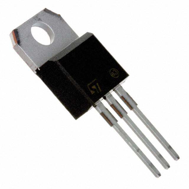
| 描述 | TRIAC ALTERNISTOR 600V TO220AB双向可控硅 10 Amp 600 Volt |
| 产品分类 | 双向可控硅分离式半导体 |
| GateTriggerCurrent-Igt | 50 mA |
| GateTriggerVoltage-Vgt | 1.3 V |
| 品牌 | STMicroelectronics |
| 产品手册 | |
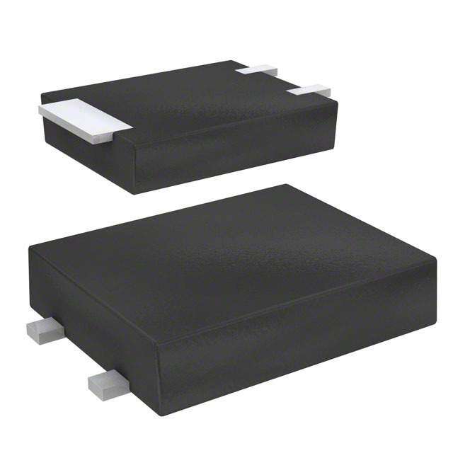
| 产品图片 |
|
| rohs | 符合RoHS无铅 / 符合限制有害物质指令(RoHS)规范要求 |
| 产品系列 | 晶体闸流管,双向可控硅,STMicroelectronics BTB10-600BWRGSnubberless™ |
| 数据手册 | |
| 产品型号 | BTB10-600BWRG |
| 三端双向可控硅类型 | 可控硅 - 无缓冲器 |
| 不重复通态电流 | 105 A |
| 产品培训模块 | http://www.digikey.cn/PTM/IndividualPTM.page?site=cn&lang=zhs&ptm=26297http://www.digikey.cn/PTM/IndividualPTM.page?site=cn&lang=zhs&ptm=26298 |
| 产品目录页面 | |
| 产品种类 | 双向可控硅 |
| 供应商器件封装 | TO-220AB |
| 保持电流Ih最大值 | 50 mA |
| 关闭状态漏泄电流(在VDRMIDRM下) | 5 uA |
| 其它名称 | 497-6676-5 |
| 其它有关文件 | http://www.st.com/web/catalog/sense_power/FM144/CL1221/SC124/PF76123?referrer=70071840 |
| 包装 | 管件 |
| 商标 | STMicroelectronics |
| 安装类型 | 通孔 |
| 安装风格 | Through Hole |
| 封装 | Tube |
| 封装/外壳 | TO-220-3 |
| 封装/箱体 | TO-220-3 |
| 工厂包装数量 | 50 |
| 开启状态电压 | 1.55 V |
| 最大工作温度 | + 125 C |
| 最大转折电流IBO | 105 A |
| 最小工作温度 | - 40 C |
| 栅极触发电压-Vgt | 1.3 V |
| 栅极触发电流-Igt | 50 mA |
| 标准包装 | 50 |
| 电压-断态 | 600V |
| 电压-栅极触发(Vgt)(最大值) | 1.3V |
| 电流-不重复浪涌50、60Hz(Itsm) | 100A,105A |
| 电流-保持(Ih)(最大值) | 50mA |
| 电流-栅极触发(Igt)(最大值) | 50mA |
| 电流-通态(It(RMS))(最大值) | 10A |
| 系列 | BTB10 |
| 配置 | 单一 |
| 额定重复关闭状态电压VDRM | 600 V |


- 商务部:美国ITC正式对集成电路等产品启动337调查
- 曝三星4nm工艺存在良率问题 高通将骁龙8 Gen1或转产台积电
- 太阳诱电将投资9.5亿元在常州建新厂生产MLCC 预计2023年完工
- 英特尔发布欧洲新工厂建设计划 深化IDM 2.0 战略
- 台积电先进制程称霸业界 有大客户加持明年业绩稳了
- 达到5530亿美元!SIA预计今年全球半导体销售额将创下新高
- 英特尔拟将自动驾驶子公司Mobileye上市 估值或超500亿美元
- 三星加码芯片和SET,合并消费电子和移动部门,撤换高东真等 CEO
- 三星电子宣布重大人事变动 还合并消费电子和移动部门
- 海关总署:前11个月进口集成电路产品价值2.52万亿元 增长14.8%


PDF Datasheet 数据手册内容提取
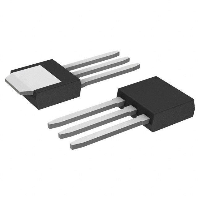
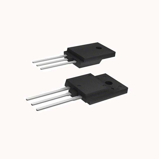
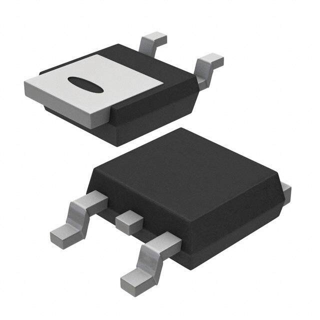
BTA10, BTB10 T1035, T1050 Datasheet 10 A Snubberless™, logic level and standard Triacs Features A2 • Medium current Triac • Low thermal resistance with clip bonding G • Low thermal resistance insulation ceramic for insulated BTA A1 • High commutation (4Q) or very high commutation (3Q, Snubberless™) A2 capability • BTA series UL1557 certified (file ref: 81734) • Packages are RoHS (2002/95/EC) compliant G G A2 A2 A1 A1 TO-220AB TO-220AB Ins. Description A2 Available either in through-hole or surface mount packages, the BTA10, BTB10 and T10xx Triac series are suitable for general purpose mains power AC switching. They A2 G can be used as ON/OFF function in applications such as static relays, heating A1 regulation or induction motor starting circuit. They are also recommended for phase D²PAK control operations in light dimmers and appliance motors speed controllers. The Snubberless™ versions (W suffix and T10xx) are especially recommended for use on inductive loads, because of their high commutation performance. By using an internal ceramic pad, the Snubberless™ series provide an insulated tab (rated at 2500 V ) complying with UL standards (file reference: E81734). RMS Product status link BTA10, BTB10, T1035, T1050 Product summary IT(RMS) 10 A VDRM/VRRM 600 and 800 V IGT 25 to 50 mA DS3165 - Rev 9 - March 2019 www.st.com For further information contact your local STMicroelectronics sales office.
BTA10, BTB10, T1035, T1050 Characteristics 1 Characteristics Table 1. Absolute maximum ratings Symbol Parameters Value Unit TO-220AB Tc = 105 °C IT(RMS) RMS on-state current (full sine wave) 10 A TO-220AB Ins. Tc = 95 °C ITSM Non repetitive surge peak on-state current (full cycle, Tj F = 50 Hz tp = 20 ms 100 A initial = 25 °C) F = 60 Hz tp = 16.7 ms 105 I2t I2t value for fusing tp = 10 ms 55 A2s Critical rate of rise of on-state current dl/dt F = 120 Hz Tj = 125 °C 50 A/µs IG = 2 x IGT , tr ≤ 100 ns VDSM/VRSM Non repetitive surge peak off-state voltage tp = 10 ms Tj = 25 °C VDRM/VRRM + V 100 IGM Peak gate current tp = 20 µs Tj = 125 °C 4 A PG(AV) Average gate power dissipation Tj = 125 °C 1 W Tstg Storage junction temperature range -40 to +150 °C Tj Operating junction temperature range -40 to +125 °C Table 2. Static electrical characteristics Symbol Test conditions Tj Value Unit VT(1) ITM = 14 A, tp = 380 µs 25 °C Max. 1.55 V VTO threshold on-state voltage 125 °C Max. 0.85 V RD Dynamic resistance 125 °C Max. 40 mΩ 25 °C 5 µA IDRM/IRRM VDRM = VRRM Max. 125 °C 1 mA 1. For both polarities of A2 referenced to A1 Table 3. Electrical characteristics (T = 25 °C, unless otherwise specified) - Snubberless™ (3 quadrants) j T1050 BTA10-xCW Symbol Parameters Quadrant T1035 BTA10-xBW Unit BTB10-xCW BTB10-xBW IGT I - II - III Max. 35 50 mA VD = 12 V, RL = 33 Ω VGT I - II - III Max. 1.3 V VGD VD = VDRM, RL = 3,3 kΩ, Tj = 125 °C I - II - III Min. 0.2 V IH IT = 500 mA I - II - III Max. 35 50 mA I - III Max. 50 70 IL IG = 1.2 IGT mA II Max. 80 60 80 dV/dt(2) VD = 67 % VDRM gate open, Tj = 125 °C Min. 500 1000 V/µs DS3165 - Rev 9 page 2/12
BTA10, BTB10, T1035, T1050 Characteristics T1050 BTA10-xCW Symbol Parameters Quadrant T1035 BTA10-xBW Unit BTB10-xCW BTB10-xBW (dI/dt)c(2) Without snubber, Tj = 125 °C Min. 5.5 9 A/ms 1. Minimum IGT is guaranteed at 5 % of IGT max. 2. For both polarities of A2 referenced to A1 Table 4. Electrical characteristics (T = 25 °C, unless otherwise specified) - standard Triac (4 quadrants) j Value Symbol Parameters Quadrant Unit C B I - II - III Max. 25 50 IGT(1) mA VD = 12 V, RL = 33 Ω IV Max. 50 100 VGT All Max. 1.3 V VGD VD = VDRM, RL = 3,3 kΩ, Tj = 125 °C I - II - III Min. 0.2 V IH(2) IT = 500 mA I - II - III Max. 25 50 mA I - III Max. 40 50 IL IG = 1.2 IGT mA II Max. 80 100 dV/dt(2) VD = 67 % VDRM gate open, Tj = 125 °C Min. 200 400 V/µs (dV/dt)c(2) (dI/dt)c = 4.4 A/ms, Tj = 125 °C Min. 5 10 V/µs 1. Minimum IGT is guaranteed at 5 % of IGT max. 2. For both polarities of A2 referenced to A1 Table 5. Thermal resistance Symbol Parameters Value Unit TO-220AB / D²PAK 1.5 Rth(j-c) (typ.) Junction to case (AC) TO-220AB insulated 2.4 °C/W Junction to ambient (S(1) = 2 cm²) D²PAK 45 Rth(j-a) (max.) Junction to ambient TO-220AB / TO-220AB ins 60 1. Copper surface under tab. DS3165 - Rev 9 page 3/12
BTA10, BTB10, T1035, T1050 Characteristics (curves) 1.1 Characteristics (curves) Figure 2. Maximum power dissipation versus on-state Figure 3. RMS on-state current versus case temperature RMS current (full cycle) (full cycle) P(W) IT(RMS)(A) 13 12 12 11 11 10 BTB/T10 10 9 9 8 BTA 8 7 7 6 6 5 5 4 4 3 3 2 2 1 IT(RMS)(A) 1 Tc(°C) 0 0 0 1 2 3 4 5 6 7 8 9 10 0 25 50 75 100 125 Figure 4. Relative variation of thermal impedance versus pulse duration Figure 5. On-state characteristics (maximum values) ITM(A) K = [Zth/Rth] 100 1E+0 Zth(j-c) VtoT j= m 0a.8x5. V Tj = Tj max. Rd = 40 mΩ Zth(j-a) 10 1E-1 Tj = 25 °C VTM(V) tp(s) 1 1E-2 0.5 1.0 1.5 2.0 2.5 3.0 3.5 4.0 4.5 5.0 1E-3 1E-2 1E-1 1E+0 1E+1 1E+2 5E+2 Figure 6. Surge peak on-state current versus number of Figure 7. Non repetitive surge peak on-state current cycles versus sinusoidal pulse width (t < 10 ms) P ITSM(A) ITSM(A) 1000 110 Tjinitial=25°C 100 90 80 Non repetitive t=20ms ITSM 70 Tjinitial=25°C One cycle dI/dt limitation: 50A/µs 60 100 50 40 Repetitive TC=95°C 30 20 10 Number of cycles tp(ms) 0 10 1 10 100 1000 0.01 0.10 1.00 10.00 DS3165 - Rev 9 page 4/12
BTA10, BTB10, T1035, T1050 Characteristics (curves) Figure 8. Relative variation of gate trigger current, holding Figure 9. Relative variation of critical rate of decrease of current and latching current versus junction temperature main current versus (dV/dt)c (typical values) (typical values) IGT,IH,IL[Tj] / IGT,IH,IL[Tj = 25 °C] (dl/dt)c [(dV/dt)c / specified (dl/dt)c 2.5 2.0 1.8 2.0 C 1.6 IGT B 1.4 1.5 1.2 BW/CW/T10xx 1.0 IH and IL 1.0 0.8 0.5 0.6 0.0 Tj (°C) 0.4 (dV/dt)c (V/µs) -40 -20 0 20 40 60 80 100 120 140 0.1 1.0 10.0 100.0 Figure 10. Relative variation of critical rate of decrease of Figure 11. D²PAK thermal resistance junction to ambient main current versus junction temperature versus copper surface under tab (dl/dt)c [Tj] / (dl/dt)c [Tj = 125 °C] 80 Rth(j-a)(°C/W) 6 D²PAK 70 Epoxy printed board FR4, copper thickness = 35 µm 5 60 4 50 3 40 30 2 20 1 10 Tj(°C) SCu(cm²) 0 0 0 25 50 75 100 125 0 5 10 15 20 25 30 35 40 DS3165 - Rev 9 page 5/12
BTA10, BTB10, T1035, T1050 Package information 2 Package information In order to meet environmental requirements, ST offers these devices in different grades of ECOPACK® packages, depending on their level of environmental compliance. ECOPACK® specifications, grade definitions and product status are available at: www.st.com. ECOPACK® is an ST trademark. 2.1 D²PAK package information Figure 12. D²PAK package outline E A E1 c2 E2 2 L 1 D D H 1 2 3 2 3 D L b2 e b Max resin gate protrusion: 0.5 mm (1) G A1 A2 A3 R L Gauge Plane c V2 (1) Resin gate is accepted in each of position shown on the drawing, or their symmetrical. Table 6. D²PAK package mechanical data Dimensions Ref. Millimeters Inches(1) Min. Typ. Max. Min. Typ. Max. A 4.30 4.60 0.1693 0.1811 A1 2.49 2.69 0.0980 0.1059 A2 0.03 0.23 0.0012 0.0091 A3 0.25 0.0098 b 0.70 0.93 0.0276 0.0366 b2 1.25 1.7 0.0492 0.0669 DS3165 - Rev 9 page 6/12
BTA10, BTB10, T1035, T1050 D²PAK package information Dimensions Ref. Millimeters Inches(1) Min. Typ. Max. Min. Typ. Max. c 0.45 0.60 0.0177 0.0236 c2 1.21 1.36 0.0476 0.0535 D 8.95 9.35 0.3524 0.3681 D1 7.50 8.00 0.2953 0.3150 D2 1.30 1.70 0.0512 0.0669 e 2.54 0.1 E 10.00 10.28 0.3937 0.4047 E1 8.30 8.70 0.3268 0.3425 E2 6.85 7.25 0.2697 0.2854 G 4.88 5.28 0.1921 0.2079 H 15 15.85 0.5906 0.6240 L 1.78 2.28 0.0701 0.0898 L2 1.27 1.40 0.0500 0.0551 L3 1.40 1.75 0.0551 0.0689 R 0.40 0.0157 V2 0° 8° 0° 8° 1. Dimensions in inches are given for reference only Figure 13. D²PAK recommended footprint (dimensions are in mm) 16.90 10.30 5.08 1.30 3.70 8.90 DS3165 - Rev 9 page 7/12
BTA10, BTB10, T1035, T1050 TO-220AB non ins. and insulated package information 2.2 TO-220AB non ins. and insulated package information Figure 14. TO-220AB non ins. and insulated package outline B C b2 I Resin gate 0.5 mm max. protusion(1) L F A I4 l3 c2 a1 l2 a2 M c1 b1 Resin gate 0.5 mm max. protusion(1) e (1)Resin gate position accepted in one of the two positions or in the symmetrical opposites. Table 7. TO-220AB non ins. and insulated package mechanical data Dimensions Ref. Millimeters Inches1 Min. Typ. Max. Min. Typ. Max. A 15.20 15.90 0.5984 0.6260 a1 3.75 0.1476 a2 13.00 14.00 0.5118 0.5512 B 10.00 10.40 0.3937 0.4094 b1 0.61 0.88 0.0240 0.0346 b2 1.23 1.32 0.0484 0.0520 C 4.40 4.60 0.1732 0.1811 DS3165 - Rev 9 page 8/12
BTA10, BTB10, T1035, T1050 TO-220AB non ins. and insulated package information Dimensions Ref. Millimeters Inches1 Min. Typ. Max. Min. Typ. Max. c1 0.49 0.70 0.0193 0.0276 c2 2.40 2.72 0.0945 0.1071 e 2.40 2.70 0.0945 0.1063 F 6.20 6.60 0.2441 0.2598 I 3.73 3.88 0.1469 0.1528 L 2.65 2.95 0.1043 0.1161 I2 1.14 1.70 0.0449 0.0669 I3 1.14 1.70 0.0449 0.0669 I4 15.80 16.40 16.80 0.6220 0.6457 0.6614 M 2.6 0.1024 1. Inch dimensions are for reference only. DS3165 - Rev 9 page 9/12
BTA10, BTB10, T1035, T1050 Ordering information 3 Ordering information Figure 15. BTA10 and BTB10 series ordering information scheme BT A 10 - 600 BW RG Triac Insulation A = Insulated B = Non-insulated Current 10 = 10 A Voltage 600 = 600 V 800 = 800 V Sensitivityand type B = 50 mA standard BW = 50 mA Snubberless™ C = 25 mA standard CW = 35 mA Snubberless™ Packing mode RG = Tube Figure 16. T10xx series ordering information scheme T 10 50 - 8 G - TR Triac Current 10 = 10 A Sensitivity 50 = 50 mA 35 = 35 mA Voltage 800 V 600 V Package G = D²PAK Packing mode (blank) = Tube -TR = Tape and reel Table 8. Ordering information Order code Marking Package Weight Base qty. Delivery mode BTA10-600BRG BTA10-600B BTA10-600CRG BTA10-600C BTA10-600BWRG BTA10-600BW TO-220AB Ins. BTA10-600CWRG BTA10-600CW 2.3 g BTA10-800BWRG BTA10-800BW 50 Tube BTA10-800CWRG BTA10-800CW BTB10-600BWRG BTB10-600BW TO-220AB BTB10-800BWRG BTB10-800BW T1035-6G T1035-6G T1050-8G T1050-8G D²PAK 1.50 g T1035-6G-TR T1035-6G 1000 Tape and reel 13" T1050-8G-TR T1050-8G DS3165 - Rev 9 page 10/12
BTA10, BTB10, T1035, T1050 Revision history Table 9. Document revision history Date Revision Changes Sep-2002 5A Last update. TO-220AB delivery mode changed from bulk to tube. ECOPACK statement 13-Feb-2006 6 added. 06-Feb-2017 7 Added D²PAK package information. Updated Table 3. Electrical characteristics (Tj = 25 °C, unless otherwise specified) - Snubberless™ (3 quadrants), Section 3 Ordering information and 15-Mar-2018 8 Section 2.1 D²PAK package information. Added RPNs T1035 and T1050. 01-Mar-2019 9 Updated Links syntax. DS3165 - Rev 9 page 11/12
BTA10, BTB10, T1035, T1050 IMPORTANT NOTICE – PLEASE READ CAREFULLY STMicroelectronics NV and its subsidiaries (“ST”) reserve the right to make changes, corrections, enhancements, modifications, and improvements to ST products and/or to this document at any time without notice. Purchasers should obtain the latest relevant information on ST products before placing orders. ST products are sold pursuant to ST’s terms and conditions of sale in place at the time of order acknowledgement. Purchasers are solely responsible for the choice, selection, and use of ST products and ST assumes no liability for application assistance or the design of Purchasers’ products. No license, express or implied, to any intellectual property right is granted by ST herein. Resale of ST products with provisions different from the information set forth herein shall void any warranty granted by ST for such product. ST and the ST logo are trademarks of ST. All other product or service names are the property of their respective owners. Information in this document supersedes and replaces information previously supplied in any prior versions of this document. © 2019 STMicroelectronics – All rights reserved DS3165 - Rev 9 page 12/12