ICGOO在线商城 > 分立半导体产品 > 晶闸管 - TRIAC > BTB06-600BWRG
 Datasheet下载
- 型号: BTB06-600BWRG
- 制造商: STMicroelectronics
- 库位|库存: xxxx|xxxx
- 要求:
| 数量阶梯 | 香港交货 | 国内含税 |
| +xxxx | $xxxx | ¥xxxx |
查看当月历史价格
查看今年历史价格
BTB06-600BWRG产品简介:
ICGOO电子元器件商城为您提供BTB06-600BWRG由STMicroelectronics设计生产,在icgoo商城现货销售,并且可以通过原厂、代理商等渠道进行代购。 BTB06-600BWRG价格参考。STMicroelectronicsBTB06-600BWRG封装/规格:晶闸管 - TRIAC, TRIAC Alternistor - Snubberless 600V 6A Through Hole TO-220AB。您可以下载BTB06-600BWRG参考资料、Datasheet数据手册功能说明书,资料中有BTB06-600BWRG 详细功能的应用电路图电压和使用方法及教程。
| 参数 | 数值 |
| 产品目录 | |
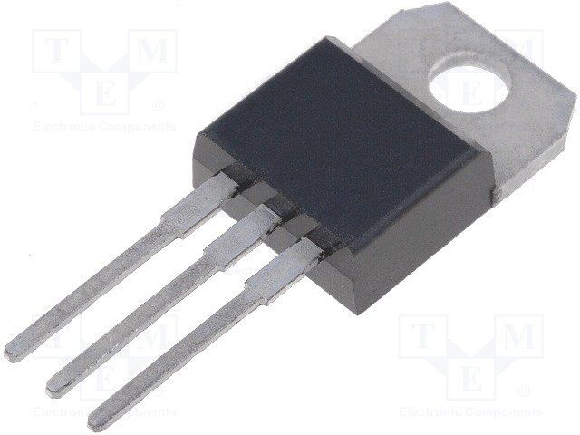
| 描述 | TRIAC ALTERNISTOR 600V TO220AB双向可控硅 6 Amp 600 Volt |
| 产品分类 | 双向可控硅分离式半导体 |
| GateTriggerCurrent-Igt | 50 mA |
| GateTriggerVoltage-Vgt | 1.3 V |
| 品牌 | STMicroelectronics |
| 产品手册 | |
| 产品图片 |
|
| rohs | 符合RoHS含铅 / 不符合限制有害物质指令(RoHS)规范要求 |
| 产品系列 | 晶体闸流管,双向可控硅,STMicroelectronics BTB06-600BWRGSnubberless™ |
| 数据手册 | |
| 产品型号 | BTB06-600BWRG |
| 三端双向可控硅类型 | 可控硅 - 无缓冲器 |
| 不重复通态电流 | 63 A |
| 产品培训模块 | http://www.digikey.cn/PTM/IndividualPTM.page?site=cn&lang=zhs&ptm=26297http://www.digikey.cn/PTM/IndividualPTM.page?site=cn&lang=zhs&ptm=26298 |
| 产品目录页面 | |
| 产品种类 | 双向可控硅 |
| 供应商器件封装 | TO-220AB |
| 保持电流Ih最大值 | 50 mA |
| 关闭状态漏泄电流(在VDRMIDRM下) | 5 uA |
| 其它名称 | 497-3391-5 |
| 其它有关文件 | http://www.st.com/web/catalog/sense_power/FM144/CL1221/SC124/PF76121?referrer=70071840 |
| 包装 | 管件 |
| 商标 | STMicroelectronics |
| 安装类型 | 通孔 |
| 安装风格 | Through Hole |
| 封装 | Tube |
| 封装/外壳 | TO-220-3 |
| 封装/箱体 | TO-220-3 |
| 工厂包装数量 | 50 |
| 开启状态电压 | 1.55 V |
| 最大工作温度 | + 125 C |
| 最大转折电流IBO | 63 A |
| 最小工作温度 | - 40 C |
| 栅极触发电压-Vgt | 1.3 V |
| 栅极触发电流-Igt | 50 mA |
| 标准包装 | 50 |
| 电压-断态 | 600V |
| 电压-栅极触发(Vgt)(最大值) | 1.3V |
| 电流-不重复浪涌50、60Hz(Itsm) | 60A,63A |
| 电流-保持(Ih)(最大值) | 50mA |
| 电流-栅极触发(Igt)(最大值) | 50mA |
| 电流-通态(It(RMS))(最大值) | 6A |
| 系列 | BTB06 |
| 配置 | 单一 |
| 额定重复关闭状态电压VDRM | 600 V |


- 商务部:美国ITC正式对集成电路等产品启动337调查
- 曝三星4nm工艺存在良率问题 高通将骁龙8 Gen1或转产台积电
- 太阳诱电将投资9.5亿元在常州建新厂生产MLCC 预计2023年完工
- 英特尔发布欧洲新工厂建设计划 深化IDM 2.0 战略
- 台积电先进制程称霸业界 有大客户加持明年业绩稳了
- 达到5530亿美元!SIA预计今年全球半导体销售额将创下新高
- 英特尔拟将自动驾驶子公司Mobileye上市 估值或超500亿美元
- 三星加码芯片和SET,合并消费电子和移动部门,撤换高东真等 CEO
- 三星电子宣布重大人事变动 还合并消费电子和移动部门
- 海关总署:前11个月进口集成电路产品价值2.52万亿元 增长14.8%


PDF Datasheet 数据手册内容提取
BTA06 and BTB06 Series ® 6A TRIACS SNUBBERLESS™, LOGIC LEVEL & STANDARD Table 1: Main Features A2 Symbol Value Unit I 6 A T(RMS) G VDRM/VRRM 600 and 800 V A1 I 5 to 50 mA GT (Q ) 1 A2 DESCRIPTION Available either in through-hole or surface-mount packages, the BTA06 and BTB06 triac series is A1 A1 suitable for general purpose AC switching. They A2G A2G can be used as an ON/OFF function in applica- TO-220AB Insulated TO-220AB tions such as static relays, heating regulation, in- (BTA06) (BTB06) duction motor starting circuits... or for phase control operation in light dimmers, motor speed controllers,... Table 2: Order Codes The snubberless and logic level versions (BTA/ Part Number Marking BTB...W) are specially recommended for use on BTA06-xxxxxRG See page table 8 on inductive loads, thanks to their high commutation BTB06-xxxxxRG page 6 performances. By using an internal ceramic pad, the BTA series provides voltage insulated tab (rated at 2500V ) complying with UL standards (File ref.: RMS E81734). Table 3: Absolute Maximum Ratings Symbol Parameter Value Unit TO-220AB T = 110°C RMS on-state current (full sine c I 6 A T(RMS) wave) TO-220AB Ins. T = 105°C c Non repetitive surge peak on-state F = 50 Hz t = 20 ms 60 I A TSM current (full cycle, T initial = 25°C) j F = 60 Hz t = 16.7 ms 63 I²t I²t Value for fusing tp = 10 ms 21 A²s Critical rate of rise of on-state cur- dI/dt rent I = 2 x I , t ≤ 100 ns F = 120 Hz Tj = 125°C 50 A/µs G GT r I Peak gate current t = 20 µs T = 125°C 4 A GM p j P Average gate power dissipation T = 125°C 1 W G(AV) j Tstg Storage junction temperature range - 40 to + 150 °C T Operating junction temperature range - 40 to + 125 j February 2006 REV. 6 1/7
BTA06 and BTB06 Series Tables 4: Electrical Characteristics (T = 25°C, unless otherwise specified) j ■ SNUBBERLESS and Logic Level (3 quadrants) BTA06 / BTB06 Symbol Test Conditions Quadrant Unit TW SW CW BW I (1) I - II - III MAX. 5 10 35 50 mA GT V = 12 V R = 30 Ω D L V I - II - III MAX. 1.3 V GT V = V R = 3.3 kΩ V D DRM L I - II - III MIN. 0.2 V GD T = 125°C j I (2) I = 100 mA MAX. 10 15 35 50 mA H T I - III 10 25 50 70 I I = 1.2 I MAX. mA L G GT II 15 30 60 80 dV/dt (2) V = 67 %V gate open T = 125°C MIN. 20 40 400 1000 V/µs D DRM j (dV/dt)c = 0.1 V/µs T = 125°C 2.7 3.5 - - j (dI/dt)c (2) (dV/dt)c = 10 V/µs T = 125°C MIN. 1.2 2.4 - - A/ms j Without snubber T = 125°C - - 3.5 5.3 j ■ Standard (4 quadrants) BTA06 / BTB06 Symbol Test Conditions Quadrant Unit C B I - II - III 25 50 I (1) MAX. mA GT V = 12 V R = 30 Ω IV 50 100 D L V ALL MAX. 1.3 V GT V V = V R = 3.3 kΩ T = 125°C ALL MIN. 0.2 V GD D DRM L j I (2) I = 500 mA MAX. 25 50 mA H T I - III - IV 40 50 I I = 1.2 I MAX. mA L G GT II 80 100 dV/dt (2) V = 67 %V gate open T = 125°C MIN. 200 400 V/µs D DRM j (dV/dt)c (2) (dI/dt)c = 2.7 A/ms T = 125°C MIN. 5 10 V/µs j Table 5: Static Characteristics Symbol Test Conditions Value Unit V (2) I = 8.5 A t = 380 µs T = 25°C MAX. 1.55 V TM TM p j V (2) Threshold voltage T = 125°C MAX. 0.85 V t0 j R (2) Dynamic resistance T = 125°C MAX. 60 mΩ d j IDRM Tj = 25°C 5 µA V = V MAX. IRRM DRM RRM Tj = 125°C 1 mA Note 1: minimum IGT is guaranted at 5% of IGT max. Note 2: for both polarities of A2 referenced to A1. 2/7
BTA06 and BTB06 Series Table 6: Thermal resistance Symbol Parameter Value Unit TO-220AB 1.8 R Junction to case (AC) °C/W th(j-c) TO-220AB Insulated 2.7 TO-220AB R Junction to ambient 60 °C/W th(j-a) TO-220AB Insulated Figure 1: Maximum power dissipation versus Figure 2: RMS on-state current versus case RMS on-state current (full cycle) temperature (full cycle) P(W) IT(RMS)(A) 8 7 BTB 7 6 6 BTA 5 5 4 4 3 3 2 2 1 1 IT(RMS)(A) TC(°C) 0 0 0 1 2 3 4 5 6 0 25 50 75 100 125 Figure 3: Relative variation of thermal Figure 4: On-state characteristics (maximum impedance versus pulse duration values) K=[Zth/Rth] ITM(A) 1E+0 100 Zth(j-c) Vt0Tj=m 0a.8x5.V Tj=Tjmax. Rd= 60 mΩ Zth(j-a) 1E-1 10 tp(s) VTM(V) 1E-2 1 1E-3 1E-2 1E-1 1E+0 1E+1 1E+2 5E+2 0.5 1.0 1.5 2.0 2.5 3.0 3.5 4.0 4.5 5.0 3/7
BTA06 and BTB06 Series Figure 5: Surge peak on-state current versus Figure 6: Non-repetitive surge peak on-state number of cycles current for a sinusoidal pulse with width t < 10 ms p and corresponding value of I2t ITSM(A) ITSM(A),I 2t (A 2s) 70 1000 Tjinitial=25°C 60 t=20ms 50 One cycle dI/dt limitation: 50A/µs 40 Non repetitive Tjinitial=25°C ITSM 100 30 Repetitive 20 TC=105°C I 2t 10 Number of cycles tp(ms) 0 10 1 10 100 1000 0.01 0.10 1.00 10.00 Figure 7: Relative variation of gate trigger Figure 8: Relative variation of critical rate of current, holding current and latching current decrease of main current versus (dV/dt)c versus junction temperature (typical values) (typical values) (Snubberless & logic level types) IGT,IH,IL[Tj] /IGT,IH,IL[Tj=25°C] (dI/dt)c [(dV/dt)c] / Specified (dI/dt)c 2.5 2.4 2.2 2.0 2.0 1.8 IGT 1.6 1.5 1.4 TW 1.2 BW/CW 1.0 IH& IL 1.0 SW 0.8 0.6 0.5 0.4 Tj(°C) 0.2 (dV/dt)c (V/µs) 0.0 0.0 -40 -20 0 20 40 60 80 100 120 140 0.1 1.0 10.0 100.0 Figure 9: Relative variation of critical rate of Figure 10: Relative variation of critical rate of decrease of main current versus (dV/dt)c decrease of main current versus junction (typical values) (Standard types) temperature (dI/dt)c [(dV/dt)c] / Specified (dI/dt)c (dI/dt)c [Tj] /(dI/dt)c [Tjspecified] 2.0 6 1.8 5 1.6 C 1.4 4 1.2 B 1.0 3 0.8 2 0.6 0.4 1 0.2 (dV/dt)c (V/µs) Tj(°C) 0.0 0 0.1 1.0 10.0 100.0 0 25 50 75 100 125 4/7
BTA06 and BTB06 Series Figure 11: Ordering Information Scheme BT A 06 - 600 BW (RG) Triac series Insulation A = insulated B = non insulated Current 06 = 6A Voltage 600 = 600V 800 = 800V Sensitivity and type B = 50mA Standard BW = 50mA Snubberless C = 25mA Standard CW = 35mASnubberless SW = 10mA Logic Level TW = 5mA Logic Level Packing mode RG =Tube Table 7: Product Selector Voltage (xxx) Part Number Sensitivity Type 600 V 800 V Package BTA/BTB06-xxxB X X 50 mA Standard TO-220AB BTA/BTB06-xxxBW X X 50 mA Snubberless TO-220AB BTA/BTB06-xxxC X X 25 mA Standard TO-220AB BTA/BTB06-xxxCW X X 35 mA Snubberless TO-220AB BTA/BTB06-xxxSW X X 10 mA Logic level TO-220AB BTA/BTB06-xxxTW X X 5 mA Logic Level TO-220AB BTB: non insulated TO-220AB package 5/7
BTA06 and BTB06 Series Figure 12: TO-220AB (insulated and non insulated) Package Mechanical Data DIMENSIONS REF. Millimeters Inches Min. Typ. Max. Min. Typ. Max. A 15.20 15.90 0.598 0.625 B C a1 3.75 0.147 Ø I b2 a2 13.00 14.00 0.511 0.551 L B 10.00 10.40 0.393 0.409 F b1 0.61 0.88 0.024 0.034 A b2 1.23 1.32 0.048 0.051 I4 C 4.40 4.60 0.173 0.181 l3 c1 0.49 0.70 0.019 0.027 a1 c2 c2 2.40 2.72 0.094 0.107 l2 e 2.40 2.70 0.094 0.106 a2 F 6.20 6.60 0.244 0.259 ØI 3.75 3.85 0.147 0.151 M b1 c1 I4 15.80 16.40 16.80 0.622 0.646 0.661 e L 2.65 2.95 0.104 0.116 l2 1.14 1.70 0.044 0.066 l3 1.14 1.70 0.044 0.066 M 2.60 0.102 In order to meet environmental requirements, ST offers these devices in ECOPACK® packages. These packages have a Lead-free second level interconnect . The category of second level interconnect is marked on the package and on the inner box label, in compliance with JEDEC Standard JESD97. The maximum ratings related to soldering conditions are also marked on the inner box label. ECOPACK is an ST trademark. ECOPACK specifications are available at: www.st.com. Table 8: Ordering Information Ordering type Marking Package Weight Base qty Delivery mode BTA/BTB06-xxxyzRG BTA/BTB06-xxxyz TO-220AB 2.3 g 50 Tube Note: xxx = voltage, yy = sensitivity, z = type Table 9: Revision History Date Revision Description of Changes Apr-2002 5A Last update. TO-220AB delivery mode changed from bulk to tube. 13-Feb-2006 6 ECOPACK statement added. 6/7
BTA06 and BTB06 Series Information furnished is believed to be accurate and reliable. However, STMicroelectronics assumes no responsibility for the consequences of use of such information nor for any infringement of patents or other rights of third parties which may result from its use. No license is granted by implication or otherwise under any patent or patent rights of STMicroelectronics. Specifications mentioned in this publication are subject to change without notice. This publication supersedes and replaces all information previously supplied. STMicroelectronics products are not authorized for use as critical components in life support devices or systems without express written approval of STMicroelectronics. The ST logo is a registered trademark of STMicroelectronics. All other names are the property of their respective owners © 2006 STMicroelectronics - All rights reserved STMicroelectronics group of companies Australia - Belgium - Brazil - Canada - China - Czech Republic - Finland - France - Germany - Hong Kong - India - Israel - Italy - Japan - Malaysia - Malta - Morocco - Singapore - Spain - Sweden - Switzerland - United Kingdom - United States of America www.st.com 7/7