ICGOO在线商城 > BSZ900N15NS3 G
 Datasheet下载
- 型号: BSZ900N15NS3 G
- 制造商: Infineon
- 库位|库存: xxxx|xxxx
- 要求:
| 数量阶梯 | 香港交货 | 国内含税 |
| +xxxx | $xxxx | ¥xxxx |
查看当月历史价格
查看今年历史价格
BSZ900N15NS3 G产品简介:
ICGOO电子元器件商城为您提供BSZ900N15NS3 G由Infineon设计生产,在icgoo商城现货销售,并且可以通过原厂、代理商等渠道进行代购。 提供BSZ900N15NS3 G价格参考以及InfineonBSZ900N15NS3 G封装/规格参数等产品信息。 你可以下载BSZ900N15NS3 G参考资料、Datasheet数据手册功能说明书, 资料中有BSZ900N15NS3 G详细功能的应用电路图电压和使用方法及教程。
| 参数 | 数值 |
| 产品目录 | |
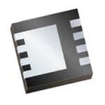
| 描述 | MOSFET N-CH 150V 13A TDSON-8 |
| 产品分类 | FET - 单 |
| FET功能 | 标准 |
| FET类型 | MOSFET N 通道,金属氧化物 |
| 品牌 | Infineon Technologies |
| 数据手册 | http://www.infineon.com/dgdl/BSZ900N15NS3+Rev2.1.pdf?folderId=db3a304326623792012669f6bee2224b&fileId=db3a304326623792012669f7decc224c |
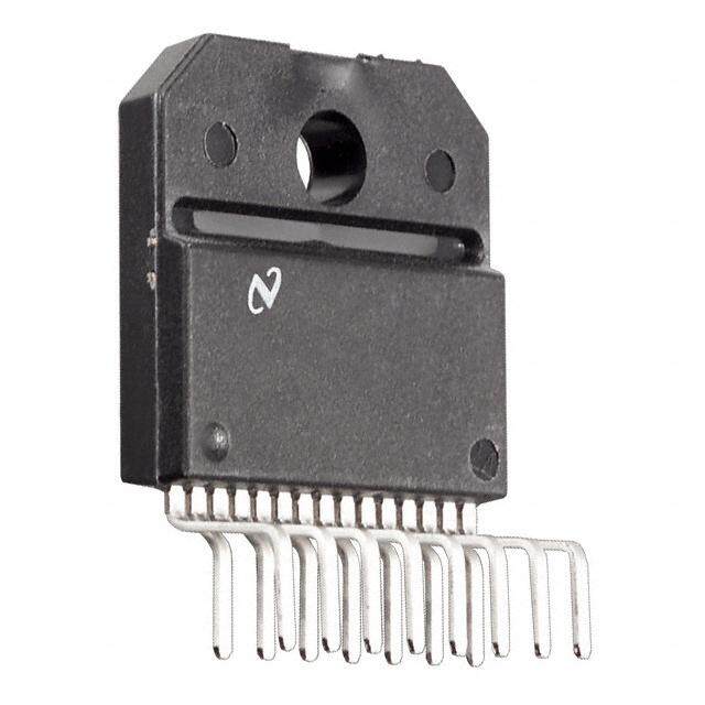
| 产品图片 |
|
| 产品型号 | BSZ900N15NS3 G |
| PCN其它 | |
| rohs | 无铅 / 符合限制有害物质指令(RoHS)规范要求 |
| 产品系列 | OptiMOS™ |
| 不同Id时的Vgs(th)(最大值) | 4V @ 20µA |
| 不同Vds时的输入电容(Ciss) | 510pF @ 75V |
| 不同Vgs时的栅极电荷(Qg) | 7nC @ 10V |
| 不同 Id、Vgs时的 RdsOn(最大值) | 90 毫欧 @ 10A,10V |
| 供应商器件封装 | PG-TSDSON-8(3.3x3.3) |
| 其它名称 | BSZ900N15NS3 GDKR |
| 功率-最大值 | 38W |
| 包装 | Digi-Reel® |
| 安装类型 | 表面贴装 |
| 封装/外壳 | 8-PowerTDFN |
| 标准包装 | 1 |
| 漏源极电压(Vdss) | 150V |
| 电流-连续漏极(Id)(25°C时) | 13A (Tc) |


- 商务部:美国ITC正式对集成电路等产品启动337调查
- 曝三星4nm工艺存在良率问题 高通将骁龙8 Gen1或转产台积电
- 太阳诱电将投资9.5亿元在常州建新厂生产MLCC 预计2023年完工
- 英特尔发布欧洲新工厂建设计划 深化IDM 2.0 战略
- 台积电先进制程称霸业界 有大客户加持明年业绩稳了
- 达到5530亿美元!SIA预计今年全球半导体销售额将创下新高
- 英特尔拟将自动驾驶子公司Mobileye上市 估值或超500亿美元
- 三星加码芯片和SET,合并消费电子和移动部门,撤换高东真等 CEO
- 三星电子宣布重大人事变动 还合并消费电子和移动部门
- 海关总署:前11个月进口集成电路产品价值2.52万亿元 增长14.8%


PDF Datasheet 数据手册内容提取
s BSZ900N15NS3 G OptiMOSTM3 Power-Transistor Product Summary Package V 150 V DS Marking R 90 mΩ DS(on),max • N-channel, normal level I 13 A D • Excellent gate charge x R product (FOM) DS(on) • Very low on-resistance R DS(on) PG-TSDSON-8 • 150 °C operating temperature • Pb-free lead plating; RoHS compliant • Qualified according to JEDEC1) for target application • Halogen-free according to IEC61249-2-21 Type Package Marking BSZ900N15NS3 G PG-TSDSON-8 900N15N Maximum ratings, at T=25 °C, unless otherwise specified j Parameter Symbol Conditions Value Unit Continuous drain current I T =25 °C 13 A D C T =100 °C 8 C Pulsed drain current2) ID,pulse TC=25 °C 52 Avalanche energy, single pulse E I =10 A, R =25 Ω 30 mJ AS D GS Gate source voltage V ±20 V GS Power dissipation P T =25 °C 38 W tot C Operating and storage temperature T, T -55 ... 150 °C j stg IEC climatic category; DIN IEC 68-1 55/150/56 1)J-STD20 and JESD22 Rev. 2.1 page 1 2011-05-16
BSZ900N15NS3 G Parameter Symbol Conditions Values Unit min. typ. max. Thermal characteristics Thermal resistance, junction - case R - - 3.3 K/W thJC Thermal resistance, junction - ambient RthJA 6 cm2 cooling area3) - - 60 Electrical characteristics, at T=25 °C, unless otherwise specified j Static characteristics Drain-source breakdown voltage V V =0 V, I =1 mA 150 - - V (BR)DSS GS D Gate threshold voltage V V =V , I =20 µA 2 3 4 GS(th) DS GS D V =120 V, V =0 V, Zero gate voltage drain current I DS GS - 0.01 1 µA DSS T=25 °C j V =120 V, V =0 V, DS GS - 10 100 T=125 °C j Gate-source leakage current I V =20 V, V =0 V - 1 100 nA GSS GS DS Drain-source on-state resistance R V =10 V, I =10 A - 74 90 mΩ DS(on) GS D V =8 V, I =5 A - 75 91 GS D Gate resistance R - 1.7 - Ω G |V |>2|I |R , Transconductance g DS D DS(on)max 6 12 - S fs I =10 A D 3) see figure 3 Rev. 2.1 page 2 2011-05-16
BSZ900N15NS3 G Parameter Symbol Conditions Values Unit min. typ. max. Dynamic characteristics Input capacitance C - 380 510 pF iss V =0 V, V =75 V, Output capacitance C GS DS - 46 61 oss f=1 MHz Reverse transfer capacitance C - 3 - rss Turn-on delay time t - 4 - ns d(on) Rise time tr V =75 V, V =10 V, - 4 - DD GS I =5 A, R =1.6 Ω Turn-off delay time t D G - 8 - d(off) Fall time t - 3 - f Gate Charge Characteristics4) Gate to source charge Q - 1.9 - nC gs Gate to drain charge Q - 0.9 - gd V =75 V, I =5 A, Switching charge Q DD D - 1.7 - sw V =0 to 10 V GS Gate charge total Q - 5.0 7 g Gate plateau voltage V - 5.2 - V plateau Output charge Q V =75 V, V =0 V - 12 17 nC oss DD GS Reverse Diode Diode continous forward current I - - 13 A S T =25 °C C Diode pulse current I - - 52 S,pulse V =0 V, I =13 A, Diode forward voltage V GS F - 0.9 1.2 V SD T=25 °C j Reverse recovery time trr V =75 V, I =5 A, - 59 ns R F di /dt=100 A/µs Reverse recovery charge Q F - 123 - nC rr 4) See figure 16 for gate charge parameter definition Rev. 2.1 page 3 2011-05-16
BSZ900N15NS3 G 1 Power dissipation 2 Drain current P =f(T ) I =f(T ); V ≥10 V tot C D C GS 40 15 35 30 10 25 [W]tot 20 [A]D P I 15 5 10 5 0 0 0 40 80 120 160 0 40 80 120 160 TC [°C] T [°C] C 3 Safe operating area 4 Max. transient thermal impedance I =f(V ); T =25 °C; D=0 Z =f(t ) D DS C thJC p parameter: t parameter: D=t /T p p 102 101 1 µs 10 µs 101 100 µs 0.5 W] A] 1 ms K/ [D [C 100 0.2 I hJ t Z DC 0.1 100 0.05 0.02 0.01 single pulse 10-1 10-1 10-1 100 101 102 103 V [V] t [s] DS p Rev. 2.1 page 4 2011-05-16
BSZ900N15NS3 G 5 Typ. output characteristics 6 Typ. drain-source on resistance I =f(V ); T=25 °C R =f(I ); T=25 °C D DS j DS(on) D j parameter: V parameter: V GS GS 30 150 140 130 5 V 5.5 V 25 10 V 120 6 V 110 20 7 V 100 ] 90 Ω 8 V m [A]D 15 [on) 7800 10 V I 6 V S( D R 60 10 50 40 5.5 V 30 5 20 5 V 10 4.5 V 0 0 0 1 2 3 0 4 8 12 16 V [V] I [A] DS D 7 Typ. transfer characteristics 8 Typ. forward transconductance I =f(V ); |V |>2|I |R g =f(I ); T=25 °C D GS DS D DS(on)max fs D j parameter: T j 28 20 24 15 20 16 A] S] I [D g [fs 10 12 8 5 4 150 °C 25 °C 0 0 0 2 4 6 8 0 10 20 30 V [V] I [A] GS D Rev. 2.1 page 5 2011-05-16
BSZ900N15NS3 G 9 Drain-source on-state resistance 10 Typ. gate threshold voltage R =f(T); I =10 A; V =10 V V =f(T); V =V DS(on) j D GS GS(th) j GS DS parameter: I D 200 4 180 3.5 160 200 µA 3 140 20 µA 2.5 ]Ω 120 m 98 % V] R [DS(on) 10800 typ V [GS(th) 2 1.5 60 1 40 0.5 20 0 0 -60 -20 20 60 100 140 180 -60 -20 20 60 100 140 180 T [°C] T [°C] j j 11 Typ. capacitances 12 Forward characteristics of reverse diode C=f(V ); V =0 V; f=1 MHz I =f(V ) DS GS F SD parameter: T j 103 100 Ciss 102 25 °C Coss 150 °C, 98% C [pF] I [A]F 10 150 °C 101 25 °C, 98% Crss 100 1 0 20 40 60 80 100 0 0.5 1 1.5 2 V [V] V [V] DS SD Rev. 2.1 page 6 2011-05-16
BSZ900N15NS3 G 13 Avalanche characteristics 14 Typ. gate charge I =f(t ); R =25 Ω V =f(Q ); I =5 A pulsed AS AV GS GS gate D parameter: T parameter: V j(start) DD 100 10 120 V 8 75 V 30 V 6 A] V] [AS 10 [GS I V 4 25 °C 100 °C 2 125 °C 1 0 1 10 100 1000 0 2 4 6 t [µs] Q [nC] AV gate 15 Drain-source breakdown voltage 16 Gate charge waveforms V =f(T); I =1 mA BR(DSS) j D 170 V GS 165 Qg 160 V] 155 [S) S D R( B 150 V V gs(th) 145 140 Qg(th) Qsw Qgate Q Q 135 gs gd -60 -20 20 60 100 140 180 T [°C] j Rev. 2.1 page 7 2011-05-16
BSZ900N15NS3 G Package Outline: PG-TSDSON-8 Rev. 2.1 page 8 2011-05-16
BSZ900N15NS3 G Published by Infineon Technologies AG 81726 Munich, Germany © 2009 Infineon Technologies AG All Rights Reserved. Legal Disclaimer The information given in this document shall in no event be regarded as a guarantee of conditions or characteristics. With respect to any examples or hints given herein, any typical values stated herein and/or any information regarding the application of the device, Infineon Technologies hereby disclaims any and all warranties and liabilities of any kind, including without limitation, warranties of non-infringement of intellectual property rights of any third party. Information For further information on technology, delivery terms and conditions and prices, please contact the nearest Infineon Technologies Office (www.infineon.com). Warnings Due to technical requirements, components may contain dangerous substances. For information on the types in question, please contact the nearest Infineon Technologies Office. Infineon Technologies components may be used in life-support devices or systems only with the express written approval of Infineon Technologies, if a failure of such components can reasonably be expected to cause the failure of that life-support device or system or to affect the safety or effectiveness of that device or system. Life support devices or systems are intended to be implanted in the human body or to support and/or maintain and sustain Rev. 2.1 page 9 2011-05-16
Mouser Electronics Authorized Distributor Click to View Pricing, Inventory, Delivery & Lifecycle Information: I nfineon: BSZ900N15NS3 G BSZ900N15NS3GATMA1