ICGOO在线商城 > 分立半导体产品 > 晶体管 - FET,MOSFET - 单 > BSP130,115

 Datasheet下载
- 型号: BSP130,115
- 制造商: NXP Semiconductors
- 库位|库存: xxxx|xxxx
- 要求:
| 数量阶梯 | 香港交货 | 国内含税 |
| +xxxx | $xxxx | ¥xxxx |
查看当月历史价格
查看今年历史价格
BSP130,115产品简介:
ICGOO电子元器件商城为您提供BSP130,115由NXP Semiconductors设计生产,在icgoo商城现货销售,并且可以通过原厂、代理商等渠道进行代购。 BSP130,115价格参考¥1.62-¥1.62。NXP SemiconductorsBSP130,115封装/规格:晶体管 - FET,MOSFET - 单, 表面贴装 N 沟道 300V 350mA(Ta) 1.5W(Ta) SOT-223。您可以下载BSP130,115参考资料、Datasheet数据手册功能说明书,资料中有BSP130,115 详细功能的应用电路图电压和使用方法及教程。
| 参数 | 数值 |
| 产品目录 | |
| 描述 | MOSFET N-CH 300V 350MA SC73MOSFET TAPE-7 MOSFET |
| 产品分类 | FET - 单分离式半导体 |
| FET功能 | 逻辑电平门 |
| FET类型 | MOSFET N 通道,金属氧化物 |
| Id-连续漏极电流 | 350 mA |
| 品牌 | NXP Semiconductors |
| 产品手册 | |
| 产品图片 |
|
| rohs | 符合RoHS无铅 / 符合限制有害物质指令(RoHS)规范要求 |
| 产品系列 | 晶体管,MOSFET,NXP Semiconductors BSP130,115- |
| 数据手册 | |
| 产品型号 | BSP130,115 |
| PCN封装 | |
| PCN设计/规格 | |
| Pd-PowerDissipation | 1.5 W |
| Pd-功率耗散 | 1.5 W |
| RdsOn-漏源导通电阻 | 6 Ohms |
| Vds-漏源极击穿电压 | 300 V |
| Vgs-Gate-SourceBreakdownVoltage | +/- 20 V |
| Vgs-栅源极击穿电压 | 20 V |
| 不同Id时的Vgs(th)(最大值) | 2V @ 1mA |
| 不同Vds时的输入电容(Ciss) | 120pF @ 25V |
| 不同Vgs时的栅极电荷(Qg) | - |
| 不同 Id、Vgs时的 RdsOn(最大值) | 6 欧姆 @ 250mA,10V |
| 产品种类 | MOSFET |
| 供应商器件封装 | SC-73 |
| 其它名称 | 568-6220-6 |
| 功率-最大值 | 1.5W |
| 包装 | Digi-Reel® |
| 商标 | NXP Semiconductors |
| 安装类型 | 表面贴装 |
| 安装风格 | SMD/SMT |
| 导通电阻 | 6 Ohms |
| 封装 | Reel |
| 封装/外壳 | TO-261-4,TO-261AA |
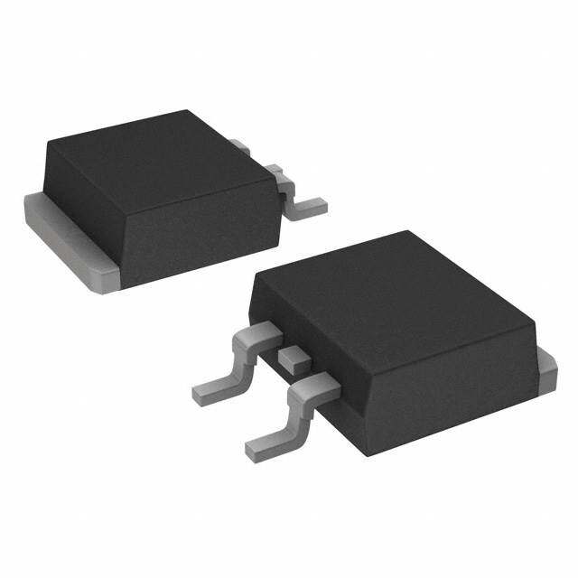
| 封装/箱体 | SOT-223-3 |
| 工厂包装数量 | 1000 |
| 晶体管极性 | N-Channel |
| 最大工作温度 | + 150 C |
| 最小工作温度 | - 55 C |
| 标准包装 | 1 |
| 汲极/源极击穿电压 | 300 V |
| 漏极连续电流 | 350 mA |
| 漏源极电压(Vdss) | 300V |
| 电流-连续漏极(Id)(25°C时) | 350mA (Ta) |
| 通道模式 | Enhancement |
| 配置 | Single Dual Drain |
| 零件号别名 | BSP130 T/R |

SOT223-1.jpg)


.jpg)


- 商务部:美国ITC正式对集成电路等产品启动337调查
- 曝三星4nm工艺存在良率问题 高通将骁龙8 Gen1或转产台积电
- 太阳诱电将投资9.5亿元在常州建新厂生产MLCC 预计2023年完工
- 英特尔发布欧洲新工厂建设计划 深化IDM 2.0 战略
- 台积电先进制程称霸业界 有大客户加持明年业绩稳了
- 达到5530亿美元!SIA预计今年全球半导体销售额将创下新高
- 英特尔拟将自动驾驶子公司Mobileye上市 估值或超500亿美元
- 三星加码芯片和SET,合并消费电子和移动部门,撤换高东真等 CEO
- 三星电子宣布重大人事变动 还合并消费电子和移动部门
- 海关总署:前11个月进口集成电路产品价值2.52万亿元 增长14.8%


PDF Datasheet 数据手册内容提取
Important notice Dear Customer, On 7 February 2017 the former NXP Standard Product business became a new company with the tradename Nexperia. Nexperia is an industry leading supplier of Discrete, Logic and PowerMOS semiconductors with its focus on the automotive, industrial, computing, consumer and wearable application markets In data sheets and application notes which still contain NXP or Philips Semiconductors references, use the references to Nexperia, as shown below. Instead of http://www.nxp.com, http://www.philips.com/ or http://www.semiconductors.philips.com/, use http://www.nexperia.com Instead of sales.addresses@www.nxp.com or sales.addresses@www.semiconductors.philips.com, use salesaddresses@nexperia.com (email) Replace the copyright notice at the bottom of each page or elsewhere in the document, depending on the version, as shown below: - © NXP N.V. (year). All rights reserved or © Koninklijke Philips Electronics N.V. (year). All rights reserved Should be replaced with: - © Nexperia B.V. (year). All rights reserved. If you have any questions related to the data sheet, please contact our nearest sales office via e-mail or telephone (details via salesaddresses@nexperia.com). Thank you for your cooperation and understanding, Kind regards, Team Nexperia
DISCRETE SEMICONDUCTORS DATA SHEET age M3D087 BSP130 N-channel enhancement mode vertical D-MOS transistor Product specification 2001 Dec 11 Supersedes data of 1997 Jun 23
Philips Semiconductors Product specification N-channel enhancement mode BSP130 vertical D-MOS transistor FEATURES PINNING - SOT223 • Direct interface to C-MOS, TTL, etc. PIN DESCRIPTION • High-speed switching 1 gate • No secondary breakdown. 2 drain 3 source APPLICATIONS 4 drain • Line current interruptor in telephone sets • Relay, high-speed and line transformer drivers. handbook, halfpage 4 d DESCRIPTION N-channel enhancement mode vertical D-MOS transistor g in a SOT223 package. 1 2 3 s Top view MAM054 Marking codeBSP130. Fig.1 Simplified outline and symbol. QUICK REFERENCE DATA SYMBOL PARAMETER CONDITIONS MIN. MAX. UNIT V drain-source voltage (DC) - 300 V DS I drain current (DC) - 350 mA D P total power dissipation T £ 25(cid:176) C - 1.5 W tot amb V gate-source voltage open drain - – 20 V GSO R drain-source on-state I =250mA; V =10V - 6 W DSon D GS resistance V gate-source cut-off voltage I =1mA; V =V 0.8 2 V GSoff D DS GS LIMITING VALUES In accordance with the Absolute Maximum Rating System (IEC60134). SYMBOL PARAMETER CONDITIONS MIN. MAX. UNIT V drain-source voltage (DC) - 300 V DS V gate-source voltage (DC) open drain - – 20 V GSO I drain current (DC) - 350 mA D I peak drain current - 1.4 A DM P total power dissipation T £ 25(cid:176) C;note 1 - 1.5 W tot amb T storage temperature - 55 +150 (cid:176) C stg T junction temperature - 150 (cid:176) C j Note 1. Devicemountedonanepoxyprinted-circuitboard,40x40x1.5mm,mountingpadforthedraintabminimum6cm2. 2001Dec11 2
Philips Semiconductors Product specification N-channel enhancement mode BSP130 vertical D-MOS transistor THERMAL CHARACTERISTICS SYMBOL PARAMETER VALUE UNIT R thermal resistance from junction to ambient; note 1 83.3 K/W th j-a Note 1. Devicemountedonanepoxyprinted-circuitboard,40x40x1.5mm,mountingpadforthedraintabminimum6cm2. STATIC CHARACTERISTICS T = 25(cid:176) C unless otherwise specified. j SYMBOL PARAMETER CONDITIONS MIN. TYP. MAX. UNIT V drain-source breakdown voltage I =10m A; V =0 300 - - V (BR)DSS D GS I gate-source leakage current V =– 20V; V =0 - - – 100 nA GSS GS DS V gate-source threshold voltage I =1mA; V =V 0.8 - 2 V GSth D DS GS R drain-source on-state resistance I =20mA; V =2.4V - 4.8 10 W DSon D GS I =250mA; V =10V - 3.7 6 W D GS I drain-source leakage current V =240V; V =0 - - 100 nA DSS DS GS (cid:247) Y (cid:247) transfer admittance I =250mA; V =25V 200 690 - mS fs D DS C input capacitance V =25V; V =0; f=1MHz - 100 120 pF iss DS GS C output capacitance V =25V; V =0; f=1MHz - 21 30 pF oss DS GS C feedback capacitance V =25V; V =0; f=1MHz - 10 15 pF rss DS GS Switching times (see Figs2 and3) t turn-on time I =250mA;V =50V; - 6 10 ns on D DD V =0to10V GS t turn-off time I = 250mA;V = 50V; - 46 60 ns off D DD V =10 to 0V GS 2001Dec11 3
Philips Semiconductors Product specification N-channel enhancement mode BSP130 vertical D-MOS transistor handbook, halfpage 90 % handbook, halfpage VDD = 50 V INPUT 10 % 90 % 10 V OUTPUT ID 0 V 10 % 50 W ton toff MBB691 MBB692 Fig.2 Switching times test circuit. Fig.3 Input and output waveforms. MRC218 MLD765 2 250 handbook, halfpage handbook, halfpage Ptot C (pF) (W) 200 1.5 150 1 100 Ciss 0.5 50 Coss Crss 0 0 0 50 100 150 200 0 10 20 30 Tj ((cid:176)C) VDS (V) VGS=0; f=1MHz; Tj=25(cid:176)C. Fig.5 Capacitance as a function of drain-source Fig.4 Power derating curve. voltage; typical values. 2001Dec11 4
Philips Semiconductors Product specification N-channel enhancement mode BSP130 vertical D-MOS transistor MLD766 MLD767 1.2 1.2 handbook, halfpage VGS = 10 V 5 V handbook, halfpage ID 4 V ID (A) 3.5 V (A) 3 V 0.8 0.8 0.4 0.4 2.5 V 2 V 0 0 0 4 8 12 0 2 4 6 8 10 VDS (V) VGS (V) Tj=25(cid:176)C. VDS=10V; Tj=25(cid:176)C. Fig.6 Typical output characteristics. Fig.7 Typical transfer characteristics. MLD768 MLD769 30 20 handbook, halfpage VGS = 2 V handbook, halfpage 2.5 V RDSon RDSon 3 V 3.5 V (W ) (W ) 15 20 10 10 5 4 V 5 V 10 V 0 0 10- 1 1 10 0 2 4 6 8 10 ID (A) VGS (V) Tj=25(cid:176)C. VDS=100mV; Tj=25(cid:176)C. Fig.8 Drain-source on-state resistance as a Fig.9 Drain-sourceon-stateresistanceasafunction function of drain current; typical values. of gate-source voltage; typical values. 2001Dec11 5
Philips Semiconductors Product specification N-channel enhancement mode BSP130 vertical D-MOS transistor 102 MRC221 handbook, full pagewidd th= 0.75 Rth j-a 0.5 (K/W) 0.2 10 0.1 0.05 0.02 1 0.01 P d = tp T 0 tp t T 10- 1 10- 5 10- 4 10- 3 10- 2 10- 1 1 10 102 103 tp (s) Fig.10 Transient thermal resistance from junction to ambient as a function of pulse time. MLD773 10 handbook, halfpage ID (A) 1 (1) tp = 10 m s 100 m s 1 ms 10- 1 DC 10 ms 100 ms P d =tp T 1s 10- 2 tp t T 10- 3 1 10 102 103 VDS (V) d =0.01; Tamb=25(cid:176)C. (1) RDSon limitation. Fig.11 SOAR curve. 2001Dec11 6
Philips Semiconductors Product specification N-channel enhancement mode BSP130 vertical D-MOS transistor MLD771 MLD772 2 1.25 handbook, halfpage handbook, halfpage k k (1) 1 1.5 (2) 0.75 1 0.5 0.5 0.25 0 0 - 50 0 50 100 150 -50 0 50 100 150 Tj ((cid:176)C) Tj ((cid:176)C) R atT k = -R---------D---S---(-o---an--)-t-- -2----5-----(cid:176)--j-C--- Typical DRSD(oSno)n; k = -V----G-V---S-G--(--tS-h--(-)-t--h-a--)-t-- a-2---t-5 --T---(cid:176)-j--C---. (1) ID=250mA; VGS=10V. (2)ID=20mA; VGS=2.4V. Typical VGSth at 1mA. Fig.12 Temperature coefficient of drain-source Fig.13 Temperature coefficient of gate-source on-state resistance; typical values. threshold voltage; typical values. 2001Dec11 7
Philips Semiconductors Product specification N-channel enhancement mode BSP130 vertical D-MOS transistor PACKAGE OUTLINE Plastic surface mounted package; collector pad for good heat transfer; 4 leads SOT223 D B E A X c y HE v M A b1 4 Q A A1 1 2 3 Lp e1 bp w M B detail X e 0 2 4 mm scale DIMENSIONS (mm are the original dimensions) UNIT A A1 bp b1 c D E e e1 HE Lp Q v w y 1.8 0.10 0.80 3.1 0.32 6.7 3.7 7.3 1.1 0.95 mm 4.6 2.3 0.2 0.1 0.1 1.5 0.01 0.60 2.9 0.22 6.3 3.3 6.7 0.7 0.85 OUTLINE REFERENCES EUROPEAN ISSUE DATE VERSION IEC JEDEC EIAJ PROJECTION 97-02-28 SOT223 SC-73 99-09-13 2001Dec11 8
Philips Semiconductors Product specification N-channel enhancement mode BSP130 vertical D-MOS transistor DATA SHEET STATUS PRODUCT DATA SHEET STATUS(1) DEFINITIONS STATUS(2) Objective data Development This data sheet contains data from the objective specification for product development. Philips Semiconductors reserves the right to change the specification in any manner without notice. Preliminary data Qualification This data sheet contains data from the preliminary specification. Supplementary data will be published at a later date. Philips Semiconductors reserves the right to change the specification without notice, in order to improve the design and supply the best possible product. Product data Production This data sheet contains data from the product specification. Philips Semiconductors reserves the right to makechanges at any time in order to improve the design, manufacturing and supply. Changes will be communicatedaccording to the Customer Product/Process Change Notification (CPCN) procedure SNW-SQ-650A. Notes 1. Please consult the most recently issued data sheet before initiating or completing a design. 2. The product status of the device(s) described in this data sheet may have changed since this data sheet was published. The latest information is available on the Internet at URL http://www.semiconductors.philips.com. DEFINITIONS DISCLAIMERS Short-form specification(cid:190) The data in a short-form Life support applications(cid:190) These products are not specification is extracted from a full data sheet with the designed for use in life support appliances, devices, or same type number and title. For detailed information see systems where malfunction of these products can the relevant data sheet or data handbook. reasonablybeexpectedtoresultinpersonalinjury.Philips Semiconductorscustomersusingorsellingtheseproducts Limitingvaluesdefinition(cid:190) Limitingvaluesgivenarein for use in such applications do so at their own risk and accordance with the Absolute Maximum Rating System agree to fully indemnify Philips Semiconductors for any (IEC60134). Stress above one or more of the limiting damages resulting from such application. values may cause permanent damage to the device. These are stress ratings only and operation of the device Right to make changes(cid:190) Philips Semiconductors attheseoratanyotherconditionsabovethosegiveninthe reservestherighttomakechanges,withoutnotice,inthe Characteristicssectionsofthespecificationisnotimplied. products, including circuits, standard cells, and/or Exposure to limiting values for extended periods may software, described or contained herein in order to affect device reliability. improve design and/or performance. Philips Semiconductors assumes no responsibility or liability for Application information(cid:190) Applications that are theuseofanyoftheseproducts,conveysnolicenceortitle described herein for any of these products are for under any patent, copyright, or mask work right to these illustrative purposes only. Philips Semiconductors make products,andmakesnorepresentationsorwarrantiesthat norepresentationorwarrantythatsuchapplicationswillbe these products are free from patent, copyright, or mask suitable for the specified use without further testing or work right infringement, unless otherwise specified. modification. 2001Dec11 9
Philips Semiconductors Product specification N-channel enhancement mode BSP130 vertical D-MOS transistor NOTES 2001Dec11 10
Philips Semiconductors Product specification N-channel enhancement mode BSP130 vertical D-MOS transistor NOTES 2001Dec11 11
Philips Semiconductors – a worldwide company Contact information For additional information please visit http://www.semiconductors.philips.com. Fax:+31402724825 For sales offices addresses send e-mail to:sales.addresses@www.semiconductors.philips.com. © Koninklijke Philips Electronics N.V. 2001 SCA73 All rights are reserved. Reproduction in whole or in part is prohibited without the prior written consent of the copyright owner. Theinformationpresentedinthisdocumentdoesnotformpartofanyquotationorcontract,isbelievedtobeaccurateandreliableandmaybechanged without notice. No liability will be accepted by the publisher for any consequence of its use. Publication thereof does not convey nor imply any license under patent- or other industrial or intellectual property rights. Printed in The Netherlands 613510/03/pp12 Date of release:2001Dec11 Document order number: 939775009064
Mouser Electronics Authorized Distributor Click to View Pricing, Inventory, Delivery & Lifecycle Information: N experia: BSP130,115