ICGOO在线商城 > 分立半导体产品 > 晶体管 - FET,MOSFET - 单 > BS170G

 Datasheet下载
- 型号: BS170G
- 制造商: ON Semiconductor
- 库位|库存: xxxx|xxxx
- 要求:
| 数量阶梯 | 香港交货 | 国内含税 |
| +xxxx | $xxxx | ¥xxxx |
查看当月历史价格
查看今年历史价格
BS170G产品简介:
ICGOO电子元器件商城为您提供BS170G由ON Semiconductor设计生产,在icgoo商城现货销售,并且可以通过原厂、代理商等渠道进行代购。 BS170G价格参考。ON SemiconductorBS170G封装/规格:晶体管 - FET,MOSFET - 单, 通孔 N 沟道 60V 500mA(Ta) 350mW(Ta) TO-92-3。您可以下载BS170G参考资料、Datasheet数据手册功能说明书,资料中有BS170G 详细功能的应用电路图电压和使用方法及教程。
| 参数 | 数值 |
| 产品目录 | |
| ChannelMode | Enhancement |
| 描述 | MOSFET N-CH 60V 500MA TO-92MOSFET 60V 500mA N-Channel |
| 产品分类 | FET - 单分离式半导体 |
| FET功能 | 标准 |
| FET类型 | MOSFET N 通道,金属氧化物 |
| Id-ContinuousDrainCurrent | 500 mA |
| Id-连续漏极电流 | 500 mA |
| 品牌 | ON Semiconductor |
| 产品手册 | |
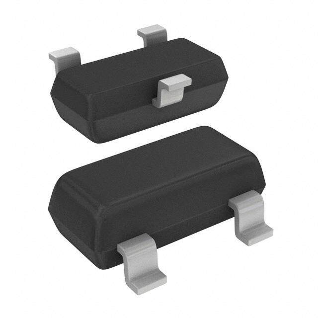
| 产品图片 |
|
| rohs | 符合RoHS无铅 / 符合限制有害物质指令(RoHS)规范要求 |
| 产品系列 | 晶体管,MOSFET,ON Semiconductor BS170G- |
| 数据手册 | |
| 产品型号 | BS170G |
| PCN组件/产地 | |
| PCN过时产品 | |
| Pd-PowerDissipation | 0.35 W |
| Pd-功率耗散 | 350 mW |
| RdsOn-Drain-SourceResistance | 5 Ohms |
| RdsOn-漏源导通电阻 | 5 Ohms |
| Vds-Drain-SourceBreakdownVoltage | 60 V |
| Vds-漏源极击穿电压 | 60 V |
| Vgs-Gate-SourceBreakdownVoltage | +/- 20 V |
| Vgs-栅源极击穿电压 | 20 V |
| 不同Id时的Vgs(th)(最大值) | 3V @ 1mA |
| 不同Vds时的输入电容(Ciss) | 60pF @ 10V |
| 不同Vgs时的栅极电荷(Qg) | - |
| 不同 Id、Vgs时的 RdsOn(最大值) | 5 欧姆 @ 200mA,10V |
| 产品目录页面 | |
| 产品种类 | MOSFET |
| 供应商器件封装 | TO-92-3 |
| 其它名称 | BS170G-ND |
| 功率-最大值 | 350mW |
| 功率耗散 | 0.35 W |
| 包装 | 管件 |
| 商标 | ON Semiconductor |
| 安装类型 | 通孔 |
| 安装风格 | Through Hole |
| 导通电阻 | 5 Ohms |
| 封装 | Bulk |
| 封装/外壳 | TO-226-3、TO-92-3 标准主体 |
| 封装/箱体 | TO-92-3 |
| 工厂包装数量 | 1000 |
| 晶体管极性 | N-Channel |
| 最大工作温度 | + 150 C |
| 最小工作温度 | - 55 C |
| 标准包装 | 1,000 |
| 正向跨导-最小值 | 0.2 S |
| 汲极/源极击穿电压 | 60 V |
| 漏极连续电流 | 500 mA |
| 漏源极电压(Vdss) | 60V |
| 电流-连续漏极(Id)(25°C时) | 500mA (Ta) |
| 系列 | BS170 |
| 通道模式 | Enhancement |
| 配置 | Single |
| 闸/源击穿电压 | +/- 20 V |

,TO-226_straightlead.jpg)


PDF Datasheet 数据手册内容提取
BS170 Small Signal MOSFET 500 mA, 60 Volts N−Channel TO−92 (TO−226) Features www.onsemi.com • This is a Pb−Free Device* 500 mA, 60 Volts MAXIMUM RATINGS Rating Symbol Value Unit RDS(on) = 5.0 (cid:3) Drain−Source Voltage VDS 60 Vdc N−Channel Gate−Source Voltage − Continuous VGS ±20 Vdc D − Non−repetitive (tp ≤ 50 (cid:2)s) VGSM ±40 Vpk Drain Current (Note) ID 0.5 Adc Total Device Dissipation @ TA = 25°C PD 350 mW G Operating and Storage Junction TJ, Tstg −55 to °C Temperature Range +150 S Stresses exceeding those listed in the Maximum Ratings table may damage the device. If any of these limits are exceeded, device functionality should not be assumed, damage may occur and reliability may be affected. NOTE:The Power Dissipation of the package may result in a lower continuous drain current. TO−92 (TO−226) CASE 29 *For additional information on our Pb−Free strategy and soldering details, please STYLE 30 download the ON Semiconductor Soldering and Mounting Techniques Reference Manual, SOLDERRM/D. 1 2 3 MARKING DIAGRAM & PIN ASSIGNMENT BS170 AYWW(cid:2) (cid:2) 1 2 3 Drain Gate Source A = Assembly Location Y = Year WW = Work Week (cid:2) = Pb−Free Package (Note: Microdot may be in either location) ORDERING INFORMATION See detailed ordering and shipping information in the package dimensions section on page 2 of this data sheet. © Semiconductor Components Industries, LLC, 2011 1 Publication Order Number: November, 2017 − Rev. 7 BS170/D
BS170 ELECTRICAL CHARACTERISTICS (TA = 25°C unless otherwise noted) Characteristic Symbol Min Typ Max Unit OFF CHARACTERISTICS Gate Reverse Current IGSS − 0.01 10 nAdc (VGS = 15 Vdc, VDS = 0) Drain−Source Breakdown Voltage V(BR)DSS 60 90 − Vdc (VGS = 0, ID = 100 (cid:2)Adc) ON CHARACTERISTICS (Note 1) Gate Threshold Voltage VGS(Th) 0.8 2.0 3.0 Vdc (VDS = VGS, ID = 1.0 mAdc) Static Drain−Source On Resistance rDS(on) − 1.8 5.0 (cid:3) (VGS = 10 Vdc, ID = 200 mAdc) Drain Cutoff Current ID(off) − − 0.5 (cid:2)A (VDS = 25 Vdc, VGS = 0 Vdc) Forward Transconductance gfs − 200 − mmhos (VDS = 10 Vdc, ID = 250 mAdc) SMALL−SIGNAL CHARACTERISTICS Input Capacitance Ciss − − 60 pF (VDS = 10 Vdc, VGS = 0, f = 1.0 MHz) SWITCHING CHARACTERISTICS Turn−On Time ton − 4.0 10 ns (ID = 0.2 Adc) See Figure 1 Turn−Off Time toff − 4.0 10 ns (ID = 0.2 Adc) See Figure 1 Product parametric performance is indicated in the Electrical Characteristics for the listed test conditions, unless otherwise noted. Product performance may not be indicated by the Electrical Characteristics if operated under different conditions. 1. Pulse Test: Pulse Width (cid:2) 300 (cid:2)s, Duty Cycle (cid:2) 2.0%. ORDERING INFORMATION Device Package Shipping† BS170 TO−92 (TO−226) 1000 Unit/Tube (Pb−Free) BS170RLRAG TO−92 (TO−226) 2000 Tape & Reel (Pb−Free) †For information on tape and reel specifications, including part orientation and tape sizes, please refer to our Tape and Reel Packaging Specifications Brochure, BRD8011/D. www.onsemi.com 2
BS170 RESISTIVE SWITCHING +25 V ton toff Vin 125 (cid:3) TO SAMPLING SCOPE 50 (cid:3) INPUT PULSE GENERATOR 20 dB 40 pF 50 (cid:3) ATTENUATOR Vout 90% OUTPUT 10% 50 (cid:3) 50 (cid:3) 1.0 M(cid:3) INVERTED Vout 90% 10% 50% INPUT Vin PULSE (Vin Amplitude 10 Volts) WIDTH Figure 1. Switching Test Circuit Figure 2. Switching Waveforms 2.0 2.0 VDS = VGS VGS = 10 V TAGE 1.6 ID = 1.0 mA MPS) 1.6 9.0 V L A VO T ( 8.0 V OLD 1.2 REN 1.2 7.0 V , THRESHS(th) 0.8 , DRAIN CURn) 0.8 65..00 VV VG 0.4 D(o 0.4 I 4.0 V 0 50 0 50 100 150 0 1.0 2.0 3.0 4.0 TJ, JUNCTION TEMPERATURE (°C) VDS, DRAIN(cid:2)-(cid:2)TO-SOURCE VOLTAGE (VOLTS) Figure 3. V Normalized versus Temperature Figure 4. On−Region Characteristics GS(th) 2.0 100 VGS = 10 V PS) 1.6 9.0 V 80 VGS = 0 V M A F) ENT ( 1.2 8.0 V CE (p 60 R N R A CU 7.0 V CIT AIN 0.8 APA 40 R 6.0 V C , Dn) C, Ciss D(o 0.4 5.0 V 20 I Coss 4.0 V Crss 0 10 20 30 40 0 10 20 30 40 50 60 VDS, DRAIN(cid:2)-(cid:2)TO-SOURCE VOLTAGE (VOLTS) VDS, DRAIN(cid:2)-(cid:2)TO-SOURCE VOLTAGE (VOLTS) Figure 5. Output Characteristics Figure 6. Capacitance versus Drain−To−Source Voltage www.onsemi.com 3
BS170 PACKAGE DIMENSIONS TO−92 (TO−226) CASE 29−11 ISSUE AM A NOTES: B STRAIGHT LEAD 1. DIMENSIONING AND TOLERANCING PER ANSI BULK PACK Y14.5M, 1982. 2. CONTROLLING DIMENSION: INCH. R 3. CONTOUR OF PACKAGE BEYOND DIMENSION R IS UNCONTROLLED. 4. LEAD DIMENSION IS UNCONTROLLED IN P AND P BEYOND DIMENSION K MINIMUM. L SEATING INCHES MILLIMETERS PLANE K DIM MIN MAX MIN MAX A 0.175 0.205 4.45 5.20 B 0.170 0.210 4.32 5.33 C 0.125 0.165 3.18 4.19 D 0.016 0.021 0.407 0.533 X X D G 0.045 0.055 1.15 1.39 G H 0.095 0.105 2.42 2.66 J 0.015 0.020 0.39 0.50 H J K 0.500 --- 12.70 --- L 0.250 --- 6.35 --- V C N 0.080 0.105 2.04 2.66 P --- 0.100 --- 2.54 SECTION X−X R 0.115 --- 2.93 --- 1 N V 0.135 --- 3.43 --- N R A B BENT LEAD N1O.TEDSIM:ENSIONING AND TOLERANCING PER TAPE & REEL ASME Y14.5M, 1994. 2. CONTROLLING DIMENSION: MILLIMETERS. AMMO PACK 3. CONTOUR OF PACKAGE BEYOND DIMENSION R IS UNCONTROLLED. 4. LEAD DIMENSION IS UNCONTROLLED IN P P AND BEYOND DIMENSION K MINIMUM. T MILLIMETERS SPELAATNIENG K DIM MIN MAX A 4.45 5.20 B 4.32 5.33 C 3.18 4.19 D 0.40 0.54 STYLE 30: X X D G 2.40 2.80 PIN 1. DRAIN G KJ 120..7309 0-.-5-0 23.. GSOATUERCE J N 2.04 2.66 V P 1.50 4.00 C R 2.93 --- V 3.43 --- SECTION X−X 1 N ON Semiconductor and are trademarks of Semiconductor Components Industries, LLC dba ON Semiconductor or its subsidiaries in the United States and/or other countries. ON Semiconductor owns the rights to a number of patents, trademarks, copyrights, trade secrets, and other intellectual property. A listing of ON Semiconductor’s product/patent coverage may be accessed at www.onsemi.com/site/pdf/Patent−Marking.pdf. ON Semiconductor reserves the right to make changes without further notice to any products herein. ON Semiconductor makes no warranty, representation or guarantee regarding the suitability of its products for any particular purpose, nor does ON Semiconductor assume any liability arising out of the application or use of any product or circuit, and specifically disclaims any and all liability, including without limitation special, consequential or incidental damages. Buyer is responsible for its products and applications using ON Semiconductor products, including compliance with all laws, regulations and safety requirements or standards, regardless of any support or applications information provided by ON Semiconductor. “Typical” parameters which may be provided in ON Semiconductor data sheets and/or specifications can and do vary in different applications and actual performance may vary over time. All operating parameters, including “Typicals” must be validated for each customer application by customer’s technical experts. ON Semiconductor does not convey any license under its patent rights nor the rights of others. ON Semiconductor products are not designed, intended, or authorized for use as a critical component in life support systems or any FDA Class 3 medical devices or medical devices with a same or similar classification in a foreign jurisdiction or any devices intended for implantation in the human body. Should Buyer purchase or use ON Semiconductor products for any such unintended or unauthorized application, Buyer shall indemnify and hold ON Semiconductor and its officers, employees, subsidiaries, affiliates, and distributors harmless against all claims, costs, damages, and expenses, and reasonable attorney fees arising out of, directly or indirectly, any claim of personal injury or death associated with such unintended or unauthorized use, even if such claim alleges that ON Semiconductor was negligent regarding the design or manufacture of the part. ON Semiconductor is an Equal Opportunity/Affirmative Action Employer. This literature is subject to all applicable copyright laws and is not for resale in any manner. PUBLICATION ORDERING INFORMATION LITERATURE FULFILLMENT: N. American Technical Support: 800−282−9855 Toll Free ON Semiconductor Website: www.onsemi.com Literature Distribution Center for ON Semiconductor USA/Canada 19521 E. 32nd Pkwy, Aurora, Colorado 80011 USA Europe, Middle East and Africa Technical Support: Order Literature: http://www.onsemi.com/orderlit Phone: 303−675−2175 or 800−344−3860 Toll Free USA/Canada Phone: 421 33 790 2910 Fax: 303−675−2176 or 800−344−3867 Toll Free USA/Canada Japan Customer Focus Center For additional information, please contact your local Email: orderlit@onsemi.com Phone: 81−3−5817−1050 Sales Representative ◊ www.onsemi.com BS170/D 4